US7879697B2 - Growth of low dislocation density Group-III nitrides and related thin-film structures - Google Patents
Growth of low dislocation density Group-III nitrides and related thin-film structures Download PDFInfo
- Publication number
- US7879697B2 US7879697B2 US11/810,122 US81012207A US7879697B2 US 7879697 B2 US7879697 B2 US 7879697B2 US 81012207 A US81012207 A US 81012207A US 7879697 B2 US7879697 B2 US 7879697B2
- Authority
- US
- United States
- Prior art keywords
- substrate
- growth
- group
- iii nitride
- ion flux
- Prior art date
- Legal status (The legal status is an assumption and is not a legal conclusion. Google has not performed a legal analysis and makes no representation as to the accuracy of the status listed.)
- Expired - Fee Related, expires
Links
Images


Classifications
-
- C—CHEMISTRY; METALLURGY
- C30—CRYSTAL GROWTH
- C30B—SINGLE-CRYSTAL GROWTH; UNIDIRECTIONAL SOLIDIFICATION OF EUTECTIC MATERIAL OR UNIDIRECTIONAL DEMIXING OF EUTECTOID MATERIAL; REFINING BY ZONE-MELTING OF MATERIAL; PRODUCTION OF A HOMOGENEOUS POLYCRYSTALLINE MATERIAL WITH DEFINED STRUCTURE; SINGLE CRYSTALS OR HOMOGENEOUS POLYCRYSTALLINE MATERIAL WITH DEFINED STRUCTURE; AFTER-TREATMENT OF SINGLE CRYSTALS OR A HOMOGENEOUS POLYCRYSTALLINE MATERIAL WITH DEFINED STRUCTURE; APPARATUS THEREFOR
- C30B29/00—Single crystals or homogeneous polycrystalline material with defined structure characterised by the material or by their shape
- C30B29/10—Inorganic compounds or compositions
- C30B29/40—AIIIBV compounds wherein A is B, Al, Ga, In or Tl and B is N, P, As, Sb or Bi
- C30B29/403—AIII-nitrides
-
- C—CHEMISTRY; METALLURGY
- C30—CRYSTAL GROWTH
- C30B—SINGLE-CRYSTAL GROWTH; UNIDIRECTIONAL SOLIDIFICATION OF EUTECTIC MATERIAL OR UNIDIRECTIONAL DEMIXING OF EUTECTOID MATERIAL; REFINING BY ZONE-MELTING OF MATERIAL; PRODUCTION OF A HOMOGENEOUS POLYCRYSTALLINE MATERIAL WITH DEFINED STRUCTURE; SINGLE CRYSTALS OR HOMOGENEOUS POLYCRYSTALLINE MATERIAL WITH DEFINED STRUCTURE; AFTER-TREATMENT OF SINGLE CRYSTALS OR A HOMOGENEOUS POLYCRYSTALLINE MATERIAL WITH DEFINED STRUCTURE; APPARATUS THEREFOR
- C30B23/00—Single-crystal growth by condensing evaporated or sublimed materials
- C30B23/02—Epitaxial-layer growth
- C30B23/025—Epitaxial-layer growth characterised by the substrate
-
- H—ELECTRICITY
- H01—ELECTRIC ELEMENTS
- H01L—SEMICONDUCTOR DEVICES NOT COVERED BY CLASS H10
- H01L21/00—Processes or apparatus adapted for the manufacture or treatment of semiconductor or solid state devices or of parts thereof
- H01L21/02—Manufacture or treatment of semiconductor devices or of parts thereof
- H01L21/02104—Forming layers
- H01L21/02365—Forming inorganic semiconducting materials on a substrate
- H01L21/02367—Substrates
- H01L21/0237—Materials
- H01L21/02387—Group 13/15 materials
- H01L21/02389—Nitrides
-
- H—ELECTRICITY
- H01—ELECTRIC ELEMENTS
- H01L—SEMICONDUCTOR DEVICES NOT COVERED BY CLASS H10
- H01L21/00—Processes or apparatus adapted for the manufacture or treatment of semiconductor or solid state devices or of parts thereof
- H01L21/02—Manufacture or treatment of semiconductor devices or of parts thereof
- H01L21/02104—Forming layers
- H01L21/02365—Forming inorganic semiconducting materials on a substrate
- H01L21/02367—Substrates
- H01L21/0237—Materials
- H01L21/0242—Crystalline insulating materials
-
- H—ELECTRICITY
- H01—ELECTRIC ELEMENTS
- H01L—SEMICONDUCTOR DEVICES NOT COVERED BY CLASS H10
- H01L21/00—Processes or apparatus adapted for the manufacture or treatment of semiconductor or solid state devices or of parts thereof
- H01L21/02—Manufacture or treatment of semiconductor devices or of parts thereof
- H01L21/02104—Forming layers
- H01L21/02365—Forming inorganic semiconducting materials on a substrate
- H01L21/02436—Intermediate layers between substrates and deposited layers
- H01L21/02439—Materials
- H01L21/02455—Group 13/15 materials
- H01L21/02458—Nitrides
-
- H—ELECTRICITY
- H01—ELECTRIC ELEMENTS
- H01L—SEMICONDUCTOR DEVICES NOT COVERED BY CLASS H10
- H01L21/00—Processes or apparatus adapted for the manufacture or treatment of semiconductor or solid state devices or of parts thereof
- H01L21/02—Manufacture or treatment of semiconductor devices or of parts thereof
- H01L21/02104—Forming layers
- H01L21/02365—Forming inorganic semiconducting materials on a substrate
- H01L21/02436—Intermediate layers between substrates and deposited layers
- H01L21/02494—Structure
- H01L21/02496—Layer structure
- H01L21/02505—Layer structure consisting of more than two layers
-
- H—ELECTRICITY
- H01—ELECTRIC ELEMENTS
- H01L—SEMICONDUCTOR DEVICES NOT COVERED BY CLASS H10
- H01L21/00—Processes or apparatus adapted for the manufacture or treatment of semiconductor or solid state devices or of parts thereof
- H01L21/02—Manufacture or treatment of semiconductor devices or of parts thereof
- H01L21/02104—Forming layers
- H01L21/02365—Forming inorganic semiconducting materials on a substrate
- H01L21/02518—Deposited layers
- H01L21/02521—Materials
- H01L21/02538—Group 13/15 materials
- H01L21/0254—Nitrides
-
- H—ELECTRICITY
- H01—ELECTRIC ELEMENTS
- H01L—SEMICONDUCTOR DEVICES NOT COVERED BY CLASS H10
- H01L21/00—Processes or apparatus adapted for the manufacture or treatment of semiconductor or solid state devices or of parts thereof
- H01L21/02—Manufacture or treatment of semiconductor devices or of parts thereof
- H01L21/02104—Forming layers
- H01L21/02365—Forming inorganic semiconducting materials on a substrate
- H01L21/02656—Special treatments
Definitions
- the present invention is directed to epitaxial growth of Group-III nitrides. More particularly, the present invention is directed to growth of low dislocation density Group-III nitrides such as gallium nitride and related thin-film structures.
- Group-III nitride materials such as gallium nitride are wide bandgap semiconductors used in the production of electrical and opto-electronic devices such as blue light emitting diodes, lasers, ultraviolet photodetectors, and power transistors.
- Common substrates for the growth of these materials include sapphire, silicon, gallium arsenide, and silicon carbide.
- Each of these materials has significant lattice mismatch with respect to the gallium nitride crystal structure. For example, the lattice mismatch for gallium nitride on sapphire is about 16%, gallium nitride on silicon carbide is about 3.1%, and gallium nitride on silicon is about 17%.
- the lattice mismatch between the substrate and the epitaxial overgrown layer results in defects in the periodic crystal structure of the epitaxial layers.
- the most common defect is called a threading dislocation, which is essentially a misalignment in the lattice of the crystal structure.
- Dislocation densities above 10 4 cm ⁇ 2 typically degrade performance of both optical and electronic devices made with such structures by carrier scattering, catalyzing impurity movement, roughening interfaces, and serving as a parasitic defect or recombination site.
- a variety of mitigation and density reduction approaches have been proposed in the past.
- MBE molecular beam epitaxy
- MOCVD metal-organic chemical vapor deposition
- the underlying substrate is patterned using a photomask and material is grown in windows opened to the substrate. As the crystal grows, the window tends to overgrow the masked area. In this overgrown area, the threading dislocation density is significantly lower than in the window area (up to 4 orders of magnitude lower).
- a disadvantage of this technique is that the substrate must be patterned and, in turn, area is sacrificed.
- Other approaches to reduce dislocation densities in gallium nitride include insertion of low temperature layers, insertion of silicon nitride layers, and insertion of nanostructured layers of quantum dots. These structures provided dislocation densities of 10 7 cm ⁇ 2 using either multiple layers or thick film growth.
- the nanofeatures are thought to serve as end points for the threading dislocations.
- thick layers are needed, which causes undesirable stress in the layers, many processing steps are needed, and typically several growth reactors are required.
- the present invention thus provides methods for growing low dislocation density Group-Ill nitride materials such as gallium nitride that can be used in thin-film structures.
- Such low dislocation materials in accordance with the present invention can be formed as thin layers having less stress, with fewer processing steps, and epitaxial growth that can be performed in one growth reactor.
- One aspect of the present invention relates to growth methods that use glancing angle ion-beam processing, in conjunction with molecular beam epitaxy growth, to form nanosculpted interfaces that effectively function as dislocation filters.
- the main advantages of such methods are that lithography or etching or other out-of-vacuum processing steps are unnecessary. Moreover, the chance of foreign materials being introduced during such processing steps is minimized or eliminated. Such methods can be easily repeated and can achieve a high dislocation reduction per filtering step.
- a glancing incident ion flux is to used to create an instability, resulting in a surface corrugation that balances sputter induced roughening and surface smoothening.
- a glancing incident ion flux can also extend the window of smooth, uniform growth to higher gallium fluxes. Because the sputtering yield for small-diameter gallium droplets is larger than that of a flat terrace, the formation of gallium droplets and the consequent non-uniform growth can be avoided. This means that growth can be conducted several hundred degrees below normal growth temperatures where condensation of gallium is otherwise unavoidable.
- an ion beam is used to first create a nanoscale surface corrugation or ripple by keeping the substrate fixed with respect to the incident ion beam during growth and then to subsequently smoothen the surface by slowly rotating the sample without growth with respect to the incident ion beam. Without rotation, a surface corrugation is created with a wavelength of the order of 100-800 nm, depending on the ion energy and processing time. Some point defects were introduced by the ion beam, as indicated by a small increase in the yellow luminescence and a slight reduction in the electron mobility. Moreover, the ion beam inhibited the formation of gallium droplets, which is believed important because such droplets have been identified as possible centers for dislocation generation.
- a method of making a layered thin-film structure comprises the steps of: a) providing a substrate having a surface; b) epitaxially growing a Group-III nitride material on at least a portion of the surface of the substrate for a growth period while concurrently applying an ion flux at a glancing angle of incidence during at least a portion of the growth period to provide a nanoscale surface corrugation having a feature size; c) after step b) rotationally moving the substrate while applying the ion flux at the glancing angle of incidence to reduce the feature size of the nanoscale surface corrugation thereby forming a transition region; and d) epitaxially growing the Group-III nitride material on at least a portion of the transition region.
- Methods in accordance with the present invention may also include steps that provide additional nanostructured layers such as those including quantum dots or the like. Such quantum dots can advantageously provide termination of dislocations.
- a method of making a gallium nitride dislocation filtering buffer layer structure comprises the steps of: a) creating a nanoscale surface corrugation having a feature size by applying a glancing angle ion flux while concurrently epitaxially growing gallium nitride; and b) forming a transition region by reducing the feature size of the nanoscale surface corrugation by applying the glancing angle ion flux.
- a gallium nitride based single crystal thin-film structure comprises, in the following order: a) a single crystal gallium nitride region; b) an ion flux nanosculpted single crystal gallium nitride region having a dislocation density higher than that of region a); c) an ion flux polished single crystal gallium nitride transition region having a dislocation density less than that of region a); d) a single crystal gallium nitride region having a dislocation density less than about 1 ⁇ 10 6 defects per centimeter squared; and e) regions b) and c) provided one or more times in that order.
- Structures in accordance with the present invention may also comprise additional nanostructured layers such as those that provide quantum dots or the like.
- a gallium nitride substrate comprises a gallium nitride region adjacent to at least one dislocation reducing transition region formed by creating a nanoscale surface corrugation with a first glancing angle ion flux treatment followed by smoothing the nanoscale surface corrugation with a second glancing angle ion flux treatment, wherein the transition region comprises a greater gallium concentration than the gallium nitride region and wherein the substrate comprise a dislocation density less than about 1 ⁇ 10 6 defects per centimeter squared.
- a three-order of magnitude reduction in the dislocation density is provided in gallium nitride thin films grown by molecular beam epitaxy on gallium nitride nanosculpted layers prepared by ion beam assisted molecular beam epitaxy in accordance with the present invention.
- a dislocation density less than about 1 ⁇ 10 6 defects per centimeter squared is believed possible with plural transition regions in accordance with the present invention.
- FIG. 1 is a schematic illustration of a thin-film structure in accordance with the present invention comprising a first and second dislocation filtering transition regions each comprising an ion flux nanosculpted region and an ion flux polished region.
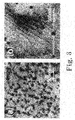
- FIG. 2 shows atomic force microscopy (AFM) images showing a comparison of a layer grown with and without the nanosculpting process and provides an evaluation of the effectiveness of the nanosculpted layer in a single-stage dislocation filter.
- AFM atomic force microscopy
- FIG. 3 shows AFM images of (a) the starting MOCVD GaN template and (b) the surface after 200 nm of MBE growth on top of a single stage filter structure.
- Image (b) corresponds to growth of regions A, B, and C in FIG. 1 .
- the dislocation density was reduced from 2 ⁇ 10 10 to 2 ⁇ 10 8 defects cm ⁇ 2 .
- the dislocation density was reduced further to 2 ⁇ 10 7 defects cm ⁇ 2 .
- the present invention provides methods of growing Group-III nitride thin-film structures having reduced dislocation density.
- Methods in accordance with the present invention comprise growing a Group-III nitride thin-film material while applying an ion flux and preferably with a stationary (non-rotating substrate).
- the ion flux is preferably applied as an ion beam at a glancing angle of incidence. Growth under these conditions creates a nanoscale surface corrugation having a characteristic features size, such as can be measured as a wavelength or surface roughness.
- the substrate is rotated in an ion flux which cause the surface corrugation to be reduced.
- the feature size of the corrugation is reduced and the surface essentially becomes smoother.
- the result of forming a surface corrugation and then subsequently reducing or removing the surface corrugation is the formation of a nanosculpted region and polished transition region that effectively filter dislocations. Repeating such nanosculpted and polished regions advantageously provide significant reduction in dislocation density in thin-film structures.
- the thin-film structure 10 in accordance with the present invention is shown.
- the structure is described with respect to gallium nitride but any Group-III nitride can be used.
- the thin-film structure 10 comprises a substrate 12 , gallium nitride base layer 14 , first nanosculpted region 16 , first transition region 18 , first gallium nitride layer 20 , second nanosculpted region 22 , second transition region 24 , and second gallium nitride layer 26 .
- the substrate 12 comprises any substrate with suitable lattice match to the particular Group-III material being grown.
- suitable substrates include sapphire, silicon, silicon carbide, germanium and zinc oxide.
- the base gallium nitride layer 14 is epitaxially grown by any suitable technique such as molecular beam epitaxy or metal organic chemical vapor deposition and has an initial dislocation density.
- the thickness of layer 14 as shown is about 2.1 microns but any desired thickness can be used depending on the desired crystal properties and thin film structure desired.
- the first nanosculpted region 16 is preferably epitaxially grown by molecular beam epitaxy but any suitable technique can be used.
- a glancing angle ion beam is applied which causes a surface corrugation to form.
- the substrate is stationary or rotated at a low enough rotation rate for the surface corrugation to form.
- the growth is stopped and the substrate is rotated at a sufficient rate in the presence of the ion beam to reduce or substantially remove the surface corrugation.
- the same ion beam can be used as in the step of forming the surface corrugation or different parameters can be used. Rotation in the presence of the ion beam forms the polished transition region 18 .
- First gallium nitride layer 20 is then grown by any desired technique. First gallium nitride 20 accordingly has a reduced dislocation density as compared to the dislocation density of base layer 14 .
- the process is repeated to form second nanosculpted region 22 , second transition region 24 and second gallium nitride layer 18 .
- the process can be repeated as many times as desired, wherein each repetition provides further reduction in the dislocation density. It is believed that dislocation densities below 1 ⁇ 10 6 cm ⁇ 2 can be achieved.
- factors to obtaining dislocation reduction are (1) insertion of nanosculpted layers at low temperature, (2) the choice of the characteristic length scale in the nanosculpted region, (3) the prevention of excessive roughness from forming while the nanosculpted region was prepared, and (4) sufficient surface smoothening in the transition region.
- the use of the glancing angle ion beam not only forms the nanosculpted region but inhibits the formation of Ga droplets at the low temperatures required for the growth.
- the nanoscale features correspond to a surface with a strain modulation.
- the dislocations below this layer are forced to the side or to either coalesce into nanopipes or annihilate.
- the other possibility is that the nanostructure acts as sites to end dislocations, but this would require a defected region to have formed.
- This method could be a very general approach to filtering dislocations, depending on the role of the glide plane of this wurtzite structure.
- Exemplary methods for forming structures such as shown in FIG. 1 in accordance with the present invention are described below.
- MBE molecular beam epitaxy
- Gallium was provided by a conventional effusion cell.
- the nitrogen source was an SVTA (of Eden Prairie Minn.) RF plasma source operated at 325 W of forward RF power and a N 2 pressure of 8 ⁇ 10 ⁇ 6 Torr.
- a broad beam, Kaufman ion source from Ion Tech Inc. was mounted at a glancing angle of 4 degrees to provide an ion flux over the entire sample surface with an angular spread of about 3 degrees. Any glancing angle and spread that create the desired surface corrugation and smoothing can be used.
- Space charge neutral ion beams were obtained by use of a tungsten filament neutralizer.
- the working pressure for the plasma in the MBE growth chamber was in the range of 1.5 to 5.5 ⁇ 10 ⁇ 5 Torr.
- the argon ion beam had a flux density of about 1.6 ⁇ 10 13 ions-cm ⁇ 2 -s ⁇ 1 at 60 to 500 eV.
- Other ion species and flux densities are contemplated and can be determined empirically by one of skill in the art.
- the sample surfaces were characterized in situ by reflection high energy electron diffraction (RHEED) at all stages of the growth and other suitable techniques can be used.
- RHEED reflection high energy electron diffraction
- An Al-coated phosphor screen was used to block the light inside the growth chamber, which allowed recording the RHEED pattern during operation of the Kaufman ion source.
- the surface morphology measurements were conducted ex situ using tapping mode atomic force microscope (AFM) operated in air.
- AFM tapping mode atomic force microscope
- MOCVD GaN samples were grown on basal plane sapphire substrates by APA Enterprises of Blaine Minn. All surfaces were gallium polar, based on the RHEED pattern. The substrate temperature was measured by a thermocouple pressed against the backside of the sample, and the measured temperature offset to the sample surface was calibrated using desorption mass spectroscopy. Non-contact optical temperature measurement techniques can also be used.
- a GaN MOCVD sample was divided into 1 cm ⁇ 1 cm sections and their morphologies compared after different processing steps. The growth rate was about 0.2 ML/s (monolayers/s), limited by the nitrogen flux. Any desired growth rate can be used. The small ion flux changed the growth rate by less than 10%.
- the starting etch pit densities ranged from 2-6 ⁇ 10 10 cm ⁇ 2 .
- the density of threading dislocations in the films is represented by the pit density at the surface.
- an ammonia anneal at 3 ⁇ 10 ⁇ 7 Torr, or equivalently an RF plasma with nitrogen is used as a vacuum etch to reveal the dislocation pits. This compared to the density revealed by molten KOH etching to within 25%.
- the KOH used in this work is 99.99% pure molten base at temperature of 200 degrees C.
- the etching rate, 40 nm/min was measured by a step profiler. During the etching, samples were immersed in molten KOH in a humidity controlled clean hood for about 60 s, corresponding to the removal of about 155 ML of GaN. Residual gallium droplets, if any, were also removed by etching. This amount of etching was insufficient to cause the etch pits to grow enough to coalesce.
- FIG. 1 A schematic of the dislocation filter structure grown is shown in FIG. 1 for the case of a double stage filter on MOCVD GaN grown on a basal plane sapphire substrate and described in more detail above. Any number of filter stages can be used.
- Each filter stage contained three main layers: a nanosculpted layer, A, in which the nanoscale features were created, a transition region, B, obtained by ion polishing of the layer A, and a growth layer with a reduced dislocation density.
- the nanosculpted layer, A was prepared by MBE growth while simultaneously applying a glancing-angle, Ar ion flux.
- the layer thickness ranged between 20 and 100 nm and any desired thickness can be used.
- the Ar ion energy was between 60-500 eV at an ion flux from 1.6 ⁇ 150 ⁇ 10 13 ions-cm ⁇ 2 -s ⁇ 1 .
- the feature size of the corrugation was found to increase from 100 to 800 nm depending on ion energy and etch time and so, to some extent, could be matched to the dislocation density.
- the nanosculpting process was monitored with RHEED to maintain a relatively flat surface. If the surface became too rough, as indicated by the appearance of 3D, transmission features, a smooth surface could not be recovered later.
- the nanosculpted layer comprises a greater concentration of gallium as compared to the gallium nitride grown at higher temperatures and can be measured and used to identify the nanosculpted layer by techniques know to those in the art. Also, it is believed that a bending of dislocations or ending of dislocation can be seen in this region by transmission electron microscopy.
- FIG. 2 A comparison of a layer grown with and without the nanosculpting process is shown in FIG. 2 which provides an evaluation of the effectiveness of the nanosculpted layer in a single-stage dislocation filter.
- the nanosculpted region A was formed with the Ar ion beam.
- the sample was rotated during ion etching and growth so that the rippled nanostructure was not formed.
- This AFM shows the nanosculpted region A without the polished, transition region B in which growth is interrupted. The height range was set to 20 nm.
- FIG. 1 These AFM images show the surface morphology of an exemplary film structure described in FIG. 1 , stopping the process after the growth of the nanosculpted layer, A.
- an Ar flux of 1.6 ⁇ 10 13 ions-cm ⁇ 2 -s ⁇ 1 for 15 min was used with an ion energy of 100 eV.
- Any ion species, incidence angle, spread angle, and source, can be used that provides a surface corrugation and/or polishing in accordance with the present invention.
- FIG. 2( a ) there was no sample rotation during ion assisted growth.
- FIG. 2( a ) there was no sample rotation during ion assisted growth.
- the polished, transition region, B is believed critical for reduction of the dislocation density.
- MBE growth was stopped.
- the same ion beam flux was used as during growth of the nanosculpted layer (other ion beam parameters can be used, however), but now the sample was rotated at a rate of 1.2 rpm.
- the substrate temperature was held at 500 degrees C.
- the sample rotation began prior to interruption of the growth flux.
- Ions then etched the surface for several seconds, not enough to affect smooth regions, until the RHEED patterns reverted to sharp streaky patterns.
- ammonia was used to consume the surface gallium, at 700 degrees C., before restarting the growth of the main layer.
- the polished region comprises a greater concentration of gallium as compared to the gallium nitride grown at higher temperatures and can be measured and used to identify the polished region by techniques know to those in the art. Also, it is believed that a bending of dislocations or ending of dislocation can be seen in this region by transmission electron microscopy.
- FIG. 3 shows AFM images of (a) the starting MOCVD GaN template and (b) the surface after 200 nm of MBE growth on top of a single stage filter structure. Image (b) corresponds to growth of regions A, B, and C in FIG. 1 .
- the dislocation density was reduced from 2 ⁇ 10 10 to 2 ⁇ 10 8 cm ⁇ 2 . In a two stage filter the dislocation density was reduced further to 2 ⁇ 10 7 cm ⁇ 2 .
- the dislocation density was reduced to 2 ⁇ 10 7 cm ⁇ 2 .
- additional stages it is believed that the dislocation density can be reduced to below 1 ⁇ 10 6 cm ⁇ 2 .
Abstract
Description
- 1. P. Gibart, Reports on Progress in Physics 67, 667
- 2. H. Amano, M. Iwaya, T. Kashima, M. Katsuragawa, I. Akasaki, J. Han, S. Hearne, J. A. Floro, E. Chason, and J. Figiel, Jpn. J. Appl. Phys. 37, L1540
- 3. X. L. Fang, Y. Q. Wang, H. Meidia, and S. Mahajan, Appl. Phys. Lett. 84, 484
- 4. K. J. Lee, E. H. Shin, and K. Y. Lim, Appl. Phys. Lett. 85, 1502
- 5. S. Tanaka, M. Takeuchi, and Y. Aoyagi, Jpn. J. Appl. Phys, pt 2 39, 831
- 6. D. Huang, M. Reshchikov, F. Yun, T. King, A. Baski, and H. Morkoc, Appl. Phys. Lett. 80, 216
- 7. M. Sumiya, Y. Kurumasa, K. Ohtsuka, K. Kuwahara, Y. Takano, and S. Fuke, J. Cryst. Growth 237-239, 1060
- 8. K. Jeganathan, M. Shimizu, and H. Okumura, Appl. Phys. Lett. 86, 191908
- 9. S. Nitta, T. Kashima, R. Nakamura, M. Iwaya, H. Amano, and I. Akasaki, Surf. Review and Lett. 7, 561
- 10. C. Ashby, C. Willan, J. Han, N. Missert, P. Provencio, D. Follstaedt, G. Peake, and L. Griego, Appl. Phys. Lett. 77, 3233
- 11. B. Cui, P. I. Cohen, and A. M. Dabiran, J. Appl. Phys. 97, 104313
- 12. R. L. Headrick, S. Kycia, A. R. Woll, J. D. Brock, and M. V. Ramana Murty, Phys. Rev. B 58, 4818
- 13. P. M. DeLuca, K. C. Ruthe, and S. A. Barnett, Phys. Rev. Lett. 86, 260
- 14. R. M. Bradley and J. M. E. Harper, J. Vac. Sci. Technol. A 6, 2390
- 15. R. M. Bradley, Phys. Rev. E 54, 6149
- 16. B. Cui, P. I. Cohen, and A. M. Dabiran, J. Appl. Phys. 98, 083504
- 17. B. Cui and P. I. Cohen, to be submitted to J. Appl. Phys.
- 18. H. Hansen, C. Polop, T. Michely, A. Friedrich, and H. M. Urbassek, Phys. Rev. Lett. 92, 246106
- 19. V. Narayanan, K. Lorenz, and S. Mahajan, Phil. Mag. A 82, 885
- 20. R. Held, G. Nowak, B. E. Ishaug, S. M. Seutter, A. Parkhomovsky, A. M. Dabiran, P. I. Cohen, I. Grzegory, and S. Porowski, J. Appl. Phys., 85, 7697
- 21. R. Held, D. E. Crawford, A. M. Johnston, A. M. Dabiran, and P. I. Cohen, J. Electron. Mater. 26, 272
- 22. H. Morkoc, M. A. Reshchikov, K. M. Jones, F. Yun, P. Visconti, M. I. Nathan, and R. J. Molnar, Mat. Res. Soc. Symp. 639, G11.2.1
- 23. A. Parkhomovsky, A. M. Dabiran, B. Benjaminsson, and P. I. Cohen, Appl. Phys. Lett. 78, 2315
- 24. P. Visconti, D. Huang, F. Yun, M. Reshchikov, T. King, R. Cingolani, J. Jasinski, Z. Liliental-Weber, and H. Morkoc, Phys. Stat. Sol. A 190, 5
- 25. A. Ichimiya and P. 1. Cohen (Cambridge University Press, 2004).
- 26. J. Li, D. Stein, C. McMullan, D. Branton, M. Aziz, and J. Golovchenko, Nature 412, 166
Claims (14)
Priority Applications (1)
| Application Number | Priority Date | Filing Date | Title |
|---|---|---|---|
| US11/810,122 US7879697B2 (en) | 2006-06-05 | 2007-06-04 | Growth of low dislocation density Group-III nitrides and related thin-film structures |
Applications Claiming Priority (2)
| Application Number | Priority Date | Filing Date | Title |
|---|---|---|---|
| US81113306P | 2006-06-05 | 2006-06-05 | |
| US11/810,122 US7879697B2 (en) | 2006-06-05 | 2007-06-04 | Growth of low dislocation density Group-III nitrides and related thin-film structures |
Publications (2)
| Publication Number | Publication Date |
|---|---|
| US20100090311A1 US20100090311A1 (en) | 2010-04-15 |
| US7879697B2 true US7879697B2 (en) | 2011-02-01 |
Family
ID=38832304
Family Applications (1)
| Application Number | Title | Priority Date | Filing Date |
|---|---|---|---|
| US11/810,122 Expired - Fee Related US7879697B2 (en) | 2006-06-05 | 2007-06-04 | Growth of low dislocation density Group-III nitrides and related thin-film structures |
Country Status (3)
| Country | Link |
|---|---|
| US (1) | US7879697B2 (en) |
| TW (1) | TWI356508B (en) |
| WO (1) | WO2007145873A2 (en) |
Cited By (1)
| Publication number | Priority date | Publication date | Assignee | Title |
|---|---|---|---|---|
| US10170303B2 (en) | 2016-05-26 | 2019-01-01 | Robbie J. Jorgenson | Group IIIA nitride growth system and method |
Families Citing this family (1)
| Publication number | Priority date | Publication date | Assignee | Title |
|---|---|---|---|---|
| CN102610717B (en) * | 2011-01-20 | 2015-02-25 | 赛恩倍吉科技顾问(深圳)有限公司 | Semiconductor lighting chip and manufacturing method thereof |
Citations (33)
| Publication number | Priority date | Publication date | Assignee | Title |
|---|---|---|---|---|
| US4916088A (en) | 1988-04-29 | 1990-04-10 | Sri International | Method of making a low dislocation density semiconductor device |
| US5063166A (en) | 1988-04-29 | 1991-11-05 | Sri International | Method of forming a low dislocation density semiconductor device |
| EP0482648A1 (en) | 1990-10-25 | 1992-04-29 | Nichia Kagaku Kogyo K.K. | Method of vapor-growing semiconductor crystal and apparatus for vapor-growing the same |
| US5120393A (en) | 1990-01-12 | 1992-06-09 | Matsushita Electric Industrial Co., Ltd. | Method for molecular-beam epitaxial growth |
| US6251835B1 (en) * | 1997-05-08 | 2001-06-26 | Epion Corporation | Surface planarization of high temperature superconductors |
| US6261931B1 (en) | 1997-06-20 | 2001-07-17 | The Regents Of The University Of California | High quality, semi-insulating gallium nitride and method and system for forming same |
| US20010012678A1 (en) | 1999-12-14 | 2001-08-09 | Satoru Tanaka | Method for the formation of semiconductor layer |
| US20010013313A1 (en) * | 2000-02-10 | 2001-08-16 | Motorola, Inc. | Apparatus for fabricating semiconductor structures and method of forming the structures |
| JP2001288000A (en) | 2000-04-04 | 2001-10-16 | Hitachi Ltd | Method for producing semiconductor thin film crystal |
| US20020069817A1 (en) | 2000-07-21 | 2002-06-13 | Mishra Umesh Kumar | Method to reduce the dislocation density in group III-nitride films |
| JP2002217116A (en) | 2001-01-18 | 2002-08-02 | Sony Corp | Method for manufacturing crystal film, crystal substrate, and semiconductor device |
| EP1245701A2 (en) | 2001-03-28 | 2002-10-02 | Ngk Insulators, Ltd. | A method of fabricating a Group III nitride film |
| JP2002289538A (en) | 2001-03-27 | 2002-10-04 | Univ Meijo | Method for fabricating semiconductor element and semiconductor element |
| JP2002299249A (en) | 2001-03-29 | 2002-10-11 | Sanyo Electric Co Ltd | Semiconductor substrate, semiconductor element and method for forming semiconductor layer |
| JP2002338396A (en) | 2001-05-14 | 2002-11-27 | Nippon Telegr & Teleph Corp <Ntt> | Nitride semiconductor substrate and method for producing the same |
| US6667184B2 (en) | 2001-09-19 | 2003-12-23 | Sumitomo Electric Industries, Ltd. | Single crystal GaN substrate, method of growing same and method of producing same |
| US20040057482A1 (en) | 2002-09-25 | 2004-03-25 | Cao Group, Inc. | GaN structures having low dislocation density and methods of manufacture |
| JP2004099337A (en) | 2002-09-05 | 2004-04-02 | Ngk Insulators Ltd | Group iii nitride film, epitaxial substrate and multilayer film structure |
| JP2004158850A (en) | 2002-11-04 | 2004-06-03 | Lg Philips Lcd Co Ltd | Forming method for polycrystalline silicon film and manufacturing method for thin-film transistor using same |
| WO2004061909A1 (en) | 2002-12-16 | 2004-07-22 | The Regents Of The University Of California | Growth of reduced dislocation density non-polar gallium nitride by hydride vapor phase epitaxy |
| US6784085B2 (en) | 2000-11-30 | 2004-08-31 | North Carolina State University | MIIIN based materials and methods and apparatus for producing same |
| WO2004112112A1 (en) | 2003-06-10 | 2004-12-23 | Sumitomo Electric Industries, Ltd. | Iii nitride crystal and method for producing same |
| JP2004363349A (en) | 2003-06-05 | 2004-12-24 | Shiro Sakai | Nitride system compound semiconductor device and light emitting device |
| US20050103257A1 (en) | 2003-11-13 | 2005-05-19 | Xueping Xu | Large area, uniformly low dislocation density GaN substrate and process for making the same |
| US20050142391A1 (en) | 2001-07-06 | 2005-06-30 | Technologies And Devices International, Inc. | Method and apparatus for fabricating crack-free Group III nitride semiconductor materials |
| US20050183658A1 (en) | 2001-10-09 | 2005-08-25 | Sumitomo Electric Industries, Ltd. | AlxInyGa1-x-yN mixture crystal substrate, method of growing AlxInyGa1-x-yN mixture crystal substrate and method of producing AlxInyGa1-x-yN mixture crystal substrate |
| US6943128B2 (en) | 2000-08-24 | 2005-09-13 | Toyoda Gosei Co., Ltd. | Method for reducing semiconductor resistance, device for reducing semiconductor resistance and semiconductor element |
| US7105865B2 (en) | 2001-09-19 | 2006-09-12 | Sumitomo Electric Industries, Ltd. | AlxInyGa1−x−yN mixture crystal substrate |
| US7112830B2 (en) | 2002-11-25 | 2006-09-26 | Apa Enterprises, Inc. | Super lattice modification of overlying transistor |
| US7118813B2 (en) | 2003-11-14 | 2006-10-10 | Cree, Inc. | Vicinal gallium nitride substrate for high quality homoepitaxy |
| US20060278611A1 (en) * | 2003-09-30 | 2006-12-14 | Japan Aviation Electronics Industry Limited | Method and device for flattening surface of solid |
| US7154131B2 (en) | 2003-10-03 | 2006-12-26 | Sumitomo Electric Industries, Ltd. | Nitride semiconductor substrate and method of producing same |
| US20070141814A1 (en) * | 2005-12-21 | 2007-06-21 | Freiberger Compound Materials Gmbh | Process for producing a free-standing iii-n layer, and free-standing iii-n substrate |
-
2007
- 2007-06-04 US US11/810,122 patent/US7879697B2/en not_active Expired - Fee Related
- 2007-06-04 WO PCT/US2007/013095 patent/WO2007145873A2/en active Application Filing
- 2007-06-05 TW TW096120251A patent/TWI356508B/en not_active IP Right Cessation
Patent Citations (36)
| Publication number | Priority date | Publication date | Assignee | Title |
|---|---|---|---|---|
| US4916088A (en) | 1988-04-29 | 1990-04-10 | Sri International | Method of making a low dislocation density semiconductor device |
| US5063166A (en) | 1988-04-29 | 1991-11-05 | Sri International | Method of forming a low dislocation density semiconductor device |
| US5120393A (en) | 1990-01-12 | 1992-06-09 | Matsushita Electric Industrial Co., Ltd. | Method for molecular-beam epitaxial growth |
| EP0482648A1 (en) | 1990-10-25 | 1992-04-29 | Nichia Kagaku Kogyo K.K. | Method of vapor-growing semiconductor crystal and apparatus for vapor-growing the same |
| US6251835B1 (en) * | 1997-05-08 | 2001-06-26 | Epion Corporation | Surface planarization of high temperature superconductors |
| US6261931B1 (en) | 1997-06-20 | 2001-07-17 | The Regents Of The University Of California | High quality, semi-insulating gallium nitride and method and system for forming same |
| US20010012678A1 (en) | 1999-12-14 | 2001-08-09 | Satoru Tanaka | Method for the formation of semiconductor layer |
| US20010013313A1 (en) * | 2000-02-10 | 2001-08-16 | Motorola, Inc. | Apparatus for fabricating semiconductor structures and method of forming the structures |
| JP2001288000A (en) | 2000-04-04 | 2001-10-16 | Hitachi Ltd | Method for producing semiconductor thin film crystal |
| US6610144B2 (en) | 2000-07-21 | 2003-08-26 | The Regents Of The University Of California | Method to reduce the dislocation density in group III-nitride films |
| US20020069817A1 (en) | 2000-07-21 | 2002-06-13 | Mishra Umesh Kumar | Method to reduce the dislocation density in group III-nitride films |
| US6943128B2 (en) | 2000-08-24 | 2005-09-13 | Toyoda Gosei Co., Ltd. | Method for reducing semiconductor resistance, device for reducing semiconductor resistance and semiconductor element |
| US6784085B2 (en) | 2000-11-30 | 2004-08-31 | North Carolina State University | MIIIN based materials and methods and apparatus for producing same |
| JP2002217116A (en) | 2001-01-18 | 2002-08-02 | Sony Corp | Method for manufacturing crystal film, crystal substrate, and semiconductor device |
| JP2002289538A (en) | 2001-03-27 | 2002-10-04 | Univ Meijo | Method for fabricating semiconductor element and semiconductor element |
| EP1245701A2 (en) | 2001-03-28 | 2002-10-02 | Ngk Insulators, Ltd. | A method of fabricating a Group III nitride film |
| JP2002299249A (en) | 2001-03-29 | 2002-10-11 | Sanyo Electric Co Ltd | Semiconductor substrate, semiconductor element and method for forming semiconductor layer |
| JP2002338396A (en) | 2001-05-14 | 2002-11-27 | Nippon Telegr & Teleph Corp <Ntt> | Nitride semiconductor substrate and method for producing the same |
| US20050142391A1 (en) | 2001-07-06 | 2005-06-30 | Technologies And Devices International, Inc. | Method and apparatus for fabricating crack-free Group III nitride semiconductor materials |
| US6667184B2 (en) | 2001-09-19 | 2003-12-23 | Sumitomo Electric Industries, Ltd. | Single crystal GaN substrate, method of growing same and method of producing same |
| US20060273343A1 (en) | 2001-09-19 | 2006-12-07 | Sumitomo Electric Industries, Ltd. | A1xInyGa1-x-yN mixture crystal substrate, method of growing same and method of producing same |
| US7105865B2 (en) | 2001-09-19 | 2006-09-12 | Sumitomo Electric Industries, Ltd. | AlxInyGa1−x−yN mixture crystal substrate |
| US20050183658A1 (en) | 2001-10-09 | 2005-08-25 | Sumitomo Electric Industries, Ltd. | AlxInyGa1-x-yN mixture crystal substrate, method of growing AlxInyGa1-x-yN mixture crystal substrate and method of producing AlxInyGa1-x-yN mixture crystal substrate |
| JP2004099337A (en) | 2002-09-05 | 2004-04-02 | Ngk Insulators Ltd | Group iii nitride film, epitaxial substrate and multilayer film structure |
| US20040057482A1 (en) | 2002-09-25 | 2004-03-25 | Cao Group, Inc. | GaN structures having low dislocation density and methods of manufacture |
| JP2004158850A (en) | 2002-11-04 | 2004-06-03 | Lg Philips Lcd Co Ltd | Forming method for polycrystalline silicon film and manufacturing method for thin-film transistor using same |
| US6849525B2 (en) | 2002-11-04 | 2005-02-01 | Lg.Philips Lcd Co., Ltd. | Methods for forming polycrystalline silicon layer and fabricating polycrystalline silicon thin film transistor |
| US7112830B2 (en) | 2002-11-25 | 2006-09-26 | Apa Enterprises, Inc. | Super lattice modification of overlying transistor |
| WO2004061909A1 (en) | 2002-12-16 | 2004-07-22 | The Regents Of The University Of California | Growth of reduced dislocation density non-polar gallium nitride by hydride vapor phase epitaxy |
| JP2004363349A (en) | 2003-06-05 | 2004-12-24 | Shiro Sakai | Nitride system compound semiconductor device and light emitting device |
| WO2004112112A1 (en) | 2003-06-10 | 2004-12-23 | Sumitomo Electric Industries, Ltd. | Iii nitride crystal and method for producing same |
| US20060278611A1 (en) * | 2003-09-30 | 2006-12-14 | Japan Aviation Electronics Industry Limited | Method and device for flattening surface of solid |
| US7154131B2 (en) | 2003-10-03 | 2006-12-26 | Sumitomo Electric Industries, Ltd. | Nitride semiconductor substrate and method of producing same |
| US20050103257A1 (en) | 2003-11-13 | 2005-05-19 | Xueping Xu | Large area, uniformly low dislocation density GaN substrate and process for making the same |
| US7118813B2 (en) | 2003-11-14 | 2006-10-10 | Cree, Inc. | Vicinal gallium nitride substrate for high quality homoepitaxy |
| US20070141814A1 (en) * | 2005-12-21 | 2007-06-21 | Freiberger Compound Materials Gmbh | Process for producing a free-standing iii-n layer, and free-standing iii-n substrate |
Non-Patent Citations (27)
Cited By (2)
| Publication number | Priority date | Publication date | Assignee | Title |
|---|---|---|---|---|
| US10170303B2 (en) | 2016-05-26 | 2019-01-01 | Robbie J. Jorgenson | Group IIIA nitride growth system and method |
| US11651959B2 (en) | 2016-05-26 | 2023-05-16 | Robbie J. Jorgenson | Method and system for group IIIA nitride growth |
Also Published As
| Publication number | Publication date |
|---|---|
| TW200816521A (en) | 2008-04-01 |
| US20100090311A1 (en) | 2010-04-15 |
| WO2007145873A3 (en) | 2008-02-21 |
| WO2007145873A2 (en) | 2007-12-21 |
| TWI356508B (en) | 2012-01-11 |
Similar Documents
| Publication | Publication Date | Title |
|---|---|---|
| Oliver et al. | Growth modes in heteroepitaxy of InGaN on GaN | |
| Ng et al. | Growth mode and strain evolution during InN growth on GaN (0001) by molecular-beam epitaxy | |
| CA2712148C (en) | Method for producing a laminated body having a1-based group-iii nitride single crystal layer, laminated body produced by the method, method for producing a1-based group-iii nitride single crystal substrate employing the laminated body, and aluminum nitride single crystal substrate | |
| KR102192130B1 (en) | Iii-n single crystals | |
| US8148246B2 (en) | Method for separating semiconductor layer from substrate | |
| JP2010251776A (en) | Method for manufacturing gallium nitride film separated from substrate by epitaxy | |
| JP2011119761A (en) | Iii-v group nitride semiconductor substrate | |
| Chen et al. | Two-dimensional growth of ZnO films on sapphire (0 0 0 1) with buffer layers | |
| JP2007204359A (en) | Process for producing free-standing iii-n layer, and free-standing iii-n substrate | |
| JP2008004962A (en) | Method for producing iii-v/ii-vi semiconductor interface | |
| JP2004111848A (en) | Sapphire substrate, epitaxial substrate using it, and its manufacturing method | |
| JP2008074671A (en) | Manufacturing method of free-standing nitride substrate | |
| Hu et al. | Growth of self-assembled GaN quantum dots via the vapor–liquid–solid mechanism | |
| KR101458629B1 (en) | MANUFACTURE METHOD FOR ZnO-CONTAINING COMPOUND SEMICONDUCTOR LAYER | |
| Wang et al. | Effect of ZnO buffer layer on the quality of GaN films deposited by pulsed laser ablation | |
| Chen et al. | Plasma-assisted molecular beam epitaxy for ZnO based II–VI semiconductor oxides and their heterostructures | |
| FR2853141A1 (en) | Semiconductor device comprises monocrystalline diboride substrate, semiconductor stopper layer and nitride semiconductor layer, for light emitting and receiving and other electronic devices | |
| US7879697B2 (en) | Growth of low dislocation density Group-III nitrides and related thin-film structures | |
| JP2000315653A (en) | Formation method of quantum dot of nitride semiconductor in droplet epitaxy | |
| Rogers et al. | ZnO thin film templates for GaN-based devices | |
| Chen et al. | Plasma-assisted molecular beam epitaxy of ZnO thin films on sapphire substrates with an MgO buffer | |
| Wuu et al. | Influences of temperature ramping rate on GaN buffer layers and subsequent GaN overlayers grown by metalorganic chemical vapor deposition | |
| JP3504851B2 (en) | Method for manufacturing compound semiconductor film | |
| FR2921200A1 (en) | EPITAXIC MONOLITHIC SEMICONDUCTOR HETEROSTRUCTURES AND PROCESS FOR THEIR MANUFACTURE | |
| JP5024765B2 (en) | Method for cleaning oxide substrate and method for manufacturing oxide semiconductor thin film |
Legal Events
| Date | Code | Title | Description |
|---|---|---|---|
| AS | Assignment |
Owner name: UNITED STATES AIR FORCE,VIRGINIA Free format text: CONFIRMATORY LICENSE;ASSIGNOR:UNIVERSITY OF MINNESOTA, REGENTS OF THE;REEL/FRAME:021991/0662 Effective date: 20070627 Owner name: UNITED STATES AIR FORCE, VIRGINIA Free format text: CONFIRMATORY LICENSE;ASSIGNOR:UNIVERSITY OF MINNESOTA, REGENTS OF THE;REEL/FRAME:021991/0662 Effective date: 20070627 |
|
| AS | Assignment |
Owner name: NATIONAL SCIENCE FOUNDATION,VIRGINIA Free format text: CONFIRMATORY LICENSE;ASSIGNOR:UNIVERSITY OF MINNESOTA;REEL/FRAME:024426/0150 Effective date: 20070627 Owner name: NATIONAL SCIENCE FOUNDATION, VIRGINIA Free format text: CONFIRMATORY LICENSE;ASSIGNOR:UNIVERSITY OF MINNESOTA;REEL/FRAME:024426/0150 Effective date: 20070627 |
|
| STCF | Information on status: patent grant |
Free format text: PATENTED CASE |
|
| FPAY | Fee payment |
Year of fee payment: 4 |
|
| MAFP | Maintenance fee payment |
Free format text: PAYMENT OF MAINTENANCE FEE, 8TH YR, SMALL ENTITY (ORIGINAL EVENT CODE: M2552) Year of fee payment: 8 |
|
| FEPP | Fee payment procedure |
Free format text: MAINTENANCE FEE REMINDER MAILED (ORIGINAL EVENT CODE: REM.); ENTITY STATUS OF PATENT OWNER: SMALL ENTITY |
|
| LAPS | Lapse for failure to pay maintenance fees |
Free format text: PATENT EXPIRED FOR FAILURE TO PAY MAINTENANCE FEES (ORIGINAL EVENT CODE: EXP.); ENTITY STATUS OF PATENT OWNER: SMALL ENTITY |
|
| STCH | Information on status: patent discontinuation |
Free format text: PATENT EXPIRED DUE TO NONPAYMENT OF MAINTENANCE FEES UNDER 37 CFR 1.362 |
|
| FP | Lapsed due to failure to pay maintenance fee |
Effective date: 20230201 |