US8883047B2 - Thermoelectric skutterudite compositions and methods for producing the same - Google Patents
Thermoelectric skutterudite compositions and methods for producing the same Download PDFInfo
- Publication number
- US8883047B2 US8883047B2 US12/990,268 US99026809A US8883047B2 US 8883047 B2 US8883047 B2 US 8883047B2 US 99026809 A US99026809 A US 99026809A US 8883047 B2 US8883047 B2 US 8883047B2
- Authority
- US
- United States
- Prior art keywords
- skutterudite
- materials
- temperature
- samples
- thermoelectric
- Prior art date
- Legal status (The legal status is an assumption and is not a legal conclusion. Google has not performed a legal analysis and makes no representation as to the accuracy of the status listed.)
- Expired - Fee Related, expires
Links
Images


Classifications
-
- H01L35/18—
-
- B22F1/0018—
-
- B—PERFORMING OPERATIONS; TRANSPORTING
- B22—CASTING; POWDER METALLURGY
- B22F—WORKING METALLIC POWDER; MANUFACTURE OF ARTICLES FROM METALLIC POWDER; MAKING METALLIC POWDER; APPARATUS OR DEVICES SPECIALLY ADAPTED FOR METALLIC POWDER
- B22F9/00—Making metallic powder or suspensions thereof
- B22F9/02—Making metallic powder or suspensions thereof using physical processes
- B22F9/04—Making metallic powder or suspensions thereof using physical processes starting from solid material, e.g. by crushing, grinding or milling
-
- B—PERFORMING OPERATIONS; TRANSPORTING
- B22—CASTING; POWDER METALLURGY
- B22F—WORKING METALLIC POWDER; MANUFACTURE OF ARTICLES FROM METALLIC POWDER; MAKING METALLIC POWDER; APPARATUS OR DEVICES SPECIALLY ADAPTED FOR METALLIC POWDER
- B22F9/00—Making metallic powder or suspensions thereof
- B22F9/02—Making metallic powder or suspensions thereof using physical processes
- B22F9/14—Making metallic powder or suspensions thereof using physical processes using electric discharge
-
- B—PERFORMING OPERATIONS; TRANSPORTING
- B82—NANOTECHNOLOGY
- B82Y—SPECIFIC USES OR APPLICATIONS OF NANOSTRUCTURES; MEASUREMENT OR ANALYSIS OF NANOSTRUCTURES; MANUFACTURE OR TREATMENT OF NANOSTRUCTURES
- B82Y30/00—Nanotechnology for materials or surface science, e.g. nanocomposites
-
- C—CHEMISTRY; METALLURGY
- C01—INORGANIC CHEMISTRY
- C01G—COMPOUNDS CONTAINING METALS NOT COVERED BY SUBCLASSES C01D OR C01F
- C01G49/00—Compounds of iron
- C01G49/009—Compounds containing, besides iron, two or more other elements, with the exception of oxygen or hydrogen
-
- C—CHEMISTRY; METALLURGY
- C01—INORGANIC CHEMISTRY
- C01G—COMPOUNDS CONTAINING METALS NOT COVERED BY SUBCLASSES C01D OR C01F
- C01G51/00—Compounds of cobalt
- C01G51/006—Compounds containing, besides cobalt, two or more other elements, with the exception of oxygen or hydrogen
-
- C—CHEMISTRY; METALLURGY
- C01—INORGANIC CHEMISTRY
- C01G—COMPOUNDS CONTAINING METALS NOT COVERED BY SUBCLASSES C01D OR C01F
- C01G53/00—Compounds of nickel
- C01G53/006—Compounds containing, besides nickel, two or more other elements, with the exception of oxygen or hydrogen
-
- C—CHEMISTRY; METALLURGY
- C22—METALLURGY; FERROUS OR NON-FERROUS ALLOYS; TREATMENT OF ALLOYS OR NON-FERROUS METALS
- C22C—ALLOYS
- C22C1/00—Making non-ferrous alloys
- C22C1/04—Making non-ferrous alloys by powder metallurgy
- C22C1/0433—Nickel- or cobalt-based alloys
-
- C—CHEMISTRY; METALLURGY
- C22—METALLURGY; FERROUS OR NON-FERROUS ALLOYS; TREATMENT OF ALLOYS OR NON-FERROUS METALS
- C22C—ALLOYS
- C22C1/00—Making non-ferrous alloys
- C22C1/04—Making non-ferrous alloys by powder metallurgy
- C22C1/0466—Alloys based on noble metals
-
- H01L35/26—
-
- H—ELECTRICITY
- H10—SEMICONDUCTOR DEVICES; ELECTRIC SOLID-STATE DEVICES NOT OTHERWISE PROVIDED FOR
- H10N—ELECTRIC SOLID-STATE DEVICES NOT OTHERWISE PROVIDED FOR
- H10N10/00—Thermoelectric devices comprising a junction of dissimilar materials, i.e. devices exhibiting Seebeck or Peltier effects
- H10N10/80—Constructional details
- H10N10/85—Thermoelectric active materials
- H10N10/851—Thermoelectric active materials comprising inorganic compositions
- H10N10/853—Thermoelectric active materials comprising inorganic compositions comprising arsenic, antimony or bismuth
-
- H—ELECTRICITY
- H10—SEMICONDUCTOR DEVICES; ELECTRIC SOLID-STATE DEVICES NOT OTHERWISE PROVIDED FOR
- H10N—ELECTRIC SOLID-STATE DEVICES NOT OTHERWISE PROVIDED FOR
- H10N10/00—Thermoelectric devices comprising a junction of dissimilar materials, i.e. devices exhibiting Seebeck or Peltier effects
- H10N10/80—Constructional details
- H10N10/85—Thermoelectric active materials
- H10N10/857—Thermoelectric active materials comprising compositions changing continuously or discontinuously inside the material
-
- B—PERFORMING OPERATIONS; TRANSPORTING
- B22—CASTING; POWDER METALLURGY
- B22F—WORKING METALLIC POWDER; MANUFACTURE OF ARTICLES FROM METALLIC POWDER; MAKING METALLIC POWDER; APPARATUS OR DEVICES SPECIALLY ADAPTED FOR METALLIC POWDER
- B22F9/00—Making metallic powder or suspensions thereof
- B22F9/02—Making metallic powder or suspensions thereof using physical processes
- B22F9/04—Making metallic powder or suspensions thereof using physical processes starting from solid material, e.g. by crushing, grinding or milling
- B22F2009/043—Making metallic powder or suspensions thereof using physical processes starting from solid material, e.g. by crushing, grinding or milling by ball milling
-
- B—PERFORMING OPERATIONS; TRANSPORTING
- B22—CASTING; POWDER METALLURGY
- B22F—WORKING METALLIC POWDER; MANUFACTURE OF ARTICLES FROM METALLIC POWDER; MAKING METALLIC POWDER; APPARATUS OR DEVICES SPECIALLY ADAPTED FOR METALLIC POWDER
- B22F2203/00—Controlling
- B22F2203/11—Controlling temperature, temperature profile
-
- B—PERFORMING OPERATIONS; TRANSPORTING
- B22—CASTING; POWDER METALLURGY
- B22F—WORKING METALLIC POWDER; MANUFACTURE OF ARTICLES FROM METALLIC POWDER; MAKING METALLIC POWDER; APPARATUS OR DEVICES SPECIALLY ADAPTED FOR METALLIC POWDER
- B22F2998/00—Supplementary information concerning processes or compositions relating to powder metallurgy
- B22F2998/10—Processes characterised by the sequence of their steps
-
- B—PERFORMING OPERATIONS; TRANSPORTING
- B22—CASTING; POWDER METALLURGY
- B22F—WORKING METALLIC POWDER; MANUFACTURE OF ARTICLES FROM METALLIC POWDER; MAKING METALLIC POWDER; APPARATUS OR DEVICES SPECIALLY ADAPTED FOR METALLIC POWDER
- B22F2999/00—Aspects linked to processes or compositions used in powder metallurgy
-
- C—CHEMISTRY; METALLURGY
- C01—INORGANIC CHEMISTRY
- C01P—INDEXING SCHEME RELATING TO STRUCTURAL AND PHYSICAL ASPECTS OF SOLID INORGANIC COMPOUNDS
- C01P2002/00—Crystal-structural characteristics
- C01P2002/50—Solid solutions
- C01P2002/52—Solid solutions containing elements as dopants
-
- C—CHEMISTRY; METALLURGY
- C01—INORGANIC CHEMISTRY
- C01P—INDEXING SCHEME RELATING TO STRUCTURAL AND PHYSICAL ASPECTS OF SOLID INORGANIC COMPOUNDS
- C01P2002/00—Crystal-structural characteristics
- C01P2002/50—Solid solutions
- C01P2002/52—Solid solutions containing elements as dopants
- C01P2002/54—Solid solutions containing elements as dopants one element only
-
- C—CHEMISTRY; METALLURGY
- C01—INORGANIC CHEMISTRY
- C01P—INDEXING SCHEME RELATING TO STRUCTURAL AND PHYSICAL ASPECTS OF SOLID INORGANIC COMPOUNDS
- C01P2002/00—Crystal-structural characteristics
- C01P2002/70—Crystal-structural characteristics defined by measured X-ray, neutron or electron diffraction data
- C01P2002/72—Crystal-structural characteristics defined by measured X-ray, neutron or electron diffraction data by d-values or two theta-values, e.g. as X-ray diagram
-
- C—CHEMISTRY; METALLURGY
- C01—INORGANIC CHEMISTRY
- C01P—INDEXING SCHEME RELATING TO STRUCTURAL AND PHYSICAL ASPECTS OF SOLID INORGANIC COMPOUNDS
- C01P2002/00—Crystal-structural characteristics
- C01P2002/70—Crystal-structural characteristics defined by measured X-ray, neutron or electron diffraction data
- C01P2002/77—Crystal-structural characteristics defined by measured X-ray, neutron or electron diffraction data by unit-cell parameters, atom positions or structure diagrams
-
- C—CHEMISTRY; METALLURGY
- C01—INORGANIC CHEMISTRY
- C01P—INDEXING SCHEME RELATING TO STRUCTURAL AND PHYSICAL ASPECTS OF SOLID INORGANIC COMPOUNDS
- C01P2002/00—Crystal-structural characteristics
- C01P2002/80—Crystal-structural characteristics defined by measured data other than those specified in group C01P2002/70
- C01P2002/88—Crystal-structural characteristics defined by measured data other than those specified in group C01P2002/70 by thermal analysis data, e.g. TGA, DTA, DSC
-
- C—CHEMISTRY; METALLURGY
- C01—INORGANIC CHEMISTRY
- C01P—INDEXING SCHEME RELATING TO STRUCTURAL AND PHYSICAL ASPECTS OF SOLID INORGANIC COMPOUNDS
- C01P2004/00—Particle morphology
- C01P2004/01—Particle morphology depicted by an image
- C01P2004/03—Particle morphology depicted by an image obtained by SEM
-
- C—CHEMISTRY; METALLURGY
- C01—INORGANIC CHEMISTRY
- C01P—INDEXING SCHEME RELATING TO STRUCTURAL AND PHYSICAL ASPECTS OF SOLID INORGANIC COMPOUNDS
- C01P2004/00—Particle morphology
- C01P2004/01—Particle morphology depicted by an image
- C01P2004/04—Particle morphology depicted by an image obtained by TEM, STEM, STM or AFM
-
- C—CHEMISTRY; METALLURGY
- C01—INORGANIC CHEMISTRY
- C01P—INDEXING SCHEME RELATING TO STRUCTURAL AND PHYSICAL ASPECTS OF SOLID INORGANIC COMPOUNDS
- C01P2004/00—Particle morphology
- C01P2004/60—Particles characterised by their size
- C01P2004/64—Nanometer sized, i.e. from 1-100 nanometer
-
- C—CHEMISTRY; METALLURGY
- C01—INORGANIC CHEMISTRY
- C01P—INDEXING SCHEME RELATING TO STRUCTURAL AND PHYSICAL ASPECTS OF SOLID INORGANIC COMPOUNDS
- C01P2006/00—Physical properties of inorganic compounds
- C01P2006/10—Solid density
-
- C—CHEMISTRY; METALLURGY
- C01—INORGANIC CHEMISTRY
- C01P—INDEXING SCHEME RELATING TO STRUCTURAL AND PHYSICAL ASPECTS OF SOLID INORGANIC COMPOUNDS
- C01P2006/00—Physical properties of inorganic compounds
- C01P2006/40—Electric properties
-
- Y—GENERAL TAGGING OF NEW TECHNOLOGICAL DEVELOPMENTS; GENERAL TAGGING OF CROSS-SECTIONAL TECHNOLOGIES SPANNING OVER SEVERAL SECTIONS OF THE IPC; TECHNICAL SUBJECTS COVERED BY FORMER USPC CROSS-REFERENCE ART COLLECTIONS [XRACs] AND DIGESTS
- Y02—TECHNOLOGIES OR APPLICATIONS FOR MITIGATION OR ADAPTATION AGAINST CLIMATE CHANGE
- Y02P—CLIMATE CHANGE MITIGATION TECHNOLOGIES IN THE PRODUCTION OR PROCESSING OF GOODS
- Y02P20/00—Technologies relating to chemical industry
- Y02P20/10—Process efficiency
- Y02P20/129—Energy recovery, e.g. by cogeneration, H2recovery or pressure recovery turbines
-
- Y—GENERAL TAGGING OF NEW TECHNOLOGICAL DEVELOPMENTS; GENERAL TAGGING OF CROSS-SECTIONAL TECHNOLOGIES SPANNING OVER SEVERAL SECTIONS OF THE IPC; TECHNICAL SUBJECTS COVERED BY FORMER USPC CROSS-REFERENCE ART COLLECTIONS [XRACs] AND DIGESTS
- Y10—TECHNICAL SUBJECTS COVERED BY FORMER USPC
- Y10S—TECHNICAL SUBJECTS COVERED BY FORMER USPC CROSS-REFERENCE ART COLLECTIONS [XRACs] AND DIGESTS
- Y10S977/00—Nanotechnology
- Y10S977/70—Nanostructure
- Y10S977/773—Nanoparticle, i.e. structure having three dimensions of 100 nm or less
Definitions
- the present application relates generally to thermoelectric materials and methods for their fabrication, and more particularly, to skutterudite-based thermoelectric materials that exhibit thermoelectric properties.
- Thermoelectric materials can be utilized in a variety of industrial applications including high quality power generation devices and cooling devices. They can also be used in solar conversion and extraction of automotive or industrial waste heat.
- Skutterudites are a potentially attractive class of substances that might be used in producing thermoelectric materials. They typically exhibit outstanding electrical properties, including high electrical charge mobilities and substantial Seebeck coefficients—which can result in high power factors. Unfortunately, they also often exhibit high thermal conductivities, which can limit the overall ZT value that can be achieved by a thermoelectric material.
- thermoelectric materials that exhibit attractive performance properties, including materials that may be related to skutterudites.
- Some embodiments of the present invention are directed to methods of fabricating an enhanced thermoelectric material. Such materials can exhibit good ZT values (e.g., greater than about 0.8), which can occur at one or more selected temperatures (e.g., at a temperature below about 800° C.).
- a plurality of nanoparticles can be generated from one or more starting materials.
- the starting material(s) can be one or more elements, and/or include one or more skutterudite-based starting materials (e.g., two or more skutterudite-based starting materials). When the latter are used, the densified material can exhibit a higher ZT value at least at one temperature relative to at least one of the skutterudite-based starting materials.
- the starting material can optionally include one or more types of filler atoms, which can be used in the skutterudite-based structure.
- Such nanoparticles can be consolidated under pressure and an elevated temperature to form a densified material.
- the densified material can include a plurality of grains, in which each grain can exhibit a skutterudite-based structure.
- the skutterudite-based structure which can be filler-containing, can include a crystal having metal atoms (e.g., having one, two, or more of cobalt, iron, nickel, rhodium, iridium, ruthenium, and osmium) forming a cubic sublattice.
- the grains can exhibit an average size smaller than about 5 microns, and optionally larger than the average size of the nanoparticles from which the densified material was formed.
- generation of nanoparticles can be performed using any number of methodologies.
- generation of nanoparticles can include grinding (e.g., ball milling) at least one starting material to form the nanoparticles.
- the materials can be combined together in any combination and ground, or ground separately to a final disposition for consolidation, or separately ground and then mixed together and ground further to a disposition for consolidation.
- Materials being grinded can also be cooled, which can promote particle formation in some instances.
- the average size of the generated nanoparticles can be smaller than about 50 nm.
- Consolidation of nanoparticles can also be performed using any number of techniques.
- consolidation is performed using a hot press process (e.g., using at least one of direct current induced hot press, unidirectional hot press, plasma pressure compaction, and isostatic hot press).
- the consolidation can occur at a pressure in a range from about 10 MPa to about 900 MPa; and/or using a temperature in a range from about 200° C. to about 800° C.
- the time period to which the nanoparticles are subjected to a pressure and elevated temperature can be between about 1 sec and about 10 hours.
- thermoelectric materials which can include a plurality of compacted crystalline skutterudite-based grains. Such thermoelectric materials can exhibit a ZT value greater than about 0.5, 0.8, or 1.
- the crystalline skutterudite-based grains can include crystallites having metal atoms (e.g., having one, two, or more of cobalt, iron, nickel, rhodium, iridium, ruthenium, and osmium) forming a cubic sublattice.
- Group VA atoms can be included, which can form a plurality of planar rings within the cubic sublattice.
- Filler atoms can also, optionally, be added, where filler atoms can include at least one a rare earth element and a Group IIA element.
- the grains can exhibit an average size of less than about 5000 nm or 1000 nm.
- thermoelectric materials which can include a skutterudite-based structure.
- the structure can include grains each exhibiting a unit cell formed from (i) at least one Group VA element, and (ii) at least one of cobalt, iron, nickel, rhodium, iridium, ruthenium, and osmium.
- the grains can exhibit an average size of less than about 5000 nm or less than about 1000 nm.
- the structure can also include at least one type of filler atom in each unit cell, such as a rare earth element and/or a Group IIA element.
- the at least one filler atom comprises at least one, or at least two, of cerium, neodymium, lanthanum, barium, and ytterbium.
- the structure can be characterized by an enhanced ZT value relative to a bulk material having the skutterudite-based structure.
- the thermoelectric material can exhibit a ZT value greater than about 0.8 or about 1.0; the ZT value can optionally be exhibited at a temperature below about 600° C.
- Thermoelectric materials can include at least one of a n-type material and a p-type material.
- the thermoelectric material is a p-type material.
- the p-type material can include a composition consistent with the formula ReFe 4-y M y Sb ⁇ 12 where Re is at least one of a rare earth element and a Group IIA element (e.g., barium), M is cobalt or nickel or combinations of them with other elements, and y is zero or a positive number no greater than 4.
- the p-type material can include a composition consistent with the formula ReFe 3.5 Co 0.5 Sb ⁇ 12 , where Re is any one of neodymium, cerium, lanthanum, or ytterbium.
- the thermoelectric material is a n-type material.
- the n-type material can include a composition consistent with the formula Re z M y Co 4-y Sb ⁇ 12 where Re is at least one of a rare earth element and a Group IIA element, M is a metal, y is zero or a positive number no greater than 4; and z is a positive number no greater than 1.
- the thermoelectric material can include a composition consistent with a formula: Re z Co ⁇ 4 Sb ⁇ 12 , where z is a number between about 0.2 and about 1, and Re is at least one of cerium, neodymium, lanthanum, barium, and ytterbium.
- thermoelectric material comprises a n-type composition consistent with a formula: Re1 Z1 Re2 Z2 Co ⁇ 4 Sb ⁇ 12 , where Z1 and Z2 are each independently a number between about 0.2 and about 1 with a sum of Z1 and Z2 not greater than about 1, and Re1 and Ret are each independently at least one of cerium, neodymium, lanthanum, barium, and ytterbium.
- the thermoelectric material comprises a composition consistent with a formula: Yb z M y Co 4-y Sb 12 , where z is any number between about 0.2 and about 1, and y is optionally zero.
- thermoelectric materials can include a filler enhanced skutterudite material comprising at least one type of filler, which can be distributed throughout the thermoelectric material.
- the filler enhanced skutterudite material can exhibit a higher fractional amount of the at least one type of filler relative to a maximum achievable equilibrium fractional amount of the at least one type of filler in a bulk form of the filler enhanced skutterudite-based material.
- the materials can include a composition consistent with the formula Yb z Co 4 Sb 12 , where z is any number between about 0.2 and about 1, or between about 0.3 and about 0.5 (e.g., 0.3, 0.4, or 0.5).
- FIG. 1 presents a perspective schematic diagram of a CoSb 3 skutterudite crystal structure, consistent with some embodiments of the present invention
- FIG. 2 a presents a transmission electron micrograph image of a ball milled sample particles before hot pressing, consistent with some embodiments of the invention
- FIG. 2 b presents a transmission electron micrograph at higher magnification that the image of FIG. 2 a within the circular region shown in FIG. 2 a;
- FIG. 3 presents a scanning electron microscopy image of a DC hot pressed sample of Yb 0.35 Co 4 Sb 12 , in accord with some embodiments;
- FIG. 4 presents superimposed graphs of intensity versus angle 2 ⁇ taken from x-ray diffraction scans of five hot-pressed samples each having a stoichiometry corresponding with the formula Yb x Co 4 Sb 12 , where for individual samples x is equal to one of 0.3, 0.35, 0.4, 0.5 and 1.0, consistent with some embodiments;
- FIG. 5 a presents a transmission electron microscopy image of a hot pressed sample having a composition following the formula Yb 0.35 Co 4 Sb 12 , consistent with some embodiments;
- FIG. 5 b presents a transmission electron microscopy image of the hot pressed sample shown in FIG. 5 a at higher magnification
- FIG. 6 presents graphs of carrier concentration and Hall mobility at room temperature for various hot pressed samples having a stoichiometry consistent with the formula Yb x Co 4 Sb 12 , where x ranges from 0.3 to 0.5, consistent with some embodiments;
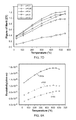
- FIG. 7 a presents graphs of the measured electrical conductivity as a function of temperature for hot pressed samples consistent with the formula Yb x Co 4 Sb 12 , where x is 0.3, 0.35, 0.4, 0.5, and 1, consistent with some embodiments;
- FIG. 7 b presents graphs of the measured Seebeck coefficient as a function of temperature for the hot pressed samples in FIG. 7 a;
- FIG. 7 c presents graphs of the measured thermal conductivity as a function of temperature for the hot pressed samples in FIG. 7 a;
- FIG. 7 d presents graphs of ZT values as a function of temperature for the hot pressed samples in FIG. 7 a;
- FIG. 8 a presents graphs of the measured resistivity as a function of temperature for hot pressed samples having the following stoichiometries: La 0.3 Co 4 Sb 12 , Nd 0.3 Co 4 Sb 12 , and Yb 0.3 Co 4 Sb 12 , consistent with some embodiments;
- FIG. 8 b presents graphs of the measured Seebeck coefficient as a function of temperature for the hot pressed samples in FIG. 8 a;
- FIG. 8 c presents graphs of the calculated power factor as a function of temperature for the hot pressed samples in FIG. 8 a;
- FIG. 8 d presents graphs of the measured thermal conductivity as a function of temperature for the hot pressed samples in FIG. 8 a;
- FIG. 8 e presents graphs of the lattice thermal conductivity as a function of temperature for the hot pressed samples in FIG. 8 a;
- FIG. 8 f presents graphs of ZT values as a function of temperature for the hot pressed samples in FIG. 8 a;
- FIG. 9 a presents graphs of the measured resistivity as a function of temperature for hot pressed samples having the following stoichiometries: La 0.1 Yb 0.3 Co 4 Sb 12 , Ce 0.03 Yb 0.3 Co 4 Sb 12 , Ba 0.1 Yb 0.3 Co 4 Sb 12 , and Yb 0.3 Co 4 Sb 12 , consistent with some embodiments;
- FIG. 9 b presents graphs of the measured Seebeck coefficient as a function of temperature for the hot pressed samples in FIG. 9 a;
- FIG. 9 c presents graphs of the calculated power factor as a function of temperature for the hot pressed samples in FIG. 9 a;
- FIG. 9 d presents graphs of the measured thermal conductivity as a function of temperature for the hot pressed samples in FIG. 9 a;
- FIG. 9 e presents graphs of the lattice thermal conductivity as a function of temperature for the hot pressed samples in FIG. 8 a;
- FIG. 9 f presents graphs of ZT values as a function of temperature for the hot pressed samples in FIG. 8 a;
- FIG. 10 a presents a transmission electron microscopy image of particles having a composition consistent with the formula CeFe 3.5 Co 0.5 Sb 12 after 20 hours of ball milling, consistent with some embodiments;
- FIG. 10 b presents a transmission electron microscopy image of the particles of FIG. 10 a at a higher magnification
- FIG. 11 a presents a scanning electron microscopy image of a DC hot pressed sample of particles made from materials having the stoichiometry CeFe 3.5 Co 0.5 Sb 12 after 20 hours of ball milling, consistent with some embodiments;
- FIG. 11 b presents a transmission electron microscopy image of the sample in FIG. 11 a;
- FIG. 12 a presents graphed data of the measured electrical conductivity as a function of temperature for hot pressed samples of particles having the stoichiometry NdFe 3.5 Co 0.5 Sb 12 , where individual samples used particles ball milled for 15, 20, or 25 hours, consistent with some embodiments;
- FIG. 12 b presents graphed data of measured Seebeck coefficient as a function of temperature for the samples in FIG. 12 a;
- FIG. 12 c presents graphed data of calculated values of the product of the power factor with temperature as a function of temperature for the samples in FIG. 12 a;
- FIG. 12 d presents graphed data of measured thermal conductivity as a function of temperature for the samples in FIG. 12 a;
- FIG. 12 e presents graphed data of ZT values as a function of temperature for the samples in FIG. 12 a;
- FIG. 13 a presents graphed data of the measured electrical conductivity as a function of temperature for hot pressed samples of particles having the stoichiometries NdFe 3.5 Co 0.5 Sb 12 , LaFe 3.5 Co 0.5 Sb 12 , YbFe 3.5 Co 0.5 Sb 12 , and CeFe 3.5 Co 0.5 Sb 12 , where samples used particles ball milled for 20 hours, consistent with some embodiments;
- FIG. 13 b presents graphed data of measured Seebeck coefficient as a function of temperature for the samples in FIG. 13 a;
- FIG. 13 c presents graphed data of calculated values of the product of the power factor with temperature as a function of temperature for the samples in FIG. 13 a;
- FIG. 13 d presents graphed data of measured thermal conductivity as a function of temperature for the samples in FIG. 13 a;
- FIG. 13 e presents graphed data of ZT values as a function of temperature for the samples in FIG. 13 a;
- FIG. 14 a presents graphed data of the measured electrical conductivity as a function of temperature for hot pressed samples of particles having the stoichiometries NdFe 3.5 Co 0.5 Sb 12 and Nd 0.9 Fe 3.5 Co 0.5 Sb 12 , where samples used particles ball milled for 15 s hours, consistent with some embodiments;
- FIG. 14 b presents graphed data of measured Seebeck coefficient as a function of temperature for the samples in FIG. 14 a;
- FIG. 14 c presents graphed data of calculated values of the product of the power factor with temperature as a function of temperature for the samples in FIG. 14 a;
- FIG. 14 d presents graphed data of measured thermal conductivity as a function of temperature for the samples in FIG. 14 a;
- FIG. 14 e presents graphed data of ZT values as a function of temperature for the samples in FIG. 14 a;
- FIG. 15 a presents graphed data of the measured electrical conductivity as a function of temperature for hot pressed samples of particles having the stoichiometries LaFe 3.5 Co 0.5 Sb 12 and La 0.9 Yb 0.1 Fe 3.5 Co 0.5 Sb 12 , where samples used particles ball milled for 15 s hours, consistent with some embodiments;
- FIG. 15 b presents graphed data of measured Seebeck coefficient as a function of temperature for the samples in FIG. 15 a;
- FIG. 15 c presents graphed data of calculated values of the product of the power factor with temperature as a function of temperature for the samples in FIG. 15 a;
- FIG. 15 d presents graphed data of measured thermal conductivity as a function of temperature for the samples in FIG. 15 a ;
- FIG. 15 e presents graphed data of ZT values as a function of temperature for the samples in FIG. 15 a.
- Some embodiments of the present invention are directed to novel compositions and/or methods relating to skutterudite-based thermoelectric materials. Such embodiments can result in improved ZT values such as by modifications that can lower the thermal conductivity of a final thermoelectric material relative to the one or more starting materials from which the final product is made. Improvements in thermoelectric performance can be made in any number of manners described herein, including the use of a final structure with a plurality of grains, and/or incorporation of one or more filler atoms into a unit cell of a skutterudite based crystal, among other modifications which include using more than one of the modifications. These embodiments, among others, are described within the present application.
- Skutterudites are compositions whose principal constituents are typically cobalt or iron, and a Group VA element such as phosphorus, arsenic, antimony or bismuth.
- a Group VA element such as phosphorus, arsenic, antimony or bismuth.
- One example would be a cobalt and antimony containing composition.
- An example of the unit cell structure of a Co 4 Sb 12 skutterudite is shown in FIG. 1 ; in FIG. 1 the unit cell is shifted by one quarter distance along the body diagonal.
- the cobalt atoms are generally arranged in a cubic crystalline structure, forming a cubic sublattice of 8 cubes.
- the atoms of the Group VA element form a secondary crystalline structure within the cobalt cubic unit cell, forming planar rings such as the four-membered rings shown in FIG. 1 .
- Skutterudite-based materials can generally include materials having portions that conform to the structure of one or more skutterudite crystals (e.g., consistent with FIG. 1 ).
- the crystal(s), however, can include modifications.
- the cobalt atoms of FIG. 1 can be replaced, or supplemented, by one or more types of metal atoms, which can include iron, nickel, rhodium, iridium, ruthenium, and osmium.
- Mixed metal atom constituents in a unit cell can include various appropriate combination of metals; nickel/cobalt or cobalt/iron compositions, which are commonly found in natural depositions, are examples of such combinations.
- the Group VA atoms that can be used can include one or more of phosphorous, arsenic, antimony, and bismuth—which can optionally include mixtures thereof.
- one or more types of filler atoms can be included in a skutterudite-based material.
- Types of filler atoms can include any atomic type suitable for inclusion in a skutterudite-based material (e.g., those that can enhance the ZT value of a material).
- the filler atom can include one or more of a rare earth metal and a Group IIA element (e.g., barium).
- Non-limiting examples of such fillers include cerium, neodymium, lanthanum, barium, and ytterbium.
- a filler atom can be located in a void of a crystal unit cell, as shown in FIG. 1 .
- the presence of a filler atom can act as a defect and/or as a void filler, which can potentially depress the thermal conductivity of the material relative to not using a filler atom.
- a filler atom lowers the thermal conductivity of the material because of the dynamics, or rattling, caused by the disorder introduced by a filler atom in the void; loosely bound rattlers can produce local vibrations of lower frequency, and are thus more effective in scattering the lower frequency, heat carrying phonons.
- the amount of a filler atom(s) to be incorporated into a skutterudite-based material can be any to allow the formation of a thermoelectric material with desired properties. Other properties can also be selected to limit the amount of one or more filler atoms. For instance, the amount of a filler can be chosen to be no greater than to allow a single phase material to be formed and/or a single type of crystalline structure to predominate the overall material's structure.
- Re is a filling atom
- M is a transitional metal required by charge compensation
- Ch is a Group VA atom such as antimony or an atom in close proximity to antimony such as tellurium.
- a skutterudite-based material can include one or more portions having a stoichiometry consistent with the following formula: Re1 w Re2 x Fe y Co 4-y Sb ⁇ 12 where w and x each have positive values greater than or equal to zero, optionally their sum is less than about a selected value (e.g., 2 or 1); y has a positive value no greater than 4; Re1 is one type of filler atom (e.g., a rare earth atom); and Re2 is another type of filler atom different than Re1, which can be another rare earth atom or a Group IIA atom (e.g., barium).
- Group VA atoms can be substituted for antimony, and other variations of a skutterudite-based material having multiple types of filler atoms
- Skutterudite-based materials can also include dopants, which can affect the properties of the material.
- the nanoparticles can be compactified with other types of particles such as particles from a source material having a good ZT value (e.g., greater than about 0.5), and/or micron-sized particles (e.g., particles having an average size from about 1 micron to about 10, 50, 100, or 500 microns).
- n-type and p-type skutterudite-based materials can include n-type and p-type skutterudite-based materials. In some instances, these materials can exhibit enhanced thermoelectric figures-of-merit (e.g., greater than 1). Such materials can be advantageously utilized as semiconductor materials, for example as incorporated into a portion of a solar energy device.
- a skutterudite-based material can include a n-type material having a composition consistent with the following general formula: Re z M y Ca 4-y Sb 12 where Re is a rare earth element (e.g., lanthanum, cerium, ytterbium, neodymium, or combinations thereof) or a Group IIA element (e.g., barium, calcium, etc., or combinations thereof); M is a metal (e.g., iron, nickel, or others); y is zero or a positive number no larger than 4; and z is a value greater than zero. In some instances, z is no greater than about 1.
- Re is a rare earth element (e.g., lanthanum, cerium, ytterbium, neodymium, or combinations thereof) or a Group IIA element (e.g., barium, calcium, etc., or combinations thereof)
- M is a metal (e.g., iron, nickel, or others)
- y is
- z has a value greater than about 0.2 or greater than about 0.3. As well, z can also have an upper limit no greater than about 0.5 in some instances. In some embodiments, these potential values of z can be applied when y is substantially zero.
- Re is any one of lanthanum, ytterbium, and neodymium, or Re is ytterbium.
- two or more types of filler atoms can be used, for example: Re1 z1 Re2 z2 M y Co 4-y Sb 12 where z1 and z2 each have positive values such that the sum of z1 and z2 is no greater than about 1 or about 0.5. In some instances, y can be about 2. In some instances using multiple types of filler atoms, one type of atom is ytterbium, and optionally another type is barium.
- a skutterudite material can include a p-type skutterudites can have material having a composition consistent with the following general formula: Re z Fe 4-x M x Sb ⁇ 12 where Re is a rare earth element (e.g., lanthanum, cerium, ytterbium, or neodymium or combinations thereof) or a Group IIA element (e.g., barium, etc.); M is cobalt or nickel or combinations of them with other elements; x is 0 or a positive number no greater than 4; and z is any positive number less than 1 (including zero).
- Re is a rare earth element (e.g., lanthanum, cerium, ytterbium, or neodymium or combinations thereof) or a Group IIA element (e.g., barium, etc.); M is cobalt or nickel or combinations of them with other elements; x is 0 or a positive number no greater than 4; and z is any positive number less than 1
- z is in a range from about 0.05 to about 1, and x is about 0.5; in a particular embodiment, Re is neodymium.
- multiple types of filler atoms can be utilized, for example materials having a stoichiometry consistent with: Re1 z1 Re2 z2 Fe 4-x M x Sb ⁇ 12 where z1 and z2 each have positive values such that the sum of z1 and z2 is no greater than about 1.
- thermoelectric materials can utilize skutterudite-based compositions with stoichiometries as disclosed herein, in some embodiments the materials are formed from a plurality of grains. Such grains can each include at least a portion that has a skutterudite-based structure.
- the skutterudite-based structure can be of any stoichiometry consistent with skutterudite-based materials including those explicitly disclosed herein. Any of these grains can be formed by a plurality of mechanisms including, but not limited to, consolidation of particles (e.g., as described herein) and/or formation by solid-state chemical reaction.
- thermoelectric material can have a variety of characteristics.
- each grain has a crystalline structure.
- the thermoelectric material can comprise a polycrystalline-like structure in which the grains generally lack a preferred orientation (e.g., randomly oriented).
- the grains can also exhibit some type of preferred orientation due to grain shapes, where the general crystalline direction of the grains can either be random or exhibit some preferred direction relative to one another.
- thermoelectric materials consistent with embodiments of the invention can include a variety of sizes of grains.
- the thermoelectric material can have some grains larger than 1 ⁇ m and some grains smaller than 1 ⁇ m.
- the thermoelectric material exhibits an average grain size that is smaller than about a designated size (e.g., 5 microns).
- a designated size e.g., 5 microns.
- Non-limiting examples include about 5000 nm, 3000 nm, 1000 nm, 900 nm, 800 nm, 700 nm, 600 nm, 500 nm, 400 nm, 300 nm, 200 nm, 100 nm, 50 nm, or 10 nm.
- the average grain size can be determined using a variety of methodologies, including methods understood by those skilled in the art.
- TEMs transmission electron micrographs
- the measured size of a grain can be determined using any number of techniques, including ones known to the skilled artisan.
- the largest dimension of the grain can be used from an image (e.g., a scanning electron micrograph image and/or TEM image), or an effective diameter can be calculated based on surface area measurements or the effective-cross sectional area of grains from an image.
- thermoelectric materials having skutterudite-based grains can be the result of variations in combination of the thermal conductivity, the Seebeck coefficient, and the electrical conductivity.
- Thermal conductivity has two contributions: lattice and charge carrier contributions.
- lattice thermal conductivity is fixed for a specific material.
- the lattice part of thermal conductivity can drop due to interface scattering of phonons. Such a decrease in phonon scattering reduces the thermal conductivity to a greater extent relative to the decrease in electrical conductivity, leading to a greater ZT value.
- the Seebeck coefficient can increase because of the carrier filtering effect (usually low energy electrons/holes are scattered thereby increasing Seebeck coefficient).
- the electronic contribution to thermal conductivity can potentially be reduced by interfacial barrier scattering of electrons, especially the bi-polar contribution to thermal conductivity since the barrier can preferentially scatter one-type of charge (electrons or holes) without substantially affecting another type of carrier.
- quantum size effects can further affect the Seebeck coefficient and electrical conductivity so that S 2 ⁇ increases.
- Thermoelectric materials exhibiting a plurality of grains with skutterudite-based structure can be manufactured using any number of techniques, including those described herein and/or those understood by one skilled in the art.
- a plurality of particles e.g., nanosized particles
- the phrase “bulk material” refers to an equilibrium stoichiometry typically achieved in a bulk material at a given pressure and temperature.
- the bulk material can also imply a material having a single thermodynamic phase (i.e., during formation of the material, different phases do not form).
- the particles can be consolidated (e.g., compactified under pressure and/or elevated temperature) to form a plurality of grains, which can be physically distinct from the starting particles (e.g., average grain size larger than the average starting particle size, a different crystalline phase).
- the materials can be chemically distinct relative to the starting particles or starting materials.
- particles can be formed from elemental materials or other non-skutterudite materials such as a combination that has an overall stoichiometry similar to a final skutterudite-based structure. The final skutterudite-based structure can be exhibited in the consolidated thermoelectric material.
- consolidation of one or more starting materials can result in the formation of a thermoelectric material where the amount of one or more types of filler atoms in a skutterudite-based structure exceeds the maximum achievable equilibrium amount typically formed in a bulk form of the skutterudite-based material with the filler atom(s) (e.g., the bulk form can be a form with substantially one thermodynamic phase).
- the maximum achievable equilibrium amount of a filler atom in a skutterudite-based can be the amount of filler atom such that if the ratio of filler atom were any higher relative to the other components, upon forming a solid material from another state, the solid material would have a plurality of equilibrium phases.
- a material having the structure Yb z Co 4 Sb 12 can exhibit a stoichiometry where the value of z exceeds the highest value found in a bulk material preparation. Accordingly, z can have a value greater than 0.2 or greater than 0.3. As well, the amount of filler can be limited such that the consolidated material substantially forms one phase or a designated number of phases. With respect to the example discussed above, for instance, z can have a value less than about 0.5 (e.g., z can have a value no less than about 0.1 or 0.3, and no greater than about 0.5).
- the ZT value of a thermoelectric material of the present application can take on a variety of values (e.g., have a value greater than about 0.5).
- the ZT values of the formed material can be greater than about 0.8, 0.9, 1, 1.1, 1.2, 1.3, 1.4, 1.5, 1.6, 1.7, 1.8, 1.9, or 2.
- the thermoelectric material can exhibit a ZT value in a range whose lower limit is one of the above ZT values and whose upper limit reaches to a value of about 4, 5, or 6.
- the peak ZT value or average ZT value of the material relative to a temperature range can be greater than the peak ZT value or the average ZT value of one or more starting materials from which the thermoelectric material is formed.
- the final product can exhibit a ZT value greater than at least one of the starting materials such as a skutterudite-based starting materials and/or an elemental starting material.
- a ZT value of the thermoelectric material can be greater than a ZT value of a bulk material having a composition equivalent to a portion, or the entirety, of the plurality of particles that are consolidated to form the thermoelectric material.
- the thermoelectric materials can exhibit a designated ZT value at a particular temperature or within a temperature range.
- the thermoelectric material can exhibit an elevated ZT value (e.g., maximum ZT value or average ZT value over a temperature range) relative to one or more of the starting materials at a temperature below about 800° C., below about 700° C., below about 600° C., below about 500° C., below about 400° C., below about 300° C., or below about 200° C.
- the temperature range in which an elevated ZT value is exhibited can depend upon the composition of a thermoelectric material.
- thermoelectric material that includes a plurality of crystals exhibiting a skutterudite-based structure.
- the methods can be used to form some of the thermoelectric compositions described herein, among others.
- a plurality of nanoparticles can be formed from one or more starting materials.
- the nanoparticles can be consolidated, such as to form a densified material comprising a plurality of crystals/grains where each exhibits a skutterudite-based structure.
- the consolidation can occur under pressure and/or elevated temperature, which can act to change the physical and/or chemical nature of the nanoparticles (e.g., compactifying the particles and causing crystal/grain growth of the final densified material).
- thermoelectric materials having these properties can exhibit enhanced properties (e.g., ZT values) consistent with what has been discussed herein.
- the formed thermoelectric material can exhibit an average grain/crystal size that is larger than the average particle size.
- the average starting particle size can be smaller than about 50 nm, and/or the average grain size of the thermoelectric material can be smaller than about 5 ⁇ m.
- a densified material exhibits a low porosity (e.g., the actual density of the end-product can approach or be equal to the theoretical density of the composition, for instance a bulk starting material used to make nanoparticles in some embodiments), which can aid in obtaining an elevated ZT value.
- Porosity is defined as the difference between the theoretical density and the actual density of the material divided by the theoretical density.
- the phrase “theoretical density” is known to those skilled in the art.
- the porosity in the material can be less than about 10%, 5%, or 4%, or 3%, or 2%, or 1%, or 0.5%, or 0.1%.
- a thermoelectric material exhibits a density approaching 100% of a theoretical density.
- the density of a thermoelectric material can be between 100% and 90%, 95%, 96%, 97%, 98%, 99%, 99.5%, or 99.9% of a respective theoretical density. Without necessarily being bound by theory, it is believed that densification can help maintain contact between grains, which can help maintain the electrical conductivity of the material.
- the skutterudite-based structure of the product formed by these methods can be consistent with any skutterudite-based material including any of those described in the present application.
- Techniques for forming nanoparticles and consolidating the nanoparticles include those described in U.S. Patent Application Publication No.: US 2008/0202575 A1, entitled “Methods for High Figure-of-Merit in Nanostructured Thermoelectric Materials,” filed on Dec. 3, 2007, and incorporated herein by reference in its entirety.
- nanoparticle synonymous with the phrase “nanosized particle,” is generally known in the art, and is used herein to refer to a material particle having a size (e.g., an average or a maximum size) less than about 1 micron such as in a range from about 1 nm to about 1000 nm.
- size can be less than about 500 nm, less than about 200 nm, or less than about 100 nm, preferably in a range of about 1 to about 200 nm, and more preferably in a range of about 1 to about 100 nm.
- the nanoparticles can be generated, for instance, by breaking up one or more starting material into nano-sized pieces (e.g., grinding using any of dry milling, wet milling, or other suitable techniques). Grinding can be performed using a mill, such as a ball mill using planetary motion, a figure-eight-like motion, or any other motion.
- some techniques such as some grinding techniques, produce substantial heat, which may affect the nanoparticle sizes and properties (e.g., resulting in particle agglomeration).
- cooling of a thermoelectric material can be performed while grinding the material. Such cooling may make a thermoelectric material more brittle, and ease the creation of nanoparticles. Cooling and particle generation can be achieved by wet milling and/or cryomilling (e.g., in the presence of dry-ice or liquid nitrogen surrounding the mill).
- the milling time can be any time appropriate to achieve a desired character of the plurality of particles (e.g., average particle size). Accordingly, the milling time can range from about 0.1 hours to about 100 hours. In some embodiments, ball milling can be performed for a time less than about 50 hours, 40 hours, 30 hours, 20 hours, or 10 hours. The balling milling can also be performed for a minimum amount of time, e.g., greater than about 1 hour, 5 hours, or 10 hours.
- Some other methods of generating the nanoparticles can include gas phase condensation, laser ablation, chemical synthesis (e.g., wet or dry methods), rapid cooling of sprays, spinning molten materials at high speed, and other methods of forming nanoparticles. Accordingly, the scope of the present application is not limited to the specific particle production methodologies discussed herein. It is understood that particle generation techniques can be combined in any fashion to create materials for consolidation. For example, some particles can be generated by ball milling (e.g., to create a host material), while other particles can be generated by one or more other techniques (e.g., gas phase condensation, laser ablation, etc.).
- the starting material(s) from which nanoparticles are generated can include a large variety of materials including bulk materials, elemental materials, alloys, and other materials. In general, the starting materials are chosen and combined in a quantity to allow the formation of a skutterudite-based structure in at least a portion of the finally formed material.
- the starting material can include one or more types of skutterudite-based materials, which can optionally be in bulk form. These starting skutterudite-based materials can have the same structure as the finally formed thermoelectric material, or can be somewhat different.
- particles can be generated from more than one type of skutterudite-based material to form particles of a plurality of types.
- Non-skutterudite-based materials can include bulk materials such as elemental materials that can be grinded to form the plurality of nanoparticles.
- the grinded elemental materials can be combined in any workable proportion, e.g., a proportion to form one or more desired stoichiometries of a final skutterudite-based structure.
- elemental materials from metals e.g., at least one or two of cobalt, iron, nickel, rhodium, iridium, ruthenium, and osmium
- Group VA materials e.g., at least one or two types of Group VA elements
- optionally filler atoms e.g., at least one of a rare earth element and Group IIA element
- One particular example includes antimony, cobalt, and one or more filler atom types.
- the particles can be formed separately and combined before consolidation, or the starting materials can be combined to generate the plurality of particle types in situ.
- initially separate particles formed can be combined and further grinded (e.g., ball milled) to form a uniform mixture or “mechanically alloyed” particles, which can result in further reduction of particle size.
- further grinded e.g., ball milled
- other types of non-skutterudite-based materials can also be used as starting materials.
- any plurality of the types of starting materials discussed can also be utilized to form particles (e.g., one or more skutterudite-based bulk materials and one or more types of elemental materials).
- starting materials can be specifically prepared, or commercially available materials. Though many bulk starting materials are solids that can be broken apart to generate particles, bulk starting materials can also be generated from other thermodynamic states such as gases, when generating particles from gas phase condensation, or liquids, when generating particles from wet chemical methods. It is also understood that the particles can be generated from a mixture of materials having different thermodynamic phases (e.g., a mixture of liquid and gas).
- Consolidation of the nanoparticles under pressure and elevated temperature can be performed in a variety of manners, under a variety of conditions.
- Processes such as hot press can be employed to impose the desired pressure and temperature during consolidation.
- hot press processes include unidirectional hot press, direct current induced hot press (DC hot press), plasma pressure compaction (P 2 C) or spark plasma sintering (SPS), and isostatic hot press.
- DC hot press direct current induced hot press
- P 2 C plasma pressure compaction
- SPS spark plasma sintering
- isostatic hot press A description of the DC hot press or P 2 C process, and an apparatus for carrying out this process, is available in U.S. Patent Application Publication No. US 2006/0102224, bearing Ser. No. 10/977,363, filed Oct. 29, 2004; which is incorporated by reference in its entirety herein.
- the pressures utilized typically exceed one atmosphere, which allow for the use of lower temperatures to achieve consolidation of the nanoparticles.
- the pressures utilized can range from about 10 MPa to about 900 MPa. In some embodiments, the pressure ranges from about 10 MPa to about 600 MPa. In other embodiments, the pressure ranges from about 10 MPa to about 300 MPa. In still other embodiments, the pressure ranges from about 10 MPa to about 100 MPa.
- the selected temperature for consolidation can be, for example, in a range between about 200° C. to about the melting point of the thermoelectric material or starting material (e.g., 200° C. to about 800° C.), or in a range of about 200° C., 400° C., or 500° C. to about 800° C.
- the period of time to which particles are subjected to a given pressure and elevated temperature can be any sufficient to cause formation of a thermoelectric material exhibiting one or more of the properties disclosed herein.
- the period of time can be in a range of about 1 second to about 10 hours, or of about 1 minute to about 5 hours, or of about 2 minutes to about 60 minutes, so as to generate a resultant thermoelectric material with enhanced thermoelectric properties.
- the nanoparticles are subjected to a selected temperature while being held at low or ambient pressure for a time sufficient to allow the resultant thermoelectric material to be formed, or annealed either before or after pressurization.
- nanoparticles can be consolidated under high pressure at room temperature to form a sample with high theoretical density (e.g., about 100%), and then annealed at high temperature to form the final thermoelectric material.
- a sample can be subjected to multiple states of pressure and temperature to perform consolidation.
- thermoelectric materials described in the present application can also be utilized to form the thermoelectric materials described in the present application.
- nanoparticles can be impacted at high speed against other particles to achieve low temperature compaction.
- Subsequent heat treatment can optionally be utilized to form the thermoelectric material.
- Other consolidation processes can utilize annealing of particles (e.g., nanoparticles) using little or no pressure to consolidate the particles. In such instances, the temperature can be selected to induce annealing of particles at whatever pressure the sample is held at during annealing.
- particles can be consolidated at high pressure at a relatively low temperature to form a consolidated material, such as a material with close to 100% theoretical density.
- the consolidated material can be subsequently annealed at an elevated temperature to form the thermoelectric material. Accordingly, consolidation techniques need not be restricted to hot press methods.
- thermoelectric materials utilize one or more repetitions of steps discussed herein to form thermoelectrics as discussed herein.
- particles e.g., nanoparticles
- the resulting structure can then be used to generate a new plurality of particles (e.g., by grinding the material structure), which can be subsequently consolidated to form another material structure.
- This process can be repeated any number of times to form an end-thermoelectric material. Such a process can aid in generating small grain sizes that are thoroughly mixed.
- thermoelectric materials exhibiting enhanced thermoelectric properties. It should, however, be understood that the following examples are provided only for illustrative purposes and are not necessarily indicative of optimal results achievable by practicing the methods of the invention.
- FIGS. 2 a and 2 b present different magnifications of transmission electron micrographs (TEMs) of a ball milled sample of particles having a composition of Yb x Co 4 Sb 12 before the particles were hot pressed.
- FIG. 2 a has a bar indicating a length scale of 50 nm at the lower left of the image;
- FIG. 2 b has a bar indicating a length scale of about 5 nm.
- the micrographs indicate that the typical particle size was about 10 nm to about 20 nm.
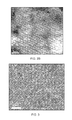
- FIG. 3 shows an scanning electron microscopy (SEM) image of a DC hot pressed sample corresponding to Yb 0.35 Co 4 Sb 12 .
- SEM scanning electron microscopy
- the SEM indicates that the average grain size was about 200 nm to about 300 nm.
- the clear facets show that the grains were well crystallized.
- the SEM image also shows that the crystallized grains were closely packed, implying a high volume mass density consistent with the volume mass density measurement of around 7.6 g/cm 3 , which is about the theoretical density of the composition.
- FIG. 5 a shows a low magnification TEM image of a sample with the composition Yb 0.35 Co 4 Sb 12 after DC hot pressing the sample.
- the image indicates that the grains are about several hundred nanometers in size, consistent with the SEM observation.
- the high resolution TEM image shown in FIG. 5 b confirms the excellent crystallinity, clean grain boundary, and large angle grain boundary.
- the excellent crystallinity and clean grain boundary typically are needed for good electrical transport properties, whereas the large angle grain boundary can potentially benefit phonon scattering.
- Table I shows the nominal compositions of the various samples and their measured properties at about 25° C.
- two samples (marked with *) as prepared and characterized in Nolas et al., J. Appl, Phys. 77, 1855 (2000) are also listed for comparison.
- the tested samples show a much higher electrical conductivity vis-à-vis Nolas et al.'s samples.
- the carrier concentrations for Yb x Co 4 Sb 12 are in a linear relation with the Yb filling value x.
- the Hall mobilities drop with higher Yb filling fraction.
- the carrier concentration increase is much larger that the carrier mobility decrease, which is why the electrical conductivity increases with increasing Yb doping.
- FIGS. 7 a - 7 d The measured and calculate temperature dependent thermoelectric properties of the Yb x Co 4 Sb 12 samples are plotted in FIGS. 7 a - 7 d .
- All samples have negative Seebeck coefficients ( FIG. 7 b ), indicating that electrons are the dominant carriers.
- FIG. 7 a all samples show metallic electrical conducting behavior whereby ⁇ drops with increasing temperature. Also ⁇ increases with increasing Yb content. Samples with different Yb content show a similar temperature dependence trend for the Seebeck coefficient from room temperature to 550° C., with the maximum Seebeck coefficient at about 550° C. ( FIG. 7 b ).
- the absolute value of the Seebeck coefficient decreases with increasing x at the same temperature, consistent with the electrical conductivity increases with increasing values of x.
- the thermal conductivity of the samples is shown in FIG. 7 c .
- the thermal conductivity values decrease with temperature and reach a minimum at 300° C. and then increases rapidly with temperature.
- the thermal conductivity keeps rising all the way from room temperature to 550° C.
- Increases in Yb content increase the electron contribution to the total thermal conductivity.
- more Yb can decrease the lattice contribution.
- Yb 0.35 Co 4 Sb 12 has an optimized lowest thermal conductivity with a minimum of 2.7 W/m ⁇ K, which leads to the optimal ZT profile.
- FIG. 7 d shows the temperature dependent ZT from room temperature to 550° C.
- the ZT value increases with temperature and reaches a maximum at around 550° C.
- the highest ZT is observed for the Yb 0.35 Co 4 Sb 12 sample with its maximum value of about 1.2 occurring at 550° C. This is about a 30% improvement in ZT value relative to state-of-the-art commercial n-type Co 4 Sb 12 .
- Samples of Co 4 Sb 12 -based n-type materials were prepared and tested having various amounts of ytterbium, neodymium, and lanthanum.
- samples of Co 4 Sb 12 -based n-type materials were prepared and tested having two types of filler atoms: one being ytterbium and the other being one of the other rare earth elements (e.g., neodymium, lanthanum) or a Group IIA element (e.g., barium).
- Samples were prepared by simultaneously ball milling elemental bulk materials of the appropriate constituents into particulates, where the bulk materials had a stoichiometry similar to the desired final material. Ball-milling resulted in the formation of nanoparticles having a size from about 1 nm to about 100 nm.
- the particulates were consolidated using a DC hot press, as described in Experimental Set 1, using similar parameters.
- the thermoelectric properties of the various samples were measured using the techniques and equipment described in Experimental Set 1.
- FIGS. 8 a - 8 f The comparative thermoelectric properties of the some of the various samples are shown in FIGS. 8 a - 8 f .
- FIGS. 8 a - 8 d graph the resistivity, Seebeck coefficient, power factor, and thermal conductivity, respectively, as a function of temperature for three samples: La 0.3 Co 4 Sb 12 , Nd 0.3 Co 4 Sb 12 , and Yb 0.3 Co 4 Sb 12 .
- the lattice thermal conductivity as a function of temperature is shown in FIG. 8 e
- ZT is plotted as a function of temperature for all three samples in FIG.
- graphs 810 a , 820 a , 830 a , 840 a , 850 a , 860 a correspond to a La 0.3 Co 4 Sb 12 sample
- graphs 810 b , 820 b , 830 b , 840 b , 850 b , 860 b correspond to a Nd 0.3 Co 4 Sb 12 sample
- graphs 810 c , 820 c , 830 c , 840 c , 850 c , 860 c correspond to a Yb 0.3 Co 4 Sb 12 sample.
- the neodymium-doped sample generally has a larger magnitude Seebeck coefficient
- the substantially lower lattice thermal conductivity of the ytterbium-doped sample leads to the best ZT values of the three samples at the tested temperatures.
- FIGS. 9 a - 9 f Comparative thermoelectric properties of some dual filler type samples are shown in FIGS. 9 a - 9 f .
- FIGS. 9 a - 9 d graph the resistivity, Seebeck coefficient, power factor, and thermal conductivity, respectively, as a function of temperature for three samples having two types of filler atoms (La 0.1 Yb 0.3 Co 4 Sb 12 , Ce 0.03 Yb 0.3 Co 4 Sb 12 , and Ba 0.1 Yb 0.3 Co 4 Sb 12 ) and a sample of Yb 0.3 Co 4 Sb 12 .
- the lattice thermal conductivity as a function of temperature is shown in FIG. 9 e
- ZT is plotted as a function of temperature for all three samples in FIG. 9 f .
- graphs 910 a , 920 a , 930 a , 940 a , 950 a , 960 a correspond to a La 0.1 Yb 0.3 Co 4 Sb 12 sample
- graphs 910 b , 920 b , 930 b , 940 b , 950 b , 960 b correspond to a Ce 0.03 Yb 0.3 Co 4 Sb 12 sample
- graphs 910 c , 920 c , 930 c , 940 c , 950 c , 960 c correspond to a Ba 0.1 Yb 0.3 Co 4 Sb 12 sample
- graphs 910 d , 920 d , 930 d , 940 d , 950 d , 960 d correspond to a Yb 0.3 Co 4 Sb 12 sample.
- the best results for the ZT values appears to be associated with the sample utilizing both barium and ytterbium as fill
- Samples of p-type skutterudite-based materials were prepared with filler atoms of one or more of cerium, ytterbium, neodymium, and lanthanum.
- the samples tested had the following stoichimetries: NdFe 3.5 Co 0.5 Sb 12 , Nd 0.9 Fe 3.5 Co 0.5 Sb 12 , CeFe 3.5 Co 0.5 Sb 12 , LaFe 3.5 Co 0.5 Sb 12 , YbFe 3.5 Co 0.5 Sb 12 , and La 0.9 Yb 0.1 Fe 3.5 Co 0.5 Sb 12 .
- Samples were prepared by loading the individual elements of each desired sample in the correct stoichiometric ratio into a high energy Spex ball milling jar.
- the starting materials were grinded for 15 to 25 hours to form small particles.
- the particles were compacted into a disk using a DC hot press.
- the conditions of pressing were to hold the sample at 600° C. for 5 minutes then for 2 minutes at 700° C. at a constant pressure of 20-80 MPa.
- the individual samples were annealed at 550° C. for about 2 hours in a flowing argon environment.
- TEM and SEM imaging was performed on the powder and consolidated samples, along with x-ray diffraction.
- the thermoelectric properties of the various samples were measured using the techniques and equipment described in Experimental Set 1.
- FIGS. 10 a and 10 b present two magnifications of TEM images of a ball-milled sample of starting materials having a stoichiometry ratio consistent with CeFe 3.5 Co 0.5 Sb 12 after 20 hours of ball milling.
- the bar in the lower left of FIG. 10 a corresponds with a length of 20 nm
- the bar in the lower left of FIG. 10 b corresponds with a length of 5 nm.
- X-ray diffraction analysis on the ball-milled powder indicated the powder was not alloyed. Using the Scherrer equation, a particle size of about 15 nm was calculated, in generally good agreement with the TEM images.
- FIGS. 11 a and 11 b present a SEM image and a TEM image, respectively, of the CeFe3 5 Co 0.5 Sb 12 sample after DC hot pressing. In conjunction with x-ray diffraction analysis done on the consolidated sample, the results indicated alloying occurred during the hot press. An average grain size of about 91 nm was calculated from the Scherrer equation, consistent with what is shown in the imaging.
- FIGS. 12 a - 12 e present graphs of the comparative thermoelectric properties of three NdFe 3.5 Co 0.5 Sb 12 samples. Each sample ball-milled for a different amounts of time, either 15, 20, or 25 hours.
- FIGS. 12 a - 12 d present graphs of the electrical conductivity, Seebeck coefficient, the product of the power factor and temperature, and thermal conductivity, respectively, as a function of temperature for each of the three different ball-milled samples.
- FIG. 12 e presents a comparative graph of the ZT value as a function of temperature for the three samples. In general, the longer ball milled samples result in a higher ZT value, which appears to generally peak at about 475° C.
- FIGS. 13 a - 13 e present graphs of the thermoelectric properties of four ReFe 3.5 Co 0.5 Sb 12 samples ball-milled for 20 hours, where, for individual samples, Re is one of lanthanum, neodymium, cerium, and ytterbium.
- FIGS. 13 a - 13 d present graphs of the electrical conductivity, Seebeck coefficient, the product of the power factor and temperature, and thermal conductivity, respectively, as a function of temperature for each of the four types of different filler atom samples.
- FIG. 13 e presents a comparative graph of the ZT value as a function of temperature for the samples. In general, the neodymium doped samples exhibited the best ZT properties of the four tested dopants.
- FIGS. 14 a - 14 e present the comparative thermoelectric properties of a NdFe 3.5 Co 0.5 Sb 12 sample and a Nd 0.9 Fe 3.5 Co 0.5 Sb 12 sample, each ball-milled for 15 hours.
- FIGS. 14 a - 14 d present graphs of the electrical conductivity, Seebeck coefficient, the product of the power factor and temperature, and thermal conductivity, respectively, as a function of temperature for each of the different neodymium-doped samples.
- FIG. 14 e presents a comparative graph of the ZT value as a function of temperature for the samples. In general, the lower neodymium doped sample exhibited better ZT properties.
- FIGS. 15 a - 15 e present the comparative thermoelectric properties of a LaFe 3.5 Co 0.5 Sb 12 sample and a La 0.9 Yb 0.1 Fe 3.5 Co 0.5 Sb 12 sample.
- FIGS. 15 a - 15 d present graphs of the electrical conductivity, Seebeck coefficient, the product of the power factor and temperature, and thermal conductivity, respectively, as a function of temperature for each of the different lanthanum-doped samples.
- FIG. 15 e presents a comparative graph of the ZT value as a function of temperature for the samples. The sample without ytterbium exhibited better ZT properties.
Abstract
Description
ReFe4-yMySb˜12
where Re is at least one of a rare earth element and a Group IIA element (e.g., barium), M is cobalt or nickel or combinations of them with other elements, and y is zero or a positive number no greater than 4. For instance, the p-type material can include a composition consistent with the formula ReFe3.5Co0.5Sb˜12, where Re is any one of neodymium, cerium, lanthanum, or ytterbium.
RezMyCo4-ySb˜12
where Re is at least one of a rare earth element and a Group IIA element, M is a metal, y is zero or a positive number no greater than 4; and z is a positive number no greater than 1. For example, the thermoelectric material can include a composition consistent with a formula: RezCo˜4Sb˜12, where z is a number between about 0.2 and about 1, and Re is at least one of cerium, neodymium, lanthanum, barium, and ytterbium. In another example, the thermoelectric material comprises a n-type composition consistent with a formula: Re1Z1Re2Z2Co˜4Sb˜12, where Z1 and Z2 are each independently a number between about 0.2 and about 1 with a sum of Z1 and Z2 not greater than about 1, and Re1 and Ret are each independently at least one of cerium, neodymium, lanthanum, barium, and ytterbium. In yet another example, the thermoelectric material comprises a composition consistent with a formula: YbzMyCo4-ySb12, where z is any number between about 0.2 and about 1, and y is optionally zero.
RezCo4-xMxSb12-yChy,
where x has a value in a range from 0 to 4, which includes the possibilities of x=0 and x=4; y has a value in a range from 0 to 12, which includes the possibilities of y=0 and y=12; z has a value of zero or a positive number no greater than about 2 (e.g., about 1, 0.9, 0.8, 0.7, 0.6, or 0.5); Re is a filling atom; M is a transitional metal required by charge compensation; and Ch is a Group VA atom such as antimony or an atom in close proximity to antimony such as tellurium.
Re1wRe2xFeyCo4-ySb˜12
where w and x each have positive values greater than or equal to zero, optionally their sum is less than about a selected value (e.g., 2 or 1); y has a positive value no greater than 4; Re1 is one type of filler atom (e.g., a rare earth atom); and Re2 is another type of filler atom different than Re1, which can be another rare earth atom or a Group IIA atom (e.g., barium). Of course, other Group VA atoms can be substituted for antimony, and other variations of a skutterudite-based material having multiple types of filler atoms and/or metal atoms forming the cubic sublattice are also possible.
RezMyCa4-ySb12
where Re is a rare earth element (e.g., lanthanum, cerium, ytterbium, neodymium, or combinations thereof) or a Group IIA element (e.g., barium, calcium, etc., or combinations thereof); M is a metal (e.g., iron, nickel, or others); y is zero or a positive number no larger than 4; and z is a value greater than zero. In some instances, z is no greater than about 1. In some instances, z has a value greater than about 0.2 or greater than about 0.3. As well, z can also have an upper limit no greater than about 0.5 in some instances. In some embodiments, these potential values of z can be applied when y is substantially zero. In particular embodiments, Re is any one of lanthanum, ytterbium, and neodymium, or Re is ytterbium. In other embodiments, two or more types of filler atoms can be used, for example:
Re1z1Re2z2MyCo4-ySb12
where z1 and z2 each have positive values such that the sum of z1 and z2 is no greater than about 1 or about 0.5. In some instances, y can be about 2. In some instances using multiple types of filler atoms, one type of atom is ytterbium, and optionally another type is barium.
RezFe4-xMxSb˜12
where Re is a rare earth element (e.g., lanthanum, cerium, ytterbium, or neodymium or combinations thereof) or a Group IIA element (e.g., barium, etc.); M is cobalt or nickel or combinations of them with other elements; x is 0 or a positive number no greater than 4; and z is any positive number less than 1 (including zero). For instance, in some embodiments, z is in a range from about 0.05 to about 1, and x is about 0.5; in a particular embodiment, Re is neodymium. As well, multiple types of filler atoms can be utilized, for example materials having a stoichiometry consistent with:
Re1z1Re2z2Fe4-xMxSb˜12
where z1 and z2 each have positive values such that the sum of z1 and z2 is no greater than about 1.
| TABLE I | ||||
| Electrical | Seebeck | Lattice Thermal | ||
| Conductivity | Coefficient | Conductivity | ||
| Composition | (105 S/m) | (μV/K) | (W/m K) | ZT |
| Yb0.066Co4Sb12* | 0.48 | −186 | 4.7 | 0.09 |
| Yb0.19Co4Sb12* | 1.64 | −141 | 2.6 | 0.26 |
| Yb0.3Co4Sb12 | 1.99 | −137 | 1.52 | 0.38 |
| Yb0.35Co4Sb12 | 2.13 | −130 | 1.35 | 0.37 |
| Yb0.4Co4Sb12 | 2.34 | −120 | 1.21 | 0.35 |
| Yb0.5Co4Sb12 | 2.54 | −108 | 1.08 | 0.30 |
Claims (21)
Priority Applications (1)
| Application Number | Priority Date | Filing Date | Title |
|---|---|---|---|
| US12/990,268 US8883047B2 (en) | 2008-04-30 | 2009-04-30 | Thermoelectric skutterudite compositions and methods for producing the same |
Applications Claiming Priority (4)
| Application Number | Priority Date | Filing Date | Title |
|---|---|---|---|
| US4927308P | 2008-04-30 | 2008-04-30 | |
| US4960908P | 2008-05-01 | 2008-05-01 | |
| PCT/US2009/042327 WO2009135013A2 (en) | 2008-04-30 | 2009-04-30 | Thermoelectric skutterudite compositions and methods for producing the same |
| US12/990,268 US8883047B2 (en) | 2008-04-30 | 2009-04-30 | Thermoelectric skutterudite compositions and methods for producing the same |
Publications (2)
| Publication Number | Publication Date |
|---|---|
| US20110108778A1 US20110108778A1 (en) | 2011-05-12 |
| US8883047B2 true US8883047B2 (en) | 2014-11-11 |
Family
ID=41255804
Family Applications (1)
| Application Number | Title | Priority Date | Filing Date |
|---|---|---|---|
| US12/990,268 Expired - Fee Related US8883047B2 (en) | 2008-04-30 | 2009-04-30 | Thermoelectric skutterudite compositions and methods for producing the same |
Country Status (2)
| Country | Link |
|---|---|
| US (1) | US8883047B2 (en) |
| WO (1) | WO2009135013A2 (en) |
Families Citing this family (9)
| Publication number | Priority date | Publication date | Assignee | Title |
|---|---|---|---|---|
| US10751801B2 (en) * | 2013-11-22 | 2020-08-25 | The Government Of The United States Of America, As Represented By The Secretary Of The Navy | Bulk monolithic nano-heterostructures and method of making the same |
| CN102373348B (en) * | 2010-08-20 | 2013-10-16 | 中国科学院上海硅酸盐研究所 | P-type skutterudite material and preparation method thereof |
| US9673369B2 (en) | 2012-07-06 | 2017-06-06 | Board Of Trustees Of Michigan State University | Thermoelectric materials based on tetrahedrite structure for thermoelectric devices |
| CN103132149B (en) * | 2013-03-19 | 2015-06-10 | 河南工业大学 | Preparation method of skutterudite nano material |
| WO2015003157A1 (en) * | 2013-07-03 | 2015-01-08 | Board Of Trustees Of Michigan State University | Thermoelectric materials based on tetrahedrite structure for thermoelectric devices |
| US20160035954A1 (en) * | 2014-07-29 | 2016-02-04 | GM Global Technology Operations LLC | Thermoelectric performance of calcium and calcium-cerium filled n-type skutterudites |
| JP6567847B2 (en) * | 2015-03-19 | 2019-08-28 | 古河機械金属株式会社 | Thermoelectric conversion material, thermoelectric conversion element, thermoelectric conversion module, thermoelectric power generation device, thermoelectric conversion system, and method of manufacturing thermoelectric conversion material |
| KR102122573B1 (en) | 2017-03-09 | 2020-06-12 | 주식회사 엘지화학 | Compound semiconductors and their application |
| JP2018157002A (en) * | 2017-03-16 | 2018-10-04 | 古河機械金属株式会社 | Thermoelectric conversion material |
Citations (10)
| Publication number | Priority date | Publication date | Assignee | Title |
|---|---|---|---|---|
| US5929351A (en) * | 1997-04-23 | 1999-07-27 | Matsushita Electric Industrial Co., Ltd. | Co-Sb based thermoelectric material and a method of producing the same |
| US5994639A (en) | 1997-03-25 | 1999-11-30 | The State Of Oregon Acting By And Through The State Board Of Higher Education On Behalf Of The University Of Oregon | Thermodynamically metastable skutterudite crystalline-structured compounds |
| US6207886B1 (en) * | 1998-06-30 | 2001-03-27 | Matsushita Electric Industrial Co., Ltd. | Skutterudite thermoelectric material thermoelectric couple and method of producing the same |
| US6207888B1 (en) * | 1997-10-10 | 2001-03-27 | Marlow Industries, Inc. | Semiconductor materials with skutterudite type crystal lattice structures optimized for selected thermoelectric properties and methods of preparation |
| US20020176815A1 (en) * | 1994-01-28 | 2002-11-28 | General Motors Corporation, A Delaware Corporation | Thermoelectric devices based on materials with filled skutterudite structutres |
| US20060053969A1 (en) * | 2002-11-28 | 2006-03-16 | Takashi Harada | Thermoelectric material and method for producing same |
| US20060176815A1 (en) | 2005-02-04 | 2006-08-10 | Picot Carol M | Method for reverse link overload control in a wireless communication system |
| WO2006106116A2 (en) | 2005-04-06 | 2006-10-12 | Centre National De La Recherche Scientifique (Cnrs) | Making thermoelectric materials by mechanosynthesis |
| US20080202575A1 (en) | 2004-10-29 | 2008-08-28 | Massachusetts Institute Of Technology (Mit) | Methods for high figure-of-merit in nanostructured thermoelectric materials |
| US7465871B2 (en) | 2004-10-29 | 2008-12-16 | Massachusetts Institute Of Technology | Nanocomposites with high thermoelectric figures of merit |
-
2009
- 2009-04-30 US US12/990,268 patent/US8883047B2/en not_active Expired - Fee Related
- 2009-04-30 WO PCT/US2009/042327 patent/WO2009135013A2/en active Application Filing
Patent Citations (11)
| Publication number | Priority date | Publication date | Assignee | Title |
|---|---|---|---|---|
| US20020176815A1 (en) * | 1994-01-28 | 2002-11-28 | General Motors Corporation, A Delaware Corporation | Thermoelectric devices based on materials with filled skutterudite structutres |
| US5994639A (en) | 1997-03-25 | 1999-11-30 | The State Of Oregon Acting By And Through The State Board Of Higher Education On Behalf Of The University Of Oregon | Thermodynamically metastable skutterudite crystalline-structured compounds |
| US5929351A (en) * | 1997-04-23 | 1999-07-27 | Matsushita Electric Industrial Co., Ltd. | Co-Sb based thermoelectric material and a method of producing the same |
| US6207888B1 (en) * | 1997-10-10 | 2001-03-27 | Marlow Industries, Inc. | Semiconductor materials with skutterudite type crystal lattice structures optimized for selected thermoelectric properties and methods of preparation |
| US6207886B1 (en) * | 1998-06-30 | 2001-03-27 | Matsushita Electric Industrial Co., Ltd. | Skutterudite thermoelectric material thermoelectric couple and method of producing the same |
| US20060053969A1 (en) * | 2002-11-28 | 2006-03-16 | Takashi Harada | Thermoelectric material and method for producing same |
| US20080202575A1 (en) | 2004-10-29 | 2008-08-28 | Massachusetts Institute Of Technology (Mit) | Methods for high figure-of-merit in nanostructured thermoelectric materials |
| US7465871B2 (en) | 2004-10-29 | 2008-12-16 | Massachusetts Institute Of Technology | Nanocomposites with high thermoelectric figures of merit |
| US20060176815A1 (en) | 2005-02-04 | 2006-08-10 | Picot Carol M | Method for reverse link overload control in a wireless communication system |
| WO2006106116A2 (en) | 2005-04-06 | 2006-10-12 | Centre National De La Recherche Scientifique (Cnrs) | Making thermoelectric materials by mechanosynthesis |
| US20090208364A1 (en) * | 2005-04-06 | 2009-08-20 | Centre National De La Recherche Scientifique (Cnrs) | Making Thermoelectric Materials by Mechanosynthesis |
Non-Patent Citations (4)
| Title |
|---|
| Bertini et al. Nanostructured Co1-xNixSb3 skutterudites: Synthesis, thermoelectric properties, and theoretical modeling. Journal of Applied Physics. vol. 93, No. 1. Jan. 2003. * |
| International Preliminary Report, dated Nov. 11, 2010, PCT/US2009/042327. |
| International Search Report and Written Opinion, dated Dec. 30, 2009, PCT/US2009/042327. |
| Nolas et al., High figure of merit in partially filled ytterbium skutterudite materials. Applied Physics Letters. 2000, vol. 77, issue 12, pp. 1855-1857. |
Also Published As
| Publication number | Publication date |
|---|---|
| WO2009135013A2 (en) | 2009-11-05 |
| WO2009135013A3 (en) | 2010-02-18 |
| WO2009135013A8 (en) | 2010-11-18 |
| US20110108778A1 (en) | 2011-05-12 |
Similar Documents
| Publication | Publication Date | Title |
|---|---|---|
| US8883047B2 (en) | Thermoelectric skutterudite compositions and methods for producing the same | |
| US8865995B2 (en) | Methods for high figure-of-merit in nanostructured thermoelectric materials | |
| Li et al. | Enhanced mid-temperature thermoelectric performance of textured SnSe polycrystals made of solvothermally synthesized powders | |
| JP5329423B2 (en) | A method for high explicit numbers in thermoelectric materials with nanostructures | |
| Zhu et al. | Increased phonon scattering by nanograins and point defects in nanostructured silicon with a low concentration of germanium | |
| Saleemi et al. | Synthesis, processing, and thermoelectric properties of bulk nanostructured bismuth telluride (Bi 2 Te 3) | |
| Wang et al. | High-performance Ag0. 8Pb18+ xSbTe20 thermoelectric bulk materials fabricated by mechanical alloying and spark plasma sintering | |
| Wang et al. | High performance n-type (Bi, Sb) 2 (Te, Se) 3 for low temperature thermoelectric generator | |
| Zou et al. | Synthesis and thermoelectric properties of fine-grained FeVSb system half-Heusler compound polycrystals with high phase purity | |
| Zhang et al. | Thermoelectric and transport properties of nanostructured Bi2Te3 by spark plasma sintering | |
| JP2016529699A (en) | Thermoelectric materials based on tetrahedral copper ore structure for thermoelectric elements | |
| WO2012138979A2 (en) | Thermoelectric materials and methods for synthesis thereof | |
| Bali et al. | Thermoelectric properties of PbTe with encapsulated bismuth secondary phase | |
| Cha et al. | Effect of La3+ substitution on the structural and thermoelectric properties of Ca3-xLaxCo4O9+ δ | |
| Nagarjuna et al. | Grain refinement to improve thermoelectric and mechanical performance in n-type Bi2Te2. 7Se0. 3 alloys | |
| Kuo et al. | Thermoelectric properties of fine-grained PbTe bulk materials fabricated by cryomilling and spark plasma sintering | |
| Falkenbach et al. | Thermoelectric properties of nanostructured bismuth-doped lead telluride Bi x (PbTe) 1− x prepared by co-ball-milling | |
| KR20120050905A (en) | Doped bi2te3-based thermoelectric material and preparing method of the same | |
| Yoon et al. | Effects of Ni and carbon-coated Ni addition on the thermoelectric properties of 25Bi2Te3+ 75Sb2Te3 base composites | |
| US9419196B2 (en) | Oxide nanoparticle-dispersed, chalcogenide-based, and phase-separated composite thermoelectric material | |
| US9076567B2 (en) | Reduced oxides having large thermoelectric ZT values | |
| Paul et al. | Grain structure induced thermoelectric properties in PbTe nanocomposites | |
| US20140186209A1 (en) | Thermoelectric skutterudite compositions and methods for producing the same | |
| US10283690B2 (en) | Formation of P-type filled skutterudite by ball-milling and thermo-mechanical processing | |
| KR102046142B1 (en) | Thermoelectric powder and materials with improved thermostability and manufacturing methods thereof |
Legal Events
| Date | Code | Title | Description |
|---|---|---|---|
| AS | Assignment |
Owner name: MASSACHUSETTS INSTITUTE OF TECHNOLOGY, MASSACHUSET Free format text: ASSIGNMENT OF ASSIGNORS INTEREST;ASSIGNORS:CHEN, GANG;HAO, QING;REEL/FRAME:025426/0432 Effective date: 20090609 Owner name: TRUSTEES OF BOSTON COLLEGE, MASSACHUSETTS Free format text: ASSIGNMENT OF ASSIGNORS INTEREST;ASSIGNORS:REN, ZHIFENG;YANG, JIAN;YAN, XIAO;AND OTHERS;SIGNING DATES FROM 20090618 TO 20101111;REEL/FRAME:025426/0773 Owner name: MASSACHUSETTS INSTITUTE OF TECHNOLOGY, MASSACHUSET Free format text: ASSIGNMENT OF ASSIGNORS INTEREST;ASSIGNORS:CHEN, GANG;HAO, QING;REEL/FRAME:025426/0582 Effective date: 20090609 |
|
| AS | Assignment |
Owner name: NATIONAL SCIENCE FOUNDATION, VIRGINIA Free format text: CONFIRMATORY LICENSE;ASSIGNOR:MASSACHUSETTS INSTITUTE OF TECHNOLOGY;REEL/FRAME:028231/0042 Effective date: 20120301 |
|
| AS | Assignment |
Owner name: ENERGY, UNITED STATES DEPARTMENT OF, DISTRICT OF C Free format text: CONFIRMATORY LICENSE;ASSIGNOR:MASSACHUSETTS INSTITUTE OF TECHNOLOGY;REEL/FRAME:029435/0201 Effective date: 20120301 |
|
| FEPP | Fee payment procedure |
Free format text: PAYOR NUMBER ASSIGNED (ORIGINAL EVENT CODE: ASPN); ENTITY STATUS OF PATENT OWNER: SMALL ENTITY |
|
| FEPP | Fee payment procedure |
Free format text: MAINTENANCE FEE REMINDER MAILED (ORIGINAL EVENT CODE: REM.) |
|
| LAPS | Lapse for failure to pay maintenance fees |
Free format text: PATENT EXPIRED FOR FAILURE TO PAY MAINTENANCE FEES (ORIGINAL EVENT CODE: EXP.); ENTITY STATUS OF PATENT OWNER: SMALL ENTITY |
|
| STCH | Information on status: patent discontinuation |
Free format text: PATENT EXPIRED DUE TO NONPAYMENT OF MAINTENANCE FEES UNDER 37 CFR 1.362 |
|
| FP | Lapsed due to failure to pay maintenance fee |
Effective date: 20181111 |