| Winter-21 | Spring-22 | Summer-22 | Fall-22 | |
| Spring-23 | Summer-23 | Fall-23 | Winter-23 | |
| Spring-24 |
[18-OCT-23] The Implantable Stimulator-Transponder (A3041) receives commands through its crystal radio, interprets these commands and executes them with its own embedded microprocessor, applies stimuli to its two stimulus leads, transmits a synchronizing telemetry signal upon command, and reports on its own battery voltage. All versions of the A3014 stimulator are powered by CR-series lithium primary cell. These batteries are not rechargeable, but provide long life and ample stimulus current. We ship the A3041 with a magnet attached. The magnet that keeps it in its sleep state, which minimises its current consumption. When we remove the magnet, the A3041 enters its wake state. When the A3041 receives a command, it becomes active. If instructed to do so, the A3041 will generate a stimulus consisting of electrical pulses of current applied to its stimulation leads. The magnitude of the current, the duration of the pulses, their period, their quantity, as well as whether they should be regular or random, are all specified in a single command. By uploading user-programs through its crystal radio and into the memory of its microprocessor, we can configure the A3041 to provide arbitrarily complex stimuli that suit our own experiment.

The A3041A-DD provides two pins on the ends of its stimulus leads that we can connect to an Implantable Light-Emitting Diode (ILED) to provide optogenetic stimulation, or to a bipolar electrode to provide direct electrical stimulation. All versions of the A3041 generate stimuli by connecting a current source to its stimulus leads. The current source is programmable by a current code. The A3041A provides currents from 200 μA to 10 mA. The maximum voltage the A3041 can apply to its stimulus leads is fixed for each version of the device. The A3041A can deliver at most 3.3 V. Other voltage options are 3.0 V and 5.0 V.
| Property | Value |
|---|---|
| Volume of Implant | 0.95 ml |
| Mass of Implant | 1.7 g |
| Outer Dimensions | 14 mm dia, 6.5 mm thick |
| Battery Type | CR1220 |
| Nominal Battery Capacity | 40 mAhr |
| High Power Stimulus Life | 40 hr |
| Low Power Stimulus Life | 240 hr |
| Sleep Current | 2.2 μA |
| Sleep Control | sleeps in magnetic field |
| Wake Current | 5.5 μA |
| Active Current | 140 μA @ 37°C |
| Stimulus Voltage | 3.3 V |
| Stimulus Current Range | 200 μA to 10 mA |
| Pulse Length Range | 2 ms to 60 s |
| Pulse Period Range | 4 ms to 60 s |
| Stimulus Length Range | 1 to 60k pulses |
| Operating Range | 30 cm |
The operating range of the IST is the range from its command antenna for which reception of commands is ≥95%. We specify operating life for two reference stimuli. The high-power stimulus (HPS) is 5-mA pulses 10% of the time at 10 Hz. The high-power stimulus life is the number of hours an IST with a fresh battery can sustain the stimulus without pause. The low-power stimulus is 200 μA pulses 25% of the time at 10 Hz. The low-power stimulus life is the number of hours a fresh battery can provide the low-power stimulus. In Battery Life we provide rules for determining whether a particular battery can support a planned experiment.

The A3041 uses its antenna to receive wireless commands and to transmit wireless messages. We address each IST with its own unique four-byte identifier, which we record as a four-digit hexadecimal number on the device label. We transmit commands to an IST with a command transmitter such as the A3029. We control the command transmitter with the Stimulator Tool in our LWDAQ software. The IST can transmit acknowledgements, its version number, and battery measurements. It can identify itself in response to a multicast request. It will transmit a synchronizing signal that shows when its stimulus pulses occur. When the A3041 transmits its synchronizing signal, it uses a telemetry channel that we assign in the transmit command. All IST transmissions use our SCT telemetry system protocol. The commands they receive from the command transmitter use the same radio frequency, but a dramatically different protocol. The commands consist of slow, high-power pulses, while the transmissions consist of micropower, frequency-modulated bursts.

In addition to its buit-in functions, the A3041 allows us to upload our own programs to run on its embedded OSR8 microprocessor. These programs, written in the OSR8 assembly language, can be up to 2 KBytes long. By means of the user programs we can provide new and complex stimuli as required by particular experiments. See the Stimulator Tool manual for details of how to prepare and upload programs to the A3041 memory. The A3041's user program memory is volatile, so all programs are lost when the device deactivates into its wake or sleep states.
[29-NOV-23] Here are the versions of the A3041 we have defined so far. Each version has a letter that constrains the battery type, battery mounting, maximum voltage, current range, and maximum load. A high-power stimulus is 5-mA pulses with 10% duty cycle. A low-power stimulus is 200 μA pulses with 25% duty cycle.
| Version | Battery Type |
Battery Capacity (mAhr) |
Stim Voltage (V) |
Stim Current (mA) |
High Power Life (hr) |
Low Power Life (hr) |
Volume (ml) |
Mass (g) |
Wake (mo) |
|---|---|---|---|---|---|---|---|---|---|
| A3041A | CR1220 | 40 | 3.3 | 0.2-10 | 40 | 200 | 0.95 | 1.7 | 9 |
| A3041B | CR1616 | 60 | 3.3 | 0.2-10 | 60 | 300 | 1.2 | 2.3 | 14 |
| A3041C | CR1620 | 80 | 3.3 | 0.2-10 | 80 | 400 | 1.3 | 2.5 | 19 |
| A3041D | CR2032 | 200 | 3.3 | 0.2-10 | 200 | 1000 | 2.5 | 5.0 | 47 |
In the table, we give guaranteed battery life. Typical battery life is 10% greater. We can equip the A3041 with any of our flexible leads. By default, we use orange and purple B-Leads. These are 0.7 mm in diameter, contain a helix of stainless steel wire 450-μm in diameter, and have resistance 6.3 Ω/cm. These leads can be anything from 30 mm to 280 mm long. At the ends of the leads, we can have bares wire for delivering electrical stimulation, or pins to connect to depth electrodes or an implantable lamp. See our Catalog of Electrodes and our Implantable Lamp manual for details.
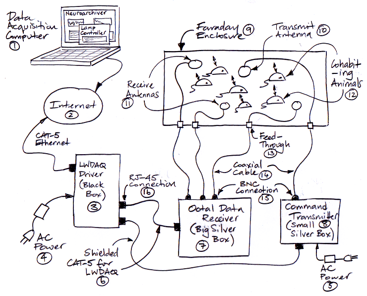
[08-OCT-23] At the moment, the only way to command the IST is with a Command Transmitter (A3029C) connected to a LWDAQ Driver (A2071E). We describe how to connect these devices, along with an Octal Data Receiver (A3027), in the Stimulator Tool manual. The Stimulator Tool manual also contains instructions on how to compose and upload your own programs to the IST so that it can implement specialized stimuli.
In the next year, the Telemetry Control Box (TCB-B16) will replace the A3029C, A3027E, and A2071E. The TCB-B16 will need only one Power over Ethernet (PoE) connection for power and communication. It will provide sixteen coaxial antennas that will receive telemetry signals and transmit commands to ISTs. With the TCB-B16, set-up is simpler: we put antennas wherever we need reception or transmission, and we can use any antenna alternately for reception and transmission. The TCB receives its power from the PoE connection, and all communication with the TCB takes place over the same PoE cable. The same LWDAQ Software with its Stimulator Tool operates the TCB using the same interface as for the older A3029C, A3027E, and A2071E system.
[29-NOV-23] The A3041's stimulus output is limited in both current and voltage: there is a maximum voltage it will apply to the stimulus leads and a maximum current it will allow to flow through the stimulus leads. The maximum voltage is a function of the boost converter we load onto the A3041 circuit. It can be 3.0 V, 3.3 V, or 5.0 V. In the case of the A3041A, the maximum voltage is 3.3 V. The current is controlled by a four-bit current code we select in Stimulator Tool. Its value can be 0-15. The magnitude of the current is inversely proportional to the value of a resistor on the circuit (See R6 S3041A_1). In the A3041A, the maximum current is a little under 10 mA, while the minimum is a little over 200 μA.

An ideal current source would deliver the same current to any load. But our current source is not ideal. If we short the stimulus pins together, the maximum current is 9.4 mA. If we connect an LED to the pins the stimulus pins, the maximum current is 5.5 mA. With the stimulus leads open circuit, there is no path for the stimulus current. The stimulus current sink applies the maximum voltage to the leads. With a white LED attached, the stimulus voltage is the forward voltage of the LED, which is roughly 2.9 V.

If we want to deliver 10 mA to an ILED at the end of 130-mm leads, the resistance of the B-Lead becomes significant. We have a total of 26 cm of 0.7-mm diameter B-Lead, so total resistance is 26 × 6.3 Ω/cm = 164 Ω. Our 10-mA current will drop 1.6 V. But the LED itself needs around 2.9 V, so our total stimulus voltage must be 4.5 V. We can use a 5.0-V version of the A3041. Another option is to use a 3.3-V version, but equip the stimulator with the low-resistance D-Lead instead. The D-Lead is made with thicker wire and wound with fewer coils per unit length. It is stiffer than the B-Lead, but its resistance is only 1.6 Ω/cm. A 3.3-V stimulator can drive 10 mA through a 2.9-V LED with 26 cm of D-Lead to deliver the current.
[18-OCT-23] Each battery has a nominal capacity, which is the amount of electrical charge it can deliver before it is exhausted. We express battery capacities in milliamp-hours (mAhr). One milliamp-hour of battery capacity will provide us with a cetain amount of sleep, wake, or stimulus. We use the following guidelines to estimate the battery capacity that will be consumed by our planned use of a stimulator. We define high-power stimulus to be 5 mA, 10% duty cycle, 10 Hz, and low-power stimulus as 200 μA, 25% duty cycle, 10 Hz. The device is awake when it is doing nothing except for awaiting a instructions.
| State | Consumption Rule |
|---|---|
| Sleeping (disabled by magnet) | 19 days per 1 mAhr |
| Waking (ready for commands) | 7 days per 1 mAhr |
| High-Power Stimulus (5 mA, 10%) | 1 hr per 1 mAhr |
| Low-Power Stimulus (0.2 mA, 25%) | 5 hr per 1 mAhr |
Example: We propose to implant ISTs in mice, administer an average of 20 high-power stimuli per day, each stimulus lasting for one minute, and continue doing so for six weeks. Our ISTs have been sitting on the shelf for two months with their magnets attached, sleeping. The sleep used 3 mAhr. We remove the magnets, and our ISTs wake up. We implant and begin our experiment. The device will be awake for six weeks, which will use 6 mAhr. We want to deliver 20 stim/day × 42 days × 1 min/stim = 14 hr of high-power stimulus, which uses another 14 mAhr of battery capacity. Our total is 23 mAhr. The CR1220 capacity is 40 mAhr. We have plenty of extra capacity in our battery to accommodate variation in the number of stimuli from one animal to the next.
We equip all our ISTs with CR-Series lithium primary cells that are specified for high-current and pulse operation, as is required by the stimulator. Lithium cells provide the highest charge density of all existing battery technologies, and of all types of lithium primary cell, the CR-Series cells made by Murata are the most tolerant of pulsed loads. The capacity of lithium batteries decreases significantly if we exceed their rated current. For each battery we provide a maximum current for which our battery life calculations will be accurate.
| Battery | Capacity (mAhr) |
Diameter (mm) |
Thickness (mm) |
Mass (g) | Capacity per Gram (mAhr/g) |
Max Cont Stimulus (mA) |
|---|---|---|---|---|---|---|
| CR1220 | 40 | 12.5 | 2.0 | 0.77 | 52 | 1.0 |
| CR1616 | 60 | 16 | 1.6 | 1.1 | 54 | 1.2 |
| CR1620 | 80 | 16 | 2.0 | 1.3 | 61 | 1.4 |
| CR2016 | 90 | 20 | 1.6 | 1.8 | 50 | 1.5 |
| CR2025 | 160 | 20 | 2.5 | 2.6 | 62 | 2.0 |
| CR2032 | 200 | 20 | 3.2 | 3.0 | 67 | 2.2 |
| CR2450 | 600 | 24.5 | 5.0 | 6.2 | 97 | 4.0 |
The voltage produced by these batteries is 2.9 V for most of the battery's life, provided the load is less than 100 μA. During a stimulus pulse, the battery voltage drops well below 2.9 V. If an A3041's battery voltage drops below 2.4 V, the circuit will shut down. The smallest battery that provides reliable operation of the A3041 is the CR1220 by Murata.

The IST can be in one of three states: sleep, wake and active. The IST sleeps when it has a magnet attached to its body. In sleep, it consumes 2.2 μA. Without a magnet, the IST is awake until it receives a command. While awake, the IST consumes 5.5 μA. When it receives a command, it activates, and remains active until it has completed all instructions. The IST's current consumption increases with stimulation current, pulse length, pulse frequency, synchronizing signal rate, and randomization. The cost of generating timing signals for pulses is 0.28 μA/PPS (microamp per pulse per second). The additional cost of randomizing the production of these pulses is 0.86 μA/PPS. The cost of synchronizing transmission is 0.22 μA/SPS (microamp per sample per second). The active current increases with temperature, see here. To account for this increase, we add a temperature-dependent correction to the active current. At 37°C, an active IST consumes roughly 40 μA more than it does at 25°C.

As we increase the current code, our stimulus current increases. As the stimulus current increases, so does the battery current. If our stimulus operates on a 10% duty cycle, the battery current drawn by the stimulus will be almost ten times smaller.

In a high-power stimulus we have 5 mA pulses with 10% duty cycle. The average stimulus current is 0.5 mA. The current drawing from the battery is higher than our stimulus current. During the pulses, battery current is 7.7 mA. If we deliver the high-power stimulus for ten hours, we draw 7.7 mA from the battery for one hour and 140 μA for nine hours. The high-power stimulus life is roughly one hour per milliamp-hour of nominal battery capacity. The average battery current during the high-power stimulus is ≈ 0.90 mA.

When it comes to determining the lifetime of other stimuli, we first make sure the average stimulus current, IAVE, is less than the maximum continuous stimulus current for our battery, IMAX. When we calculate the average stimulus current, we must do so over a one-second period. If we deliver 10-s pulses of 10 mA once every 100 s, we must regard this as IAVE = 10 mA for 10% of the time, which exceeds IMAX for all our batteries. But if we deliver 10-ms pulses of 10 mA once every 100 ms, IAVE = 1 mA, and this average current is tolerated by all our batteries. Provided that IAVE ≤ IMAX, we get 1 hr × 0.5 mA ÷ IAVE hours of our stimulus for each 1 mAhr of battery capacity. Here we are using the average stimulus current of our high-power stimulus as our reference point for scaling the stimulus lifetime.
Example: Our stimulus consists of 10-mA pulses, 30 ms at 10 Hz. Our average stimulus current is 3.0 mA. We need the CR2450 battery to provide such a stimulus. For 1 mAhr of battery capacity, we get 1/6 hr of stimulus. The battery has capacity 600 mAhr, so it can provide the stimulus for 100 hr.
[29-DEC-23] The A3041 functions are built around an OSR8 microprocessor. The firmware and software running in its logic chip are contained in a single GitHub repository P3041. The main program is ROM.asm. Through its crystal radio, the A3041 receives commands in the form of strings of instructions. Each instruction consists of an operation code, one or more operands, and one or more data bytes. The table below describes the instructions in detail.
| Opcode | Pneumonic | Name | Operands | Description |
|---|---|---|---|---|
| 0 | op_stop | Stimulus Stop | 0 | Stops the main program stimulus. |
| 1 | op_start | Stimulus Start | 8 | Defines and starts a main program stimulus. |
| 2 | op_xon | Synchronizing Signal | 2 | Start sync signal with frequency and channel. |
| 3 | op_xoff | Acknowledgement | 1 | Transmit acknowledgement with key. |
| 4 | op_batt | Report Battery Voltage | 0 | Measure and transmit battery voltage. |
| 5 | op_id | Announce Identity | 0 | All stimulators self-identify. |
| 6 | op_pgld | Load Program | 1 | Load a block of user program bytes. |
| 7 | op_pgon | Run Program | 0 | Run the user program. |
| 8 | op_pgoff | Halt Program | 0 | Halt the user program. |
| 9 | op_pgrst | Reset Load Pointer | 0 | Reset user program load location. |
| 10 | op_shdn | Shutdown | 0 | Deactivated the device, forcing it into wake state. |
| 11 | op_ver | Report Version | 0 | Transmit version number. |
A command consists of two ID bytes to specify the IST. The identifier 0xFFFF is the multicast ID. All ISTs will respond. We use the multicast ID to get all ISTs to identify themselves. Following the ID are the opcodes and their operands and data bytes. Last of all comes a two-byte checksum. We can see these bytes being listed before transmission in the text window of the Stimulator Tool when we have the Verbose box checked.
The IST can provide stimuli in one of two ways: a main-program stimulus or a user-program stimulus. The main program stimulus is entirely defined with five parameters: pulse length, pulse interval, number of pulses, pulse current, and randomize flag. The user program stimulus is defined by an OSR8 assembly program we upload to the stimulator. This program is subject to three restrictions: it executes once every 5 ms, it must not take more than 4 ms to execute, and its program size cannot exceed 4 KByte. Aside from these restrictions, the user program can implement any stimulus behavior.
To upload a user program, we use the Stimulator Tool's transmit panel, as described in User Programs. We prepare our user program in a text file containing OSR8 assembler. When we press Run Program, Stimulator Tool uploads and runs our program. It resets the program load location with op_pgrst. It uploads the program in one or more chunks of up to 255 bytes each using op_pgld instructions. This upload takes place at roughly 1 KByte/s. A 4-KByte program broken into 32 chunks of 128 bytes each will take roughly ten seconds to upload. Once the upload is complete, the Stimulator starts it running with op_pgon.
A user program can either halt itself, or run until the IST receives an op_off instruction. The Halt Program button in the Transmit Panel sends op_off to stop the program. The A3041 has no ability to remember a user program after it deactivates, so we must keep the device in its active state in order to remember a program. When we define a special stimulus, which we want to deliver upon command, the user-program should continue to run, waiting for a stimulus start command. When the IST receives a stimulus start, the five parameters of a main-program stimulus will be set, and the stimulus run flag will be set. The user program, seeing that a main program stimulus has commenced, disables the main program stimulus and begins its own stimulus. If the user program stimulus needs to be configured, it can use the five parameters uploaded to the IST with the main program stimulus start instruction.
The stimulus current is delivered by a bipolar transistor, 2SC6026. We deliver a current to the base and trust that the current through the collector of the transistor will be proportional to the base current. When we ask this transistor to deliver 10 mA with a base current of 50 μA, we need to allow at least 0.5 V collector-emitter voltage for the current to flow. With a 3.3-V power supply, we are left with only 2.8 V for an LED that requires 2.9 V, hence the reduced LED current for the higher current codes.
[28-JUN-22] The A3041 is equipped with a D-Type antenna: 30-mm stranded-steel thin loop used both for receiving commands and transmitting synchronizing signals, acknowledgements, and battery measurements. We transmit commands to the implant by turning on and off a 915-MHz power source. The implant's crystal radio generates a logic HI when the power at its antenna is greater than a threshold. It generates a logic LO otherwise. We construct the command out of a pattern of HI and LO levels. Implants like the IST are almost always inactive. Their logic chips are disabled. The command transmission begins with an initializing pulse that wakes up the implant and enables the logic chip.

The initializing pulse lasts for tI ≥5 ms. While the pulse endures, the crystal radio asserts OND, which powers up the logic chip. As soon as the logic chip has configured itself, it asserts OND itself. The configuration should take tPU < 3 ms so that the initializing pulse will endure for > 2 ms after configuration is complete. When the logic chip has seen ≥2 ms of the initializing pulse, it starts to monitors the state of RP (Radio Frequency Power) for the purpose of receiving command bytes. It samples RP on the rising edges of RCK, its 32.768 kHz oscillator. When it sees RP go LO it waits for a start bit, after which it records eight bits of a command byte followed by a stop bit. It waits for another start bit, and so on, until one of the stop bits extends for 5 ms, which indicates the end of the command. The implant can analyze the command bytes as they arrive, or it can analyze them later. If the command requires nothing of the implant, the implant will deactivate immediately.

In the photograph above we see the IST receiving a command on RP, then processing the command afterwards. The CPU reads the bytes out of the command memory one by one and executes them. When it's done, it clears CMDRDY.
[10-APR-24] The following files define the A3041 design. Note that we distribute all these files under the GNU Public License. Any design that incorporates any part of our work must itself be distributed under the same GNU Public License.
S3041A_1.gif: Crystal radio, logic, stimulator, version A.[14-NOV-23] The A3041AV1 assembly as received from our assembly house needs the following modifications.

The A3041AV2 will provide all the component changes in the modification list above. We will add R15 to the A3041AV2 by hand.
The A3041BV1 will power U6 from VS rather than VH. To make the A304101B printed circuit board for the A3041BV1, we must modify the A304101A like this:
[02-FEB-22] The A3041 will incorporate the following improvements compared to the A3036.

With CR1025's 30-mAhr capacity, we have 5000 hrs of wake life while implanted, ignoring stimulus current. Stimulus current we assume will be of order 2 mA for optogenetics, following our study of FCLEDs in mice, where 1-ms flashes of 15 mA was sufficient to cause response with blue light, so 10-ms flashes of 1.5 mA should be sufficient. Because the current is ten times lower than we expected when we designed the A3036, we can switch out the A3036's lipo battery for a CR-series coin cell with three times the capacity per unit volume, and low enough source resistance to supply the LCMXO2-1200ZE with its startup current, and a lamp with 10 mA. We will make sure the lamp does not turn on when the device powers up. We will include resistors to allow us to turn on the device with a jumper when we tune the crystal radio.
[10-FEB-22] We are wondering if we can use the crystal radio's split capacitor tuner to create a resonator at the same frequency, and so tune both transmit and receive frequencies at the same time during production of the A3041. We build the following circuit using an A3038X. According to our calculations, the tuner should provide a phase shift of close to 180° just above its resonant frequency. Combined with the phase shift through a single-stage amplifier, we might see oscillation near the resonant frequency.

In the tuner, we use the same inductors and capacitors as the A3038DM-E tuner. We start with R1 = 560 Ω and C2 = 10 pF. We connect a spectrometer to J1 and we connect J2 to an oscilloscope. The P output on J2 tells us the power at J1 in the range 50-6000 MHz. We use the spectrometer to measure frequency and stability of the peak.

With R1 = 560 Ω and C2 = 10 pF we adjust VC1 until our peak is at 905 MHz. Power is −20 dBm. With C2 increased to 100 pF we see 902 MHz −18 dBm. We drop R1 to 280 Ω and see 870 MHz −4 dBm. We adjust VC1 to get 917 MHz −10 dBm.
[14-FEB-22] Complete S3041_1 schematic. We have dropped the 10-μH, P1210 inductor used in the A3030E to a 4.7 μH P0805 inductor to save space, and anticipating that our output current will be no more than 10 mA. Our stimulus output switch is an NPN transistor driven by a low-pass filter. If we know the current gain of this transistor, and the cut-off frequency of the filter is much lower than the frequency of our drive square wave, we can vary the duty cycle of the square wave to control the stimulus current. Our sleep switch is a p-channel mosfet.
[18-FEB-22] We decide against double-use of the split-capacitor tuner. When we add up all the parts it requires, we get no reduction in board area compared to a MAX2624, and we introduce uncertainty into the design. We plan to embed an OSR8 microprocessor in the logic of the IST. Because we have an ADC dedicated to measuring battery voltage, we can use our OSR8 microprocessor to compensate for drop in battery voltage when driving the tuning input of the MAX2623 or MAX2624, having established the correct DAC output value for a known battery voltage. We now have all logic IO banks connected to VA, which simplifies our layout.
[25-MAR-22] Working on the layout of the A304101A, a 400-mil square (10.2 mm square) implant with two extensions, battery pads on the North and South edges rather than at the corners, built-in zig-zag antenna, test points for calibration and tuning. We will be using 8-mil via-in-pad between top and bottom layer pads, as well as 4-mil micro-vias from top layer to middle layer in the WLCSP-25 ball grid array (BGA), see here for layout description and here for the BGA pinout.
[28-MAR-22] The A304101AR1 layout is complete. The implant circuit is 400-mil square (10.2-mm square).
[07-APR-22] Our A304101A layout has passed DFM and final netlist checks. We are waiting for quotes. Digi-Key has no stock of MCP6541, but we have 200 pieces on cut tape. We identify LPV7215 by TI in SC-70-5 package as a drop-in replacement, but it's out of stock too. We have a draft version of the firmware A01 based upon P3035A11. We use the new OSR8V3 CPU, which allows us to change the process and program memory space easily with generic constants. Upon power-up, the Command Processor in Main.vhd looks for a start pulse on RP. When it sees a start pulse, it asserts OND with its own Command Processor Active (CPA) signal. It receives command bytes carried by RP and stores them in the Command Memory. When the command ends, due to lack of RP for the termination pulse length, if the checksum of the command is correct, the Command Processor asserts Command Ready (CMDRDY) and waits for Command Processor Reset (CPRST). The Command Processor will continue to assert OND with CPA until it is reset. The number of bytes it stored is available to the CPU at the command count locations. After power-up, the CPU must poll the command ready location. When it sees a command, it reads out and processes all the command bytes, except for the final two, which are the checksum. The CPU can then decide whether to assert OND through Device Active (DACTIVE) before writing to the Command Processor Reset location to restore the Command Processor, which will un-assert CPA. If the CPU has not set DACTIVE, the power will turn off.
In the A3041, the positive stimulus voltage is always driven while the device is active. As soon as VA is asserted, S+ pumps up to 3.3 V or 5.0 V, depending upon our choice of U6. For implantable lamps, we'll have 3.3 V connected to an LED with forward voltage 3.0 V. With ONL unasserted, the S− will float up to S+ immediately. We assert and un-assert the ONL signal with the Stimulus Current location. The ONL signal passes through R6 to drive C9 and the base of Q2. With 33 kΩ and 10 nF, the time constant of the low-pass filter formed by R6 and C9 is 330 μs. We will measure the current gain of Q2, 2SC6026MFV. Assume gain is 200, base-emitter drop 600 mV. With ONL set at VA = 2.6 V we have base current 60 μA and collector current 12 mA. If we are driving 50-Ω leads and a 3.0-V LED with 3.3 V we cannot deliver more than 6 mA, so Q2 will saturate and S− will be around 50 mV. If we modulate ONL, the current flowing into S− will be 12 mA multiplied by the duty cycle of ONL, provided the load does not restrict the current. If we want to deliver a 200-μA electrical stimulus in a 10-ms pulse at 1 Hz, we use the processor's 5 MHz boost clock speed to run a counter from 0 to 59 and assert ONL on count 0 only. We deliver 833 such pulses on ONL in the 10-ms stimulus pulse length.
The A3041 allows us to measure the regulated 1V2 power supply with respect to VA with an eight-bit ADC, U9. The CPU reads the ADC by writing to the sensor control register, which turns on the transmit clock and uses it to read the ADC in about 5 μs. The CPU can read the result in the battery monitor location. If this eight-bit value is x, the current value of VA is 1.2 × 255 / x, which the CPU can of course work out for itself. Having figured out the battery voltage, the CPU can adjust the value it uses on the 5-bit transmit frequency control DAC so as to compensate for variable battery voltage during the life of the device. In previous implants, we have used a regulated voltage for the I/O banks that drive the DAC, but in this case we simplified routing by using VA.
The A3041 auto-calibrates its own ring oscillator upon power up, just like the A3035, so we have TCK set to 5.0 MHz to within 5%. We still have to obtain a value for the transmit low frequency that we should apply to the transmit DAC for a reference battery voltage of 2.6 V, and put this in the software that runs on in the A3041's CPU. Or, we could transmit a calibration value to the A3041 with every command, having measured the center frequency of each one and stored the calibration value with the device identifier. Suppose we give the A3041 a twenty-four bit identifier for command reception. Each one will be unique, so we can keep calibration constants on-line and use them to calibrate the stimulator when it wakes up.
[13-JUN-22] Receive 10 of A3041AV1 assemblies, build B109535. We start with circuit No4. Connect external 2.7 V. Quiescent current 5.9 μA. Bring magnet near to activate U1 and we have 1.0 μA. We connect OND to VH. Current is 17 mA. We have VA=0.5V and 1V2=0V while VS=VH=2.7V. Current drawn from VA is 17 mA at 0.5V. While messing about with another circuit, we see the current drop to 4 mA and we are able to program the chip, but we program with P3035A code rather than P3041A. We are unable to re-program or to program the first board.
[15-JUN-22] We short U6-1 and U6-3 on No4 with tweezers, thus connecting VA to VH. We see 130 mA flowing into the board from our 2.7-V power supply. We program the logic chip while holding the tweezers in place. After programming, current remains 120 mA with VA=VH. We remove U9, no change. We remove U8, we now can apply jumper to OND-VH to turn on the board and we see 253 μA quiescent current, of which 81 μA is current through R8, so active current is 172 μA. Now switch to circuit No6, which we previously were able to program, but upon which we now see VA will not power up. We short VA to VH and see 20 mA. We program the logic chip. Now we see 1.8 μA sleep current, 6.5 μA wake current, and 251−81 = 170 μA active current. Our U8 on No4 must have been damaged.
Start work on firmware A03. We program No6 repeatedly without any difficulty. Our ROM.asm program, assembled to ROM.mem, runs on the OSR8V3 CPU. We have configured the CPU with 12-bit program and cpu memory addresses. The program memory is therefore 4 kBytes, all of which is provided by ROM. Variable and stack memory are 1 kByte from address 0 to 1023, stack is from 768 to 1008. The command memory, where commands received by the crystal radio are stored, is 1 kByte from 1024 to 2047. The control memory space is from 2048 to 3071. The V3 software generates a ramp at 128 SPS on Channel 55, completing the ramp every two seconds. It generates a pulse on TP1 during every sample transmission, a pulse on TP2 on every run through the main loop, RCK on TP3, as marked on silk screen, and TCK on TP4, as marked on silk screen. The stimulus power supply is always powered up while the device is active, and we measure it to be 3.3V as we vary the supply voltage from 2.2-2.8 V. Current consumption at 2.7V is 152 μA when active, 7.0 μA wake, 2.1 μA sleeping. We set up GitHub repository P3041 for our firmware and software.
[17-JUN-22] We take our No6 circuit. We solder a 10-Ω resistor in series with 0V. We connect external 2.7V power supply. We place the circuit on a command antenna. We have not tuned No6's crystal radio, but the A3041AV1 is contains an antenna built into the tuning extension. We transmit an XON command. We connect probes on VA, VR, and RP. We measure the voltage across the resistor. Our VR trace is corrupted on power-up, but the voltage across the resistor tells us the current consumption.

Peak power consumption is 65 mA. We suspect this current is flowing into C8=10μF as the stimulus converter ramps up. We increase the timebase to view the entire command reception.

We zoom in on the first bits of the command, after the 10-ms power-up start bit.

We replace our 2.7-V power supply with a CR1025 battery and repeat our power-up current measurement. The maximum current is now 15 mA, but VA rises only to 2.4 V. We suspect capacitor C1=10μF is supplying the charge for C8=10μF during startup.

We see the start-up current dropping the battery voltage for the 1.5 ms of the start-up. Average start-up current 10 mA, consistent with that of the A3036AV2. Total start-up charge consumption is 15 μC. The CR1025 capacity is 108 C, so we can start up almost ten million times. We look at the entire command reception and increase the gain for current and VR.

Now we see the 10-mA startup followed by stable voltages for RP and VA. The VA supply turns off when the logic chip un-asserts OND. The device is not responding to the command. Indeed, it is not capable of doing so because we have not written the code to respond to a command.
[18-JUN-22] We simplify the firmware by eliminating stack pointer read from firmware, combining status bits into one status register, and eliminating readback of the interrupt timer period. The default stack pointer is now zero. The software can move the pointer somewhere else during initialization. We now have enough spare LUTs to provide four eight-bit interrupt timers where previously we had only one. Firmware is 1249 of 1280 LUTs. We have the following timing report from our P3041 VHDL compile. Maximum speed of our CPU is 8.2 MHz. We are running it at 5 MHz.
----------------------------------------------------------------------------
Preference                              |   Constraint|       Actual|Levels
----------------------------------------------------------------------------
                                        |             |             |
FREQUENCY NET "FCK" 10.000 MHz          |   10.000 MHz|   32.121 MHz|   3
FREQUENCY NET "RCK_c" 0.032 MHz         |    0.032 MHz|   24.523 MHz|   7
FREQUENCY NET "CK" 5.000 MHz            |    5.000 MHz|    8.138 MHz|  11
FREQUENCY NET "Fast_CK/RIN" 100.000 MHz |  100.000 MHz|  137.684 MHz|   3
Our ROM.asm begins with setting the stack pointer, in which process it uses the existing zero-base stack. We have a boot delay of 256 RCK periods, or 8 ms, which our plots above show us is enough time for the power supplies to settle. After that we calibrate the transmit clock and configure the interrupts. We are now ready for Command Ready (CMDRDY), which we poll with the status register.
[20-JUN-22] We program No6 with the code we worked on over the past few days and it runs perfectly, generating a ramp on channel No55. Check transmit center frequency and transmit clock. We tag this version of P3041 as V1.3. Below is the FHI test pin signal, showing the decline in the VS power supply during the tranmission. We have VH from an external 2.7-V bench-top power supply. Reception of the VCO output on the crystal radio's VR does not exceed 5 mV and we never see R being asserted.
The TUNE input varies during transmission as shown below. The average voltage drops by around 40 mV from start to end, which for the MAX2624 means at most a 40 mV × 100 MHz/V = 4 MHz drop in center frequency, which is easily accommodated by our receivers.

We give CPU access to the command memory write address, from which it can subtract three to get the number of command bytes that need to be read, skipping the two-byte checksum at the end. We reject a faulty command transmitter, after which we see the following.

[24-JUN-22] We increase our stimulus current value from zero to fifteen and measure the stimulus current. We provoke the step increase by transmitting any self-consistent command to the IST. We have an ammeter attached to the stimulus pins. We have ONL on a test pin, and on the circuit we have R6 = 33 KΩ and C9 = 10 nF.

The boost converter U6/L2/C8 is producing 3.3V from 2.7V. We see 14.1 mA from the battery for 8.74 mA to 3.3V, and quiescent current is 0.26 mA, so efficiency of converter is 85%. We connect 100 Ω to the stimulus leads. We put probes on S+ and S−. We have another probe on an ONL test point.

We increase C6 to 100 nF (actually, we increase it to 110nF by loading 100nF in parallel with 10nF). We record average current versus current code, and we look again at the stimulus voltage for 100-Ω load.

[27-JUN-22] We program No6 to turn on stimulus for 8 ms. The rise and fall times of the stimulus current are both around 250 μs.
[28-JUN-22] We have command reception, readout, and execution. We can turn on and off transmission, turn on and off the stimulus current, and set the stimulus current. We remove the jumper on OND. Turn on 128 SPS transmission with XON, 180 μA. Stimulus with zero current, XOFF, 154 μA. Cost of transmission is 26 μA / 128 SPS = 0.20 μA/SPS. We have a blue LED connected to the stimulus outputs. When we set the stimulus current to maximum (code 15), battery current is 12.2 mA. Wake current is 6.8 μA, sleep current 1.5 μA. Clean thoroughly and dry. Wake 5.5 μA, sleep 0.8 μA.
[29-JUN-22] We are updating our command syntax. We now begin every command with a two-byte identifier. The transmit command sets the transmit channel number and sample rate. We use our software-controlled sample rate to measure the slope of quiescent current versus sample rate and obtain 0.20 μA/SPS.
[05-JUL-22] The Stimulator Tool V2.1 and P3041 V1.4 provide fully-functional stimuli. The stimulator transmits a two-byte pulse length, three-byte interval length, and two-byte stimulus length. The P3041 code multiplies the pulse length and interval length by RCK periods to form the pulse and interval. The P3041 code decrements the stimulus length to zero. We do not have randomized pulses implemented yet. We have acknowledgements, but the pre-transmit warm-up does not appear to be working: we receive acknowledgements only when the data transmission is running. We have a software eight-bit multiplication routine running, calculating the square of an eight-bit counter for the data transmission. We do not have "infinite stimulus" implemented with stimulus length zero.
[07-JUL-22] In order to transmit isolated messages, we must warm up the VCO, but this warm-up drops the VS voltage as C3 discharges and U3 must supply the current continuously. We see C3 discharging by 0.2 V in 20 μs, suggesting the MAX2624 is drawing 10 mA.

Stimulator Tool V2.2 and P3041 V1.5 provide battery readout, acknowledgements, automatic extinguish of data transmission, and automatic shut-off when idle.

The battery voltage measurement we obtain from our ADC measurement of 1.2 V using VBAT = 255 × 1.2 V / ADC, and we find the result is accurate to ±0.05V. Our synchronizing signal is still a parabola generated by our software multiplier. We want it to be an indication of the lamp status. We would like to implement our self-identification instruction as well. Right now, commands implemented are as follows:
const op_stop_stim   0 ; 0 operands
const op_start_stim  1 ; 8 operands
const op_xmit        2 ; 1 operand
const op_ack         3 ; 1 operand
const op_battery     4 ; 0 operand
const op_identify    5 ; 0 operands
const op_setpcn      6 ; 1 operand
The newest command is "set primary channel number", which we include before we ask for a battery measurement, an acknowledgement, or before we start data transmission. This command changes the primary channel number used by the device to a value known to the stimulator tool, which may be different from its default value. We no longer pass the channel number with the transmit command.
[13-JUL-22] We implement a sixteen-bit Galois linear feedback shift register (LFSR) to generate a pseudo-random number. We implement a random delay for random stimuli, which we calculate at the start of each interval by multiplying the stimulus interval length be a random number between 0/256 and 255/256, and dividing by two. The divide by two we intend to avoid collisions between this interval's pulse and that of the next interval. We examine the distribution of pulses during a random stimulus and observe that the delays are often strongly correlated from one interval to the next. We simulate the same LFSR in TclTk and confirm that it contains no duplicates in a series of 65536 numbers. We plot the top and bottom bytes to look for correlations.

We see in both the top and bottom byte values a tendency towards correlation arising several times during one hundred successive states. We resolve this issue of correlation in the following way: we call the random number update routine in the main loop, so that we update the number more often than it is needed, thus jumping ahead through the sequence and avoiding most of the correlation. Our pulses are now randomly delayed by up to 50% of the interval from one interval top the next.

We vary VH from 2.0 V to 3.3 V and find that the A3041 shuts down at VH < 2.4 V. Reception of the synchronizing signal is robust from 2.4 V to 3.3 V. By centering the RF output spectrum for VH = 2.7 V, it appears we will be able to operate throughout this voltage range with no need to adjust our tuning DAC values as the battery discharges. We decide against transmission scatter for the A3041 synchronizing signal, as scatter disrupts the synchronization of the signal with respect to the pulses.
We adjust our randomization procedure: we subtract the pulse length from the interval length to obtain our maximum delay, and multiply this by our random number between zero and one. We now avoid automatically any overlap of pulses, but also maximize the randomness of the pulses. We are well-satisfied with the result. We try pulses of 80 ms with period 100 ms and see no pulses merging. With randomization, our start_pulse is performing three eight-bit multiplications. It executes in 250 μs, compared to 25 μs when not random. Randomized 1-ms pulses of current=0 at 10 Hz consume 333 μA. The same stimulus non-randomized is 325 μA. Boosted execution for 225 μs × 10 Hz = 2.25 ms costs 8 μA, implying boosted CPU consumption of 3.5 mA. Our transmit interrupt boosted execution time is 22 μs, as shown by diagnostic flags on our test pins. At 128 SPS, the interrupt adds 10 μA. Our stimulus interrupt is 18 μs long and executes every 1 ms. It adds 63 μA. With 10% duty cycle, 10 mA stimulus, no transmission, our average current is 1.3 mA, compared to which 63 μA is insignificant. But if we are providing an electrical stimulation of 300 μA, our current consumption is 335 μA and our 63 μA is an additional 20% due to our insisting upon 1-ms precision in the timing.
We set up test points TP1 = df_reg(0) = interrupt running flag, TP2 = ONL, TP3 = RCK, TP4 = FHI. Watching these, we find the shortest interval we can provide is 15 ms, for 67 Hz. Our shortest pulse is 600 μs with pulse_ms = 0, but the light does not illuminate. Shortest pulse with light is 1.25 ms with pulse_ms = 1. Watching the synchronizing signal, the average period of the stimulus is accurate to better than ±0.1%.
The identify instruction in the Stimulator Tool will find any devices in range and report their serial numbers. We decide not to build firmware and hardware identification numbers into the A3041. Instead, we will provide an HTML database that provides this information on-line.
We turn on and off the device and look at the TCK period. It ranges from 208 ns to 214 ns. We adjust min_tcf in ROM.asm from 70 to 72, pushing the maximum acceptable period down to 212 ns. We power up repeatedly and see consistent 213 ns. Release V1.6, fully tested.
We generate an 855-955 MHz sweep of around +12 dBm and apply to a straight, vertical quarter-wave antenna. We remove our 100 nF in parallel with 10 nF in place of C9 and load a single 100 nF. We load C4 = 0.5 pF and C5 = 1.4 pF and see the following response on VR at range 30 cm, which peaks at around 920 MHz.

We remove programming extension and load a battery. We must insulate the bottom (positive) side of the battery to avoid contact with pins on the top side of the circuit board. We must insulate the side of the battery where the negative tab ascends to the top side of the battery. We apply +22 dBm 910 MHz power to an A3015C loop antenna and move our A3041B around nearby with a probe attached to VR. We see VR is above 10 mV 80% of the time while we move at range 0-30 cm. Reception of commands is robust only at ranges up to 10 cm. We will encapsulate in epoxy, check tuning, clip off the build-in antenna, coat in silicone, and check range for commands once again. We take out another A3041AV1 circuit board. We load C9 = 100 nF, C4 = 0.5 pF and C6 = 1.4 pV. We see tuning peak at around 915 MHz. We resolve to load the same values on the remaining seven boards.
[20-JUL-22] We study current consumption with VBAT = 2.7 V. We have the OND jumper loaded on device 7C2D, which in theory consumes 82 μA. We program so that the CPU runs off RCK but we have TCK enabled, 1.01 mA. We turn off TCK, 203 μA. So TCK uses 800 μA. We turn on TCK and BOOST with the CPU running its main event loop, 2.14 mA. We put the CPU in its wait state with TCK and BOOST, 1.49 mA. We turn on data transmission at 128 SPS, 150 μA. When we turn on data transmission, the CPU asserts OND, so the jumper is no longer drawing 82 μA. At 1024 SPS, 370 μA. The TCK oscillator consumes 800 μA. The TCK oscillator consists of a ring oscillator running at around 130 MHz plus a divider that generates the 5 MHz. When we run the CPU on TCK instead of RCK, its current consumption increases by 1.13 mA when the CPU is running an event loop, or 490 μA when it is in its wait state. The CPU wait-state current consumption is ≈100 μA/MHz and event loop current consumption is ≈230 μA/MHz.
Inside the ring oscillator are five ring gates running at around 100 MHz and a four-bit counter, so dynamic current consumption of the logic is around 1 μA/MHz/LUT. The IGLOO nano from Microsemi claims current consumption of around 0.5 μA/MHz/LUT, but the IGLOO LUT is three-input, compared to the XO2 LUT's four inputs.
We have seven new A3041AV1 circuits with C4=0.5pF, C5=1.4pF, C9=100nF, plus our original 0xA123. We generate a 12 dBm 855-955 MHz sweep. We measure frequency at which we obtain peak response on VR. Out of eight, we have five at 915 MHz, two at 920 MHz, and one at 910 MHz. We modify S3041A_1.gif schematic. We program and test five more circuits, making six functioning in all. Two we cannot program. One we program but it won't stay on after a command.
[27-JUL-22] After encapsulation in epoxy, our first A3041A's running response peaks at 915 MHz.

When we ask the A3041A to produce 10-ms, 10-mA pulses, it turns off after roughly ten pulses. When we ask it to generate 10-ms, 1-mA pulses, it runs indefinitely, as it does for 1-ms 10-mA pulses as well. We cut off the mounting extension, loop the antenna and dip in silicone.
[05-AUG-22] We put 0xA123 in water at 60°C to poach on 29-JUL-22. Today it is still 100% functional.
[09-AUG-22] We have three more A3041A with batteries loaded. We measure sleep, wake, and transmit current, as well as plot stimulus current versus current code.

The linear plot of current versus code reveals a bug in our P3041 firmare, whereby the current for 9 is equal to that of 10. Correction will be in V1.7. We record from four SCTs in hot water with A123 flashing its light at 10 Hz, 10-ms pulses of 3 mA. The lamp leads are bare and uninsulated at the tips. We see stimulus artifact in two or three SCT signals. We shake the jar and restore to Faraday enclosure, it's another two or three that have significant artifact. Our five minute recording is M1660079782.ndf. Maximum stimulus artifact is 800 μVpp. Minimum is <10 μV. Most often we see around 100 μVpp.
[12-AUG-22] We have three more A3041A encapsulated in epoxy. We apply −3 dBm sweep to an A3015C antenna and observe peak response on VR at the same frequency in all three: 910 MHz. Meanwhile A123 flashes its light, transmits synch signal, and reports battery voltage 2.9 V after fourteen days in water at 60°C.
[15-AUG-22] Three new, encapsulated A3041As. Average mass 1.56 g. Average volume 0.83 ml. All three respond to an identification command. After that, only 7C2D and 0x6EEA respond to commands, which they do perfectly. Report battery voltages 2.8 V. But we get no further response from 0x5464. Dissect 0x5464. Battery voltage 3.0 V. Connect external 2.7 V, functions perfectly flashing light. Reconnect battery. Responds to commands to flash and transmit, but cannot flash at power level 15: we get one flash and the device shuts down. After a few shut-downs, 0x5464 is no longer responsive. Battery voltage remains 3.0 V as measured by our oscilloscope. Apply magnet in hope of resetting, but magnet does nothing. Disconnect battery and reconnect. Now responds to command to flash at power level 5, 10, and 12, but not 13. A few commands to flash at power level 15 and the device is non-responsive again. Apply magnet for ten seconds, no change. disconnect battery for five seconds, device has recovered. Reports battery voltage 2.8 V. Set it to flashing randomly at 10 Hz, power level 8, one thousand 10-ms pulses and transmitting too. Reports battery voltage 2.7 V. Completes the stimulus, continues transmitting for 60 s then turns off. Will not respond to any further commands. Disconnect battery for one second and reconnect. Responds to stimulus command, starts one thousand non-random pulses. This time we turn off the synchronizing signal before the end of the stimulus. After stimulus, will not respond to commands.
We take out A123 from poach. We have it flash one thousand times at power level 8. At the end of the stimulus, A123 will not respond to commands. We apply magnet, wait ten minutes, still no response. Disconnect battery, battery voltage 2.8 V. Connect external 2.7 V. Sleep current 2.2 μA. Wake current 7.8 μA. With command antenna 10 cm away, device does not power up upon commands. Place command antenna right on top of A123 and it responds.
Connect 0x5464 to external 2.7 V. Sleep current 2.2 μA, wake current 5.4 μA. Tries to power up through our ammeter when we send any command. Switch to ammeter and we see 0x5464 responding to all commands. Flash one thousand times at power level 15 and it's active afterwards. We drop external voltage from 2.7 to 2.5 V and we can still deliver full-power pulses. But at 2.4 V, we see only one flash at full power. When we drop to power level 8, we see the full stimulus. The device tries to power up at 2.3 V, but fails. We start a stimulus with 2.6 V and slowly drop to 2.3 V when the stimulus stops. We raise the battery voltage to 2.7 V again. The device responds to commands.
Back to A123 we remove battery, burn off epoxy around U4 and connect external 2.7 V. Sleep current 0.8 μA, wake current 4.0 μA. Tries to power up on commands, then wake current rises to 7.8 μA. XEN is 0V on U4-4 and VS is 2.7 V. We see S+ is 1.2 V. Clear epoxy from U6. Reconnect power. X+ is 0.6 V, wake current 4.0 μA. Does not respond to commands at all. Back to 6454 we send it stimuli until it stops responding. We see S+ = 2.5 V. We discharge S+ down to 0V, device remains unresponsive. Disconnect battery and reconnect, it responds. Ask for full-power pulses, get one pulse only, on fifteenth command, the device stops responding. We have S+ = 2.5 V. Discharge to zero, on second command thereafter, the device responds. Try this again, device does not respond. We must disconnect battery and reconnect.
We attach a battery to un-encapsulated 0x4721. We have used this battery before. We clean and dry, during which our green light turns on brightly. We exercise the IST. After a while, we find that VH drops to 2.3 V with 0.2 Vpp 2 kHz ripple. If we short the battery, it comes back as 2.5 V. As soon as we try a stimulus, the drop with ripple return. We connect external 2.7 V and the device behaves perfectly. We look at VH on 6454 when it is unresponsive. We see the same 2.3 V with 0.2 Vpp ripple on one occasion. We see 0.4 Vpp ripple in another case, followed by return to 2.7 V. We see the device turn on and flash the lamp in another case. Whenever we see failure to respond, we either see the small, sustained ripple or the large, short-lived ripple. When we have external 2.7 V connected, we never see failure to respond to commands. When the ripple is sustained, we see S+ is 3.3 V. We remove L2 and U6 from 0x4721. We short our battery for three seconds, then try XON, see sustained ripple. When we touch OND, the ripple stops and battery voltage rises to 2.7 V. If we leave probe on OND, we see it fluctuating HI and LO during a failed power-up. We repeat and this time we are able to touch OND and see it is HI with ripple.
We conclude that the CR1025 battery, when exhausted by stimulation, cannot provide sufficient current for the logic chip to start up. When exhausted, it can enter a state where the logic chip is trying to start up, but the battery is delivering inadequate current, and somehow OND is asserted so that the logic chip keeps trying to start up. Once the circuit gets stuck in the reduced battery voltage with 0.2-V ripple, it stays in this state, which we name the Power Up Oscillation (PUO) state. We observe VS = VA = VH. As soon as we touch OND the oscillation stops. We reprogram 0x4721 with KEEPER on OND, no change in behavior. Try DOWN, no change in behavior. Go back to NONE.
We restore U6 and L2 to 0x4721. We connect an 11-mF super-capacitor across VH. It takes twenty seconds to fill up. Wake consumption 18 μA suggest the capacitor is taking 10 μA. Still get PUO. Remove super-capacitor and wake current is 8 μA. Try 66 μF on VH. Still see PUO, but ripple is now 400 Hz. Add another 66 μF and see PUO with ripple 200 Hz. We now find it much harder to provoke PUO. We short the battery for five seconds and press XON repeatedly as the battery recovers, but fail to provoke PUO. We repeat three times, and each time PUO does not occur. The device fails to power up and goes back to wake until the battery recovers sufficiently, then it powers up properly. With roughly 150 μF on VH we have sufficient capacitance to deliver 10 mA for 4 ms before VH drops from 2.7 V to 2.4 V. When generating full-power stimuli or powering up, the capacitors cut the battery current by half.
Remove added capacitors from 0x4721. Short battery and provoke PUO as the battery recovers. Bring magnet near circuit and put it to sleep. Wait one minute. Circuit responds to commands, even flashing its lamp. Connect bench-top power through ammeter with 50 Ω series resistor. We immediately obtain PUO with every command. With 100 Ω we get PUO sometimes, but usually back to wake. With 25 Ω, we never get PUO. We drop the applied voltage to 2.4 V and are now able to get PUO with 25 Ω. But without 25Ω the device won't power up. We need 2.5 V minimum. The battery reports 2.4 V. Apply our CR1025 again. It flashes the light and transmits. Reports battery voltage 2.7 V. We deliver 500 of 10-ms pulses at power level 8, which is 3 mA. Battery voltage drops to 2.4 V during stimulus. Looking at VH, we see a few failures to receive commands because of battery exhaustion, but no PUO. With 30-ms pulses of 3 mA we exhaust the battery enough to get PUO. Switch off with magnet, wait five minutes. Still get PUO. Battery exhausted beyond recovery in five minutes.
[16-AUG-22] We have 0x4721 restored to A3041A. We supply external 2.7 V through 50 Ω and issue a command. We see PUO immediately. Current consumption is 5.7 mA. We have VA = VS = VH within 100 mV. We see OND staying HI, but the RCK test point output from U7 drops during the rising edge of the ripple with time constant 100 μs towards LO. We see 1V2 is being switched off when VH drops below 2.3 V. We consult the TPS70912 data sheet and note that the minimum input voltage for the device is 2.7 V, regardless of the output voltage. In moving from the 3.7V LiPo to the 2.7V Li batteries, we overlooked this detail, even though we noted it when studying the A3036 with CR1025 battery.

We apply a 100-kΩ pull-down resistor to OND. We now see it falling with a time constant of 4 μs. We see power-up failure (PUF) but we never see power-up oscillations (PUO). We adjust the power supply voltage from 2.4 to 3.0 V and see no PUO with our 50-Ω source resistance. We try 1 MΩ pull-down and see OND falling with 40-μs time constant. We try 100 times to provoke POU with various values of VH from 2.2 to 3.0 V and see none. Instead of PUO we see PUF, in which the assertion of RP turns on VA and 1V2, which starts up the logic chip, which in turn drops the battery voltage until the 1V2 regulator drops its output to 0.7 V. The cycle repeats only so long as RP is asserted. As soon as the command transmission ends, the pull-down resistor on OND makes sure the device powers down completely.

We power 0x4721 with the exhausted battery we used yesterday. It cannot start up the logic chip. We try twenty times. We see no PUO, only PUF. We replace the battery with a new CR1025. The IST behaves perfectly. We set it to flashing 1000 times, 10 ms, power level 8 (3 mA) at 10 Hz. It response afterwards. We increase pulses to 30 ms and repeat. We remove the 1 MΩ. We load 2 MΩ P0402 onto 0x4721 and 0x61A7 between R8 and U6-5, which is OND to 0V, see here. We add this 2.0 MΩ to the circuit diagram as R15. We have 0x61A7 flash its lamp at full power (15) for 1000 random pulses, 10 ms, 10 Hz. Afterwards we repeat and it again it completes the stimulus. Repeat and it stops half-way through. We are able to flash at power level 8.
[23-AUG-22] We have one side-mount and one top-mount CR1025 to make one A3041B and one A3041A, ready for encapsulation.
[26-AUG-22] We test 0x4721 and 0x61A7 after encapsulation in epoxy. Device 0x61A7 is 100% reliable. Device 0x4721 does not respond at first, but after handling, does respond to commands and flash its lamp.
[29-AUG-22] We have four encapsulated ISTs. 0x4721 is our A3041B. It has the R15 modification but won't respond to commands. We dissect. Battery voltage 2.9 V. Remove battery and connect external 2.7 V. Device responds perfectly. Examine battery. The negative tab was burned through by the spot welder. We believed the connection was still robust, but now we see that there was no weld, only a pressure contact, which was broken by the epoxy. We load a CR2330 battery. Reception of commands is poor. 0x6EEA is A3041A. It responds to commands and flashes its lamp but does not have the R15 modification. 0x7C2D is A3041A. It does not have the R15 modification, responds to all commands, but does not flash its lamp, even as its synchronizing signal states that the lamp is on. We replace the lamp and the lamp flashes. 0x61A7 is A3041A. It has R15, responds to commands, and flashes its lamp.
[07-SEP-22] Prepare Stimulator 3.1 with its own documentation here. Device 0x6EEA flashing and responding well yesterday and today. 0x7C2D responded intermittently yesterday, not at all today. Puncture silicone and find battery voltage fluctuating 2.7-2.9 V. Abandon this device and put it in our sample bag. We obtain the discrete Fourier transform of the synchronizing signal from a regular and random stimulus.


[08-SEP-22] We have Stimulator 3.1 working with the Neuroplayer, using this architecture. The Stimulator sends LWDAQ instructions directly to the telemetry hardware. So does a Neurorecorder. The Neurorecorder writes to disk. No other process writes to disk. The Neuroplayer reads from disk. One Neuroplayer runs in the same process as the Stimulator to provide auxiliary messages. We place two-channel A3028W2Z SCT in water with our A3041A IST 0x6EEA, inside a Faraday enclosure. We use Stimulator 3.1 to ask for identification, battery measurements, and acknowledgements. We change the primary channel number of the IST and transmit synchronizing signal at various sample rates. We try regular and random pulses. We see lamp artifact in the SCT inputs. Our experiment is recorded in M1662657796.ndf. Towards the end of the recording, the IST is exhausted and will not power up, but in the last few seconds it does power up and we get battery and identification from it.
[27-OCT-22] One IST, 0x61A7, has been implanted at Cornell for two weeks. We tested the device prior to implantation, but no test has been performed since implantation. Today we could solicit no response from the device whatsoever.
[30-OCT-22] The upgraded glitch filter in the Neuroplayer eliminates IST synchronizing signals because of their non-physiological characteristics. In the next version of the IST firmware, we will add noise to the lower four bits of the synchronizing signal so as to defeat the glitch filter.
[19-JAN-23] We have 0x61A7 back from Cornell. We implanted this one along with a pup transmitter to measure EEG. We left it implanted for two weeks and then tested it, but it would not respond to any commands. That was back in October. We have 0x61A7 back in hand. We dissect. The battery is run down to 0.2 V. Connect external 2.7 V, sleep current 2 μA, wake current 5 μA. Responds to commands reliably up to 50 cm without boost power. Transmit current at 512 SPS is 260 μA. Provides battery measurements and identification. Flashes a blue LED. We see no evidence of corrosion and no evidence that the negative battery tab, which wraps around the battery edge, came into contact with the positive battery terminal.
[01-JUN-23] We order 20 of A3041AV1 identical to before. We will modify upon receipt: change C9 to 100 nF and add R15 from U3-2 to 0V.
[02-AUG-23] We have 20 new A3041AV1 in hand. We modify two and program. We see reception of commands, flashing of light, and all other functions working. We take a fresh circuit and measure 0.8 μA sleep current, 5 μA wake current. We turn on with a jumper, turn off. Now sleep current is 2.3 μA and wake is 6.5 μA. We note that C8 is still charged up to 3.3 V. We discharge and currents return to the original, lower values.
We note that U6 is powered by VH instead of VS. Thus U6 can draw current from VH during sleep, and it does so when C8 is charged. We load 1 MΩ in parallel with C8, see here. The capacitor discharges through the resistor after we put the board to sleep. Within a minute, the sleep current is 0.8 μA. We try 2.0 MΩ, wash and dry, activate, deactivate, then sleep. Current is 2.3 μA for twenty seconds, then drops to 0.8 μA over twenty seconds. Add R16=2M0 to the schematic, and update modifications. Program as 0x5F7F. Sleep 0.8 μA, wake 4.7 μA, active 93 μA (175μA − 2.7V/33K).

Claim: Powering U6 off VH appears to be a mistake. We should have connected U6 to VS, and we will do so for the A3041BV1.
Program three boards with identifiers 0x074B, 0x7A05, and 0x5F7F.
[04-AUG-23] We measure sleep current versus VH for three A30431AV1 that don't yet have R16 loaded across C8.

[05-AUG-23] We supply IST 0x148B and 0x21CE with 2.7 V from a bench-top power supply. We measure stimulus current versus current code with an LED attached and with the stimulus pins shorted, see here. We measure the stimulus voltage with LED load and pins shorted as well, see here.
[11-AUG-23] Load batteries onto 0x148B and 0x21CE. Begin encapsulation.
[15-AUG-23] The CR1025 batteries we loaded onto 0x148B and 0x21CE are unable to power up their circuits in response to a command. We watch RB, VH, and VR as the crystal radio receives a pulse. As soon as the logic chip starts powering up, it drags the battery voltage down to 1.2 V, then to zero.

We studied the A3041 startup current previously and found it to be 10 mA for 1.5 ms. Total charge required is 15 μC. Our C1 on VH is 10μF, 6.3 V. When charged up to 2.7 V, it holds 27 μC. Take away 15 μC and the voltage should drop no lower than 1.2 V. And yet we see the voltage plummet 50 μs after RP. The charge from C1=10μF is being transferred to C8=10μF. We must charge C8 to 3.3 V, so we need 33 μC, which is all that C1 has to supply.
[17-AUG-23] Our latest A3041AV1 circuits contain R16 draining C8. Each time the board powers up, it must supply charge to C8 to sustain the stimulus voltage. In the past, once we charged C8, it remained charged for at least a few hours, and possibly weeks. Today we examine for the first time a full start-up of the A3041AV1 with C8 discharged and a fresh CR1225 battery as a power supply. We make discharge C8 with tweezers before our test.

The battery voltage drops to 1.2 V as the stimulus buck converter, U6 LTC3525-3.3, starts up. The logic chip has powered up by 1.5 ms after RP asserted. At time 2 ms, the buck converter begins its more aggressive charging of C8, and the battery voltage drops to 0.3 V. The logic .

We increase C1 to 20 μF by loading an additional 10 μF onto the power extension. We note that the 10 μF we add is 25-V P0805. We discharge C8. The circuit fails to start up. We increase to 50 μF and the circuit always powers up.

With C1 = 30 μF, CR1225 or CR1025 battery, and C8 discharged before test, the circuit always starts up. We connect CR1025 and issue a stop command, followed by discharge C8 with tweezers, and a five second delay, one hundred times. The one hundredth startup is shown below.

We note that VH drops briefly below RP, which suggests that Q1 is turning off as the power supply drops, restricting flow to the bulk of the circuit, while VH continues to drop due to current drawn by U6, which is connected directly to VH. We connect a lamp and the circuit provides 100 pulses of 10 ms at 10 Hz and SC=8. We remove the P0805, 25-V, 10-μF capacitors and work only with P0402, 6.3-V capacitors. We drop C8 to 4.7 μF and load 22 μF onto the C1 footprint. After draining C8, the circuit never powers up with CR1225. If we allow C8 to retain charge after a failed power-up, the circuit powers up. Thus the circuit powers up when it receives its second command in ten seconds, but not the first command. We add another 22 μF beside the first, so as to raise C1 to 44 μF, and connect CR1225. Power-up is now reliable, with start-up signals looking much Startup_30uF. We raise C8 to 10 μF and the circuit will power up only on the second commmand.

The capacitance of our X5R dielectric, 6.3-V capacitors drops with applied bias, as shown above. At 2.7 V, our 22 μF capacitors lose 65% of their capacitance, so that two in parallel provide us with only 15 μF. The 4.7-μF capacitor starts off with full capacitance, but its capacitance drops as we apply more voltage. With C1=44μF, C8=4.7μF power-up is reliable with CR1225, but not with our CR1025. Increase C1 to 66 μF and power-up is reliable with our CR1025. We conclude that a 66 μF × 35% = 23 μF is sufficient to power up with a well-used CR1025. When the lamp is on, output ripple is 50 mV at 20 kHz. When the lamp is off, output ripple is 60 mV at 100 Hz.

When we set the pulse period to ≤14 ms, regardless of the pulse length, the IST does not turn off at the end of the stimulus. This is a bug in the firmware. The stimulus completes, but the stimulus voltages remains available and the logic chip remains powered up and consuming 250 μA.
We Apply a 20 dBm sweep to an antenna with so as to excite the crystal radio in each of seventeen A3041AV1s. To generate the sweep, we use the amplifier from an A3029C command transmitter and an A3014MT modulating transmitter. We split the output of the amplifier so we can mix with 910 MHz, low-pass filter and view the intermediate frequency on our oscilloscope simultaneous with the sweep. We connect a battery to power up the RF switch. Each shows a tuning peak at roughly 865 MHz, and a plateau or second peak at roughly 910 MHz. We measure the ratio of the height of the first peak to that of the second peak.

If we disconnect the battery, leaving the RF switch with no power, we see only a single peak, the first peak, with amplitude roughly half its amplitude when the battery is connected.
[18-AUG-23] We have four 22 μF loaded on 0x074B for C1, and 4.7 μF for C8. Response to a STOP command shown below. With 88 μF of X5R capacitance, we see VH remains higher than RP the entire time. The minimum VH is 1.6 V, which is sufficient to turn on Q1, RTM002P02.

In the P3041 firmware, we move the device identifier and radio-frequency calibration out of the assembler program and into the firmware, making it possible for us to edit only the VHDL file, compile, and program. We add two new op-codes: load user program and enable user program. The user program will be called each time the device transmits a synchronizing message. There is still a bug in the implementation, but all routines are present.
We try varying C5, the main tuning capacitor, to see if we can improve the response of the crystal radio. We apply a 20-dBm sweep to an A3015D loop antenna and place the IST 10 cm from the antenna. We have the sweep mixed with 910 MHz as a frequency indicator.

For C5=1.4 pV, the nominal value, we see a peak at 860 MHz and a plateaux through 900-930 MHz. We attempt to move the peak up by decreasing C5.


We don't see much improvement for the lower capacitor values, so we decide to leave all C5 at 1.4 pF, no calibration of the tuner required.
[19-AUG-23] We have user-programmable memory working in P3041. We use the Stimulator Tool to transmit machine code bytes we obtain from the OSR8 Assembler Tool and watch the code run each time we transmit a synchronizing sample. With a one-byte counter we can make the lamp brighten over a second or two, turn off, and repeat.
[24-AUG-23] We drain our CR1025 at roughly 3 mA for a few minutes. Afterwards, the battery has trouble powering up 0x074B, despite C1 = 88 μF and C8 = 4.7 μF. The 1V2 power supply regulator is turning off when VH drops below 2.4 V.

When 1V2 turns off, VH recovers. When VH recovers to 2.5 V, 1V2 turns on again. We note that the battery voltage before power-up is 3.0 V, even though our battery is well-used. We measure the output voltage of various batteries, including our well-used CR1025 and our used CR1225. When we measure voltage, we connect a load resistor and record the voltage after ten seconds.

To provide consistent loading, we take fresh batteries and connect 1 kΩ or 100 Ω for one minute, then test output voltage. The only battery to provide less than 2.7 V after such loading is the CR1025. We connect 100 Ω to our used CR1225 for one minute. The voltage drops to 1.3 V while loaded. After the minute, connect to IST. Make sure C8 is discharged, then start stimulus. Device powers up perfectly, as shown below.

[29-AUG-23] We track down the bug in the P3041 firmware that causes the IST to remain powered up after a stimulus with period less than 15 ms. We had code incrementing the stimulus interval counter in once place, and code decrementing the same counter in another place. The decrement used subtraction carry to set the interval start flag, but did not immediately itself increment the counter. With short interval lengths, a negative counter value would be taken as a positive counter value, so that the IST would stay on for roughly twenty minutes. Our V1.8 firmware supports user-programs that can be run on every sample interrupt. The user program can change the sample channel number and the sample value. It can adjust the stimulus current.
[30-AUG-23] We start on V1.9 firmware. We convert the command memory to a FIFO, re-arrange the memory map, and find that we need 200 fewer LUTs. We enable interrupt timers No3 and No4 and dedicate No3 to user program execution. We discover a bug that exists in both V1.8 and V1.9. When we transmit with 2048 SPS, the device will no longer respond to commands. We program 0x7A05 to direct the interrupt execution flag to TP1 and interrupt bit zero to TP2. We set the sample rate to 1024 SPS and obtain the traces below.

The time between interrupt zero asserted and the start of interrupt execution is 500 μs. Allowing 3 RCK cycles for completion of a main loop instruction, 3 for the interrupt call, and 9 for "push A; ld A,0x01; ld (mmu_etc),A; ld (mmu_bcc),A" we expect a delay of at most 15 RCK cycles, or 460 μs. After that, the clock boosts to TCK and everything happens quickly. We add to the Stimulator a limit of 1024 SPS for the Tx sample rate. We add to the firmware a minimum interrupt period of 25 ticks. In V1.9 we get user program working. We discover that the Stimulator cannot send more than roughly twenty-four commands to the driver without the driver input buffer overflowing.
[31-AUG-23] Firmware V1.9 and Stimulator V3.4 provide user program upload in chunks of 30 bytes. By this means, we can upload programs of arbitrary length, subject now to the limitation of the 2-KByte user program memory. We move the extinguish counter out of the interrupt and into the main loop, and we reset it automatically every time we receive a command. The device turns itself off after five minutes of no command reception. Before calling the user program, the interrupt handler pushes all registers onto the stack, and it pops them off after.
[01-SEP-23] Six of our eighteen A3041AV1 program just fine, but fail to receive commands when sitting right on our transmit antenna, no boost power. We add Command Processor Active (CPA) and Command Ready (CMDRDY) to TP1 and TP2 so we can see when command reception fails by checksum error. We see CPA but never get CMDRDY. Sometimes the IST remains powered up for a few seconds after failed reception, consuming 90 μA. When we move them away 30 cm, they receive okay. An example is device 0x286C. We examine VR and RP in 0x286C and see that with VR 100 mVpp, the falling edge of RP is delayed by 90 μs with respect to the falling edge of VR. The transmit protocol uses 122-μs bits, so we now have single low bits shortened to 32 μs, which is not sufficient for reliable decoding. With VR is 30 mVpp, delay is 60 μs. With VR 7 mVpp, delay is 50 μs. We make the same observation in another such unresponsive circuit. We move to a reliable circuit and the falling edge of RP is delayed by only 50 μs, permitting reliable reception.

We generate RP from VR with the MCP6541. The A3041AV1 circuit places the threshold for RP at 2.7 V × 8.0 kΩ ÷ 6.0 MΩ = 3.6 mV. Looking at the plot above, the high-to-low propagation delay (THL) for 3.6 mV overdrive and a supply voltage of 2.7 V is around 35 μs. The MCP6541 typical input offset voltage range is ±1.5 mV. When our threshold was only 3.6 V, an offset of 1.5 mV in the right direction could reduce our overdrive voltage to 2 mV, increasing THL to 60 μs. Add to this the settling time of VR from 200 mV to 2 mV and we see how the delay could reach 90 μs. Furthermore, we can also see that the 3 mV hysteresis of the comparator could cause the device to remain powered up after a failed response, because RP could remain HI even when VR has dropped to 1 mV. We replace R4 = 8 kΩ on 0x286C with 16 k&Omega, thus raising the threshold to 7.2 mV. With the device on our transmit antenna, the delay between VR and RP falling edges is now 25 μs. Command reception is reliable with no boost power at ranges 0-30 cm.
The fact that the IST consumes only 90 μA when powered up with no interrupts, but consumes 220 μA during a stimulus with infrequent pulses suggests that our stimulus interrupts, which occur every 1 ms, are consuming 130 μA. But increasing the interrupt period to 10 ms for a stimulus with period 100 ms and pulses of 10 ms we could decrease the current consumption by to 103 μA, not counting the stimulus current itself. Perhaps by expanding the interrupt timers we can have one interrupt at the start of each interval, one for the delay required by random stimuli, and another for the pulse. We increase interrupt timer one (it1) to sixteen-bit and find the code increases from 1218 LUTs to 1231 LUTs.
[02-SEP-23] We create two sixteen-bit interrupt timers and leave the other two as eight-bit. The sixteen-bit timers reset their counters to zero when we reset their interrupt flags, and immediately after load the timer period into their counter. We generate a delay starting from the time we reset the interrupt. We use these two timers to generate stimulus intervals and pulses. The eight-bit timers run continuously. We use these to manage the user-program execution and synchronizing transmission. With an infrequent, zero-current stimulus running, our current consumption is 103 μA.
[05-SEP-23] Our V1.9 code now has its two sixteen-bit delay interrupts running off a 1.024 kHz clock, while its two eight-bit periodic interrupts continue to run on the 32.768 kH clock. All stimulus management now takes place in the interrupt handler. We include support for random pulses. We are working with 0x286C. The extinguish counter decrements from 65535 to zero in 110 s with ext_tick = 1. We now have the extinguish counter being reset whenever a command is received and whenever a stimulus is running. We load with 64250 so that the counter value, if transmitted with user code, will be visible in the Receiver Instrument. If we leave the synchronizing signal running, the device will turn off after roughly two minutes. A user program will likewise be aborted, unless the user program resets the extinguish counter itself. We use the Stimulator Tool v3.4 to configure our IST in various ways, and in each state we measure its current consumption, see table. From the table, we conclude that the cost of message transmission is 0.22 μA/SPS. The cost of randomization is 0.86 μA/rPPS (Random Pulses per Second). The cost of generating the timing for periodic pulses is 0.28 μA/pPPS. We upload user programs to put the CPU into a loop with no interrupts. With TCK running and CPU in boost, active current is 1.5 mA. With TCK running, CPU out of boost, current is 0.70 mA. With TCK off, current is 99 μA. We heat up a black anodized enclosure and place inside our IST and a thermometer. We start a long stimulus of 100-ms pulses every 10 s. When the thermometer temperature reaches a maximum, we start recording active current. When the temperature returns to 25°C, we cool the enclosure with freezer spray. When the temperature reaches a minimum, we start recording active current again. The current consumption at 37°C is roughly 140 μA, compared to 100 μA at 25°C.

[07-SEP-23] We have been exercising 0x286C for the past few days, connected to the same CR1225 battery. It is performing well. We add the R4=16kΩ modification to our list, update the schematic, update BOM.
[08-SEP-23] At 1900 we leave 0x286C being ordered to start a stimulus every ten minutes. We are using the same CR1225 battery. Each stimulus is 10 flashes of 10 ms at current code 8 into a red LED, for current 3 mA.
[10-SEP-23] So far, 0x286C has powered up and acknowledged stimulus 2×24×6 = 288 times. Battery voltage is 2.9 V. We set to stimulate once per minute. We have also added two-message identification to the IST code. For the Stimulator Tool to accept an identification broadcast, the broadcast must consist two messages, first of type "identification", second of type "confirmation", and separated by no more than one clock tick (30 μs).
[11-SEP-23] Device 0x286C delivered another 12×60 = 720 stimuli overnight, making a total of 1000 stimuli in addition to previous experiments. We record the discharge of C8 through R16 at the end of a stimulus, to be sure that the device is powering down completely between stimuli. We measure wake battery voltage 2.95 V. Device reports 2.9 V when active. During 1.5 mA stimulus, reports 2.7 V.

The Stimulator now has an aux_show option that allows us to see every auxiliary message. We see one noise message coming in from our Octal Data Receiver every few seconds. Nine out of ten of these have field address zero or fifteen. Fifteen we ignore. Zero we are resistant to because we are asking for confirmation afterwards. All the same, we change our auxiliary device type values. We go further: the IST now transmits auxiliary messages in pairs. The first always uses the lower byte of the device identifier (ID) for its channel number, and transmits some content. The second follows immediately, and is a confirmation using the same channel number, and carrying the high byte of the ID as its content. By this means we reduce the reception of noise messages to zero, and we no longer have to use a temporary channel number for our responses: we deduce the ID from the pair of messages. We rename "primary channel number" to just "channel number" and use it only for the data transmission. We stop the Stimulator from deciding when stimuli start and end, but instead have the IST announce when a stimulus starts and ends. It announces transmission start, program start, program stop, and even extinguish. We add a shutdown instruction. We make separate instructions for xon, xoff, pgon, and pgoff. The Stimulator tracks the activity of the IST using responses, so it shows activity even when playing back an old recording, because the recording contains the announcements.
[18-SEP-23] We set up five ISTs, as described by device list DevList_Endurance.tcl. Two have new CR1620 batteries (No2 and No3 batteries). Two have new CR1225 batteries (No4 and No5). One has our well-used CR1225 battery (see earlier) (No1). So far, No1 battery has provided 1000 stimuli plus dozens of start-ups during earlier experiments. We set all of them to providing 10 flashes of 10 ms at current code 8 once per minute.
[19-SEP-23] All five ISTs are responding in the morning: they are flashing their lamps. They have each provided 800 stimuli. Ten minutes later, after a few identify commands, battery No1 is no longer able to power up device 0x1929. We examine test points and confirm that the battery is exhausted. Its voltage remains 3.0 V when we measure it with the IST itself, or with an oscilloscope. We conclude that battery voltage is not a good indicator of exhaustion for powering up the IST. Our No1 battery, a CR1225, provided roughly 2000 stimuli. The current is 4.5 mA during pulses and 100 μA active current. Total charge consumption is 0.25 mAhr for pulses and 0.06 mAhr for the active current. The activation current that rushes into the logic ship on start-up is 10 mA for 1.5 ms. After 2000 activations, this amounts to only 0.001 mAhr. Meanwhile, the battery's capacity is 48 mAhr. We allow several hours to pass. We re-connect No1 to 0x1929. It is able to provide start-up and stimulus current once, but not a second time. We wait another minute and try again, this time we initiate a stimulus with 10k pulses of 5-ms and current code 15. The device starts the stimulus and carries on.

We see the battery voltage dropping from 2.8 V to 2.2 V during the pulses. Initial slope of VH is −0.6 mV/μs, suggesting C1 is 22 μF, even though we have 88 μF loaded. We stop the stimulus after about ten minutes. We try to start it again, but fail. We replace the No1 battery with the No4 battery and start the stimulus. Battery voltage is dropping from 3.0 V to 2.4 V during out pulses. According to measurements we made using SCT signals, CR-series batteries begin at 2.9 V and drop to 2.8 V after 1% drain. Once at 2.8 V, a 0.4-V drop during a pulse stops our IST from activating. Once activated, the battery has plenty of capacity to deliver stimuli. We set the remaining four ISTs to flashing every minute at 16:00.
[20-SEP-23] At 09:00 our four ISTs are still flashing once per minute. Battery voltages are 3.0 V for No2, No3, and No4, 2.9 V for No5. These batteries have now provided 800 + 1000 = 1800 activations each. At 18:00 leave the four ISTs activating once per minute.
[21-SEP-23] At 12:00 our four ISTs are still activating once per minute. Total number of activations 800 + 1000 + 1100 = 2900. Battery voltages are 3.0 V except No4, which is 2.9 V. Direct measurement of our battery voltages are 2.94-3.05 V. According to the manufacturer, our CR1225 batteries provide 2.90 V at 23°C and 3.05 V at 70°C for 75% of their life.

At animal body temperature, 37°C, the CR1225 should generate roughly 2.94 V, which is above the 2.8-V threshold at which a 40-Ω internal resistance will cause PUF. In other work, we found the output resistance of CR-series batteries to be stable through operating life. We measure source resistance again, by looking at the drop in battery voltage with 5-ms, CC=15 stimulus at 10 Hz when connected to 0x286C and a green LED. We begin with the No2 (CR1620) battery. We get ΔVH=−640 mV. We connect the other batteries and make measurement within a few seconds. We get ΔVH=−690 mV for No4 (CR1225), ΔVH=−600 mV for No5 (CR1225), and ΔVH=−350 mV for No3 (CR1620). We connect No3 and watch the voltage drop evolve with time. Battery voltage begins VH=3.0V and ΔVH=−350 mV. After two minute VH=2.9V and ΔVH=−380 mV. We try battery No2 again and measure ΔVH=−630 mV. An hour later we get ΔVH=−640 mV. We solder a battery holder to a MOLEX-2 socket. We load a succession of fresh CR1025 and CR1225 batteries and measure VH just before the pulse and the drop in VH during the pulse. We divide the drop by 14 mA to get source resistance.

Four of the five fresh CR1025 are unable to activate the IST. The fifth activates and provides the stimuli. We take No7, a fresh CR1225, and allow it to provide 60k pulses, 10 mA, 5 ms, 10 Hz. Final VH=2.9 V, Rs=26Ω. At 16:30 we leave batteries No2, No3, No4, and No5 activating their ISTs once per minute.
[22-SEP-23] At 09:30, all four ISTs still flashing having performed another 1000 activations. Total activations now 3900. We take out No7, connect to 0x56DA and begin 10k pulses of 10 ms with CC=15 and a green LED. After 10k pulses, VH=2.8V, ΔVH=−400 mV. With a green LED and CC=15, we expect stimulus current 5.5 mA and battery current 9 mA. The −400 mV drop suggests a battery internal resistance of Rs=44Ω. We continue with 10k, maximum-load stimuli, each lasting for 1000 s. Towards the end of 70k stimuli, VH=2.8V and ΔVH=−400 mV. A few minutes later, VH=2.9V and ΔVH=−400 mV. After 80k we wait an hour and find VH=2.9V and ΔVH=−490 mV. After 90k VH=2.9V and ΔVH=−450 mV.
We take out a fresh CR1225. We initiate 10k pulses of 50 ms, CC=15, at 10 Hz. We see VH=3.1V and ΔVH=−400 mV. After 2 minutes, the IST switches itself off. We start again. Sixty seconds later, the IST turns off again. We repeat. The IST turns off when VH drops below 2.4 V (2.36 V in this case). We start a 10-ms, CC=15, 10 Hz stimulation and observe that the minimum VH is 2.5 V. We try long pulses. During a 1-s pulse every 10 s, VH drops to 2.38 V and device keeps going. But during 2-s pulses, VH drops to 2.35 V and the device powers off. Following these turn-offs, the battery has no trouble supplying activation current.
With green LED attached, we power the 0x56DA with bench top supply through ammeter and measure average current consumption of the circuit as we increase the current code, see here. The 10% duty cycle current is almost exactly 10% of the continuous current. When we drop the power supply from 2.7 V to 2.5 V there is no significant change in current drawn from the battery.
We start continuous current with CC=4, which should be drawing 1 mA from our battery. Battery voltage drops quickly from 2.98 V to 2.85 V. After a few minutes, we are at 2.81 V. The CR1225 data sheet specified continuous discharge over 30 hours at 23°C with 2.8-kΩ load, which is a 1 mA drain. The CR1225 should be able to deliver an average current of 1 mA for at least 30 hours. The CR1620 data sheet specifies 45 hours at 2.7 mA.
[23-SEP-23] We check our four ISTs at 17:00. Battery No5 is no longer able to activate its IST. The other three are still going. The failure of the No5 battery is consistent with the CR1225 being close to exhaustion after 3900 activations. Looking at the start-up waveforms of 18-AUG-23, we see VH dropping from 3.0 V with initial rate −1 V ÷ 50 μs = −20 kV/s, reaching a minumum of 1.5 V in 100 μs. We have a nominal 88 μF capacitance on VH, charged to 3 V at the start, but effective capacitance at 3 V is only 35% of the the nominal value, or 30 μF. The current rushing out of the capacitor should be close to 30 μF × 20 kV/s = 600 mA. Subsequently, the battery charges the capacitor at 1 V in 400 μs = 250 V/s, which means the battery must be is delivering 75 mA. The battery voltage has dropped 1.5 V, which suggests internal resistance 20 Ω. The battery charges the capacitors for around 750 μs and then spends the next 1.5 ms supplying 10 mA of activation current to the logic chip, during which VH is down 0.4 V, suggestint output resistance 40 Ω. We study the following work on the capacity of CR-series coin cells for pulsed currents: Coin cells and peak current draw, High pulse drain impact on CR2032 coin cell battery capacity, Low Power Considerations for ZigBee Applications Operated by Coin Cell Batteries. These documents study the effect of 1-ms pulses of 15 mA, but do not address the 0.1-ms, 100-mA pulses required to activate their devices.
We restore batteries No2-5 to four ISTs. We set our stimulus to CC=7, 33 ms duration, 100 ms period, 100 pulses. Battery drain is 4.2 mA for 33% of the time. After a few minutes, battery No4 is no longer able to activate 0x3C54. We replace with a fresh CR1225 No7. No4 provided 3900 activations.
[25-SEP-23] We examine the record of acknowledgements in our Stimulator Tool after our weekend test. Battery No5 failed after 34 stimulations. It started skipping stimuli, stopped responding, responded once the next day. Both No4 and No5 endured roughly 4000 activations. Battery No2 was our CR1620 with higher internal resistance. It fails after another 1000 stimuli, or 5000 activations. Battery No3 still running after 7500 activations and 3.5 hr × 4.2 mA over the weekend. The No7 CR1225 is running well after 3800 activations and 3.5 hr × 4.2 mA. We add two fresh CR1225 No8 and No9 and stick with CR1225 No7 and CR1620 No 3. At 16:50 we begin 1000-s stimulus consisting of 33-ms pulses of CC=7, period 100 ms. We restart the stimuli every 1200 s. By 18:00, No7 cannot activate its device, having added another 0.3 hr × 4.2 mA. We load a fresh No10.
[26-SEP-23] At 8:45 am we stop our experiment. Batteries No3, No8, No9, No10, have produced 42 of 1000-s stimuli, which amounts to 3.9 hr × 4.2 mA. All report battery voltage 2.8 V. At 14:00 command all four ISTs perform 1-s stimulus. Repeat, they all respond. Third time, three respond, not No9. Trial 4, same three. Trial 5, all four respond. At 15:30 we study No9 and see PUF. By now, No8 is not responding. It fails to power up. Both batteries drop below 2.4V during logic power-up. The No3 and No10 batteries drop to 2.4V exactly, just as the power-up ends. Batteries No7, No8, and No9 exhausted after roughly 4.0 hr at 4.2 mA = 17 mAhr.

If our 33% × 4.2 mA = 1.4 mA average current is similar to a 2-kΩ load, we expect 30 mAhr capacity at 23°C. If we consider it a 650-Ω load, we expect 22 mAhr at 23 °C. We see roughly 17 mAhr. We heat No9 to about 60°C. During power-up, its voltage drops to 2.52 V. At 40°C it drops to 2.4 V, but power up succeeds. A few minutes later, at about 25°C, power-up fails. A fresh CR1225, No11, at room temperature, drops to 2.8 V. We cool it down to 0°C and it fails to power up. Warm it up to 20°C and it drops to 2.5 V. At 16:30 we start a new test with No3, No10, No11, and No12, the latter two fresh. Our stimulus is continuous CC=4, which draws 1.3 mA from the battery, 1000 s every 1200 s.
[27-SEP-23] Network error disrupted our monitoring of our experiment. We are unsure how many stimuli were delivered. At 11:00 am No10 is failing to power up. Batteries No7, No8, No9, and No10 exhausted after roughly 4.0 hr at 4.2 mA. Load No13, fresh.
[29-SEP-23] Overnight, starting at 16:30 and running until 08:30, we demand 1000-s of continuous CC=4 every 1200 s from batteries No3, No11, No12, No13. Final response from No3 is at 23:26. No3, a CR1620, provided a total roughly 8000 activations, 7.4 hrs × 4.2 mA and 6 hr × 1.3 mA. No11 is 22:22 after 5 hours of 1.3 mA drain. In the morning No11 powers up and supplies a continuous stimulus, but after a few more communications, fails to respond. No11, a CR1225 may have provided 24 hr × 1.3 mA, or significantly less. We froze this battery to −20°C and heated it to 80°C. Because we are uncertain of how much No12 delivered on the night of 26th, we replace with No16. Battery No13 has provided 13 hr × 1.3 mA so far. No14, No15, No16 all fresh. We start continuous CC=4, period 1 s, 60k repetitions at 10:00. At 14:34, we tip over No13's device and light goes out. Cannot revive immediately, but at 14:50 we turn it on it stays on. At 18:00 all four lights are on. Battery voltages No13 2.43 V, No14 2.68 V, No15 2.68 V, No16 2.66 V. At 18:00 No13 light turns off and we cannot revive.
We note that the Start All command transmits to all ISTs on the list in order. The first on the list receives its stimulus command and remains active while subsequent commands arrive for other ISTs. But the final IST activates and goes back to wake for every command until the last one. We do not expect ISTs to be operated in this way: all flashing at the same time. In our earlier activation tests, we used the multicast address to turn all ISTs on at the same time with a single command. In our later tests, we are minimizing the number of activations so we can ignore this multiple-command effect.
Now have No14, No15, No16, and fresh No17. Turn on for continuous CC=4 stimulus. We repeat the stimulus command every ten minutes so as to re-start if the battery has fallen, and to obtain battery voltage measurements. We are logging all responses to disk so we can plot battery voltage versus time.
[02-OCT-23] We extract from our Stimulator log the discharge of our four batteries over the weekend with continuous CC=4 drain.

The spikes arise because the device turns off, battery recovers, turns on again later, and discharges in half an hour. Only No17 was fresh, so we take as our measurement of CR1225 capacity at 1.3 mA the lifetime of No17, 26 hr. The others had already provided roughly 8 hrs at 1.3 mA before this discharge. We load four fresh batteries and repeat discharge with CC=5, for approximate 2.2 mA drain.
[03-OCT-23] Two of our four batteries are still providing occasional ten-minute stimuli at CC=5. We plot battery voltage versus time from our stimulator log.

Capacity of CR1225 at 2.2 mA is 7.5 hr. We load fresh batteries and start discharge at CC=7 with re-start every minute. We get Discharge_CC7 showing collapse of battery voltages over ten minutes, then repeated, short-lived recovery. We load four fresh batteries and start continuous stimuli of CC=7 and 10% duty cycle 10 ms at 10 Hz at 13:00, checking every minute.
[04-OCT-23] After 20 hr at CC=7 10% duty cycle, battery voltages are 2.83-2.86 V. Because we are sampling once per minute, and our LED is on for 10% of the time, we find that 10% of our battery measurements occur when the lamp is on, and 90% occur when the lamp is off. So we can see the loaded and unloaded battery voltage in our plot of battery voltage versus time.

The fact that the battery recovers from rapid, high-current drain suggests the following a two-reservoir model. An output reservoir contains 0.5 mAhr. The main reservoir contains 50 mAhr. The main reservoir can supply 1 mA to the output reservoir. When we draw 4.2 mA from the output reservoir, it drains in ten minutes. We stop the 4.2 mA and the main reservoir fills the output reservoir in half an hour. Draining the output reservoir completely damages the battery. For loads up to 1 mA, we can supply the load indefinitely. The CR1225 data sheet specifies a maximum drain of 1 mA. As soon as we begin to draw more than 1 mA from the main reservoir, the battery's capacity decreases. Furthermore, the output reservoir has output resistance of order 50 Ω. It cannot deliver an IST's 150 mA activation current. The current must be drawn from the main reservoir, which appears to damage the battery, reducing the CR1225 capacity by 0.5 μAdy per activation.

At 18:30, all four CR1225 battery voltages are 2.83-2.86 V and lamps are all flashing after 31.5 hr. We add four more ISTs with CR1620 batteries from MuRata. All are providing CC=7 at 10% duty cycle.
[05-OCT-23] All eight ISTs flashing. The CR1225s are at 2.81-2.83 V, CR1620s are at 2.89-2.91 V. At about 13:00 we allow the stimulus to end. We start the stimulus again, but one of the CR1225 batteries fails to activate. At 16:00 we let the stimulus laps again, and we are now unable to turn on any of the CR1225 devices. The CR1620 devices turn on and continue their stimulus. The CR1225s provided 48-51 hr of CC=7 10% duty cycle until they could no longer activate. See Discharge_CC_45hr for evolution of battery voltage during the first 45 hours of the test.
[06-OCT-23] Cannot revive any of the four CR1225 batteries. With multimeter we measure voltages 2.97 V, 2.34 V, 2.98 V, and 2.97 V. Ten minutes later, the 2.34 V has risen to 2.57 V, the others are much the same. We connect a boost battery to each in turn, start stimulus, and remove battery. The three higher-voltage batteries continue stimulus after we remove the boost battery, but the lower-voltage battery delivers one pulse on its own before turning off. Our stimulus is CC=8, drawing 5.2 mA from battery. We see battery voltages dropping from 3.0 V to 2.6 V. After an hour, they are still supplying the stimulus. We examing the CR1620 battery voltages during CC=7 pulses of 4.2 mA, voltage drops from 3.0 V to 2.9 V.
We define battery life to be the time for which the battery can deliver a particular behavior and still be able to activate its device. To measure battery life, we must check every hour to see if the battery is still capable. We refresh all batteries and embark upon a new test. We want to include CR1025 and CR1220, but these batteries are unable to activate our ISTs even when they are fresh. We try several of each, and none are capable. We choose four CR1225, four CR1620, and two CR2016. We initiate high-power stimulus (HPS) of CC=11, stimulus current 5 mA, 10 ms, 10% duty cycle. We initiate 3000-s stimulus once per hour.

We connect a CP223045 flat-pack lithium battery to 0x1929 and look at power-up voltages. This battery has been sitting on the shelf since 2019. Its unloaded voltage is 3.4 V. During startup, it drops to 3.0 V. During pulses of CC=15, voltage drops from 3.4 to 3.1 V.

[07-OCT-23] All ten ISTs flashing in the morning. In the afternoon, 0x0BE6 with CR1225 has failed. We remove from experiment and check activation. We see PUF. Full-power stimulus life for this battery was roughly 24 hours. In the evening, the other three CR1225 are still running well.


We estimate that the boost converter activation current drawn from our battery is 150 mA for 500 μs. A CR12225 can supply this activation 4k times, but it can supply a 10-ms pulse of 9 mA at least 800k times. Suppose we connect U6-1 to VS instead of VA. Now U6 powers up and charges C8 while the device is awake. According to the LTC3525-3.3 data sheet, U6's quiescent current for no load and VIN=2.8V should be around 12 μA. We also have 1.6 μA through R16. We expect our wake current to increase from 4 μA to 17.5 μA. But we eliminate the boost regulator component of the activation current, leaving only the 1.5 ms burst of 10 mA required by the logic chip. We call this alteration the Continuous Boost Modifiction. We apply the alteration to 0x0BE6. We remove L2. We bend U6-1 up so it will not touch its pad. We reload U6. We solder a copper strand from U6-1 to U4-6. Wake current is 21.5 μA. Remove R16 and it drops to 20 μA. Restore R16. We clean, dry, inspect and the 21.5 μA wake current persists.

With the exhausted CR1225, see we activation failure due only to the current consumption of the logic chip. We see VH dropping 200 mV in the first 200 μs = 1 V/ms. Our C1=30 μF is delivering 6 μC at 30 mA to charge up C2+C3 = 2 μF to 3 V, which is also 6 μC. As soon as those two capacitors are filled, the drop slows to 0.3 mV/ms, supplying the 10-mA logic chip start-up current. When VH drops below 2.4 V, the 1V2 regulator shuts off and the battery starts charging our C1 at 120 mV in 400 μs = 0.3 V/ms, implying a current of 9 mA into C1. With VH down 0.6 V and 9 mA flowing, the exhausted battery source resistance is 67 Ω. The 9 mA provided by the battery when its output voltage has dropped to 2.4 V is insufficient to power up the logic chip.

With a new battery, we see power-up success. We see the same 1 V/ms drop at the start. When the logic start-up ends, we see 200 mV ÷ 400 μs = 0.5 V/ms implying 15 mA flowing into C1 and battery source resistance 0.4 V ÷ 15 mA = 27 Ω. We place 0x0BE6 back into our test with its fresh battery.
The Continuous Boost Modification drops the wake life of the A3041 by a factor of five, but increases its activation endurance by two orders of magnitude. Activations are like 1.5-ms pulses of CC=15. Suppose we want 20 high-power stimuli (HPS) per day, 1 minute each. With continuous boost, we use 0.67 mAhr per day for the stimuli and 0.48 mAhr per day for waking, a total of 1.2 mAhr per day. With a CR1225 battery we can go for 41 days. We can run our IST in company with as many other ISTs as we like, because our activation endurance is of order 400k. Without continuous boost, we use only 0.10 mAhr for waking, but with ten other ISTs in the same Faraday enclosure, we have 200 activations per day, which uses 200 ÷ 4000 × 48 mAhr = 2.4 mAhr of our CR1225 capacity. Total cost per day is 3.2 mAhr. We can run for 15 days.
Another option is to remove R16 so that C8 does not discharge, thus eliminating the boost regulator activation current, but increasing our sleep current to 2.4 μA, as we observed earlier, and increasing our wake current to 5.6 μA. A better solution in the long run is to connect U6 power and inductor to VS and enable to VA so that the wake current increases to 5.6 μA, but the sleep current remains 0.8 μA.
At 22:30, 7 of our 10 ISTs are flashing. The exhausted ITSs are the three with the original CR1225 batteries. The HPS life of the CR1225 appears to be roughly 24 hrs.
[08-OCT-23] We have 0x3C54, 0x286C, and 0x56DA with exhausted CR1225, having provided roughly 24 hours of HPS. All three show PUF. We remove R16 from all three circuits. We connect power to 0x3C54. Wake consumption 4.2 μA, sleep 1.1 μA. Activate. Now wake is 5.3 μA and sleep is 2.2 μA. We short C8 to drain it while in wake, current drops to 4.0 μA awak, 1.1 μA asleep. We activate and sleep so we can watch the 2.2-μA. We connect fresh CR1225 to 0x286C. First power-up we see a drop of 1.3 V in VH as we charge C8. We wait a minute and power up again. Drop is only 0.5 V. No sign of boost activation current. We drain C8 and repeat, see 1.3-V drop again. An hour later we activate and see only 0.5-V drop. Our sleeping circuit is still consuming 2.4 μA. We wake up and activate. We see only a 0.5-V drop in VH. The extra 1.5 μA sleep and wake current is keeping C8 charged up, ready for activation. We place 0x3C54, 0x286C, and 0x56DA back in our test with fresh batteries.
[09-OCT-23] We now define A3041AV1 to include R4=16K, C1=88μ, and R15=2M0 modifications, but not the addition of R16=2M0 across C1. We eliminate R16 so that C1 will not discharge while the device is asleep. Sleep current increases from 1 μA to 2 μA as a result, but this is a price we are prepared to pay in order to eliminate the boost charge on power-up. This new configuration we call Preserved Boost. We take 0x0BE6 out of our test and undo our Continuous Boost Modification, leaving it A3041AV1. The circuit powers up a couple of times, but then fails. This CR1225 endured 40 hours of HPS.
[10-OCT-23] The CR1620 attached to 0x40F2 can no longer activate its circuit. This circuit is equipped with R16 discharging C8, the Discharge Boost behavior, ran for 82 hours. When we try to start, battery voltage drops from 2.9 V to 1.9 V. We connect to 0x286C, which has no R16, so is Preserved Boost, and the battery has no trouble starting the circuit. Battery voltage is 2.9 V, dropping to 2.4 V during logic activation. We have three CR1225 failing within a few hours of one another, all three Preserved Boost, 40 hours.
[11-OCT-23] Of the six ISTs we left flashing yesterday, two are still going this morning at 08:15. Neither of those will re-start. After we remove R16, the CR2016 on 0x4997 can start the circuit, as can the CR1620 on 0x7FD1. The other three batteries cannot start their circuits before or after removal of R16. We take the lifetime of each battery in the experiment and multiply by 50/60 to account for the fact that we have ten minutes of no stimulus every hour.

We consult this plot to obtain 790 μA battery drain for our high-power stimulus (HPS, CC=11, 10%). We calculate HPS life by dividing each battery's nominal capacity by 790 μA. Our LEDs are a mixture of blue, green, and red. We measure average current consumption directly and find no significant variation with LED color.

Murata took over Seiko's lithium battery manufacturing facilities in 2017. Prior to 2017, Seiko was publishing pulsed-current battery capacity in their data sheets. The Murata data sheets continue the same tradition.

The Murata data sheet, CR1620, says the typical output voltage at 40% discharge with a 200-Ω load will be 2.4 V. A 200-Ω load will draw 12 mA. We need 2.4 V and 10 mA to power up the logic chip.

The Murata batteries provide longer life and come with a pulsed load specification. We will use Murata batteries whenever we can. Murata does not make a CR1225. We will try their CR1220 and CR1616. We load four Murata CR1620 and four Renata CR1225 and generate a 1000-s stimulus of 20-ms pulses at CC=15, 10 Hz.
[12-OCT-23] Two of the CR1225 don't make it through the 1000-s stimulus. We start another of 900 s, and set up to repeat every 1000 s. Three of the CR1225 fail within a few minutes of starting the stimulus. These three will respond to commands and provide our HPS, which drops their batteries to 2.45 V. But we ask for the CC=15 stimulus, we get a few seconds before the circuit switches off, which occurs when VH drops below 2.40 V. The fourth CR1225 provides CC=15 stimulus for 3000 s and turns itself off. We connect 0x4997 to 2.7-V supply and set up CC=15, 20 ms, 10 Hz.
[13-OCT-23] In our stimulus log, the stimulus stop acknowledgements tell us that an IST has completed a stimulus without failing. Using the stop acknowlegements, our CR1620s have been running for 26 hours generating CC=15, 20% duty cycle for 90% of the time. Battery voltages are 2.68-2.73 V. Device 0x7FD1 fails mid-way through a stimulus. It's the one with the red LED.

We connect 0x7FD1 to an ammeter and measure 2.4 mA average current for CC=15, 20%. So far, this battery has provided 2.4 mA × 90% × 26 hr = 56 hr. Murata specifies roughly 50 mAhr for a 1 kΩ load. Device 0x56DA fails at about 28 hours. Its current consumption is 2.3 mA, so we have 58 mAhr.
[14-OCT-23] Device 0x0BE6 cannot finish stimuli after 31 hr. Average battery current with 2.5-V power supply is 2.15 mA. Battery provided 67 mAhr. Device 0x7EA3 provides 30 hr at 2.21 mA for 66 mAhr.
[16-OCT-23] We load 4 of CR1220, 4 of CR1616, and 4 of CR2016, all from Murata, and start HPS 10 ms, CC=11, 10 Hz, for 900 s, to be re-started every 1000 s. The CR1220s respond to multiple commands before the start of our test. Battery voltages 3.12-3.22 V.
[18-OCT-23] Our CR1220 batteries are shutting down before they complete their 900-s HPS. All four responds to commands. Battery voltage after a few minutes of HPS is 2.8 V dropping to 2.38 V during pulses. The batteries were reliable for 45 hr, 48 hr, 48 hr, and 49 hr. With stimulus active 90% of the time, the HPS life of the CR1220 is roughly 48 hr × 90% = 43. Its nominal capacity is 40 mAhr, so we can use for this battery its nominal capacity as its HPS life.
[19-OCT-23] Our CR1616 batteries are failing to complete their stimuli. They ran HPS for 90% of the time for 67, 69, 70, and 73 hrs. Their HPS life is 60-66 hr. We will specify 60 hrs, because that's the battery's nominal capacity. our CR2016 batteries are still going, battery voltages 2.78-2.83 V.
[20-OCT-23] Our CR2016 batteries are failing to complete their stimuli. They have provided roughly 100 hours of 90% HPS. That's 90 hr of HPS, which matches their nominal capacity of 90 mAhr.

We equip four ISTs with CR1216, 30-mAhr batteries. We discharge their stimulus capacitors (C8). All four are able to provide boost charge to C8 and start up the logic chip. We see VH dropping from 3.3 V to 2.4 V, then rising to 2.7 V during the 10-mA logic start-up. We start them on 900-s HPS every 1000 s.
[23-OCT-23] Our CR1216 batteries, as it turns out completed only one or two 900-s full-power stimuli. For between 42 and 51 hours they started stimuli, but failed to complete them. We take the batteries and connect to SCTs and HMTs and find they run these transmitters just fine, with battery voltage 2.8 V. Two batteries can activate an IST, two cannot. We warm up the batteries with hot air, they are able to activate their ISTs a couple of times. We conclude that the CR1216 is not suitable for the A3041.
[24-OCT-24] We have four fully-encapsulated A3041A-DD-B45. Mass 1.70 g, thickness 6.5 mm maximum, diameter 14 mm maximum. They respond well to commands. Their batteries are Murata CR1220. We have five CR1220 by Panasonic. One is unable to activate the A3041A. The other four are capable, so we set them to 900-s high-power stimuli every 1000 s.
[25-OCT-23] Our Receiver Instrument stopped soon after the start of our experiment and we have no report of stimuli overnight. But our lamps were not flashing this morning, so the Panasonic CR1220's HPS life is no more than twelve hours, while that of our Murata CR1220s is forty hours.
[08-NOV-23] We have two ISTs poaching at 60°C since 06-NOV-23. The A3041A is still running. The A3041D 0x40F2 fails with battery drained to 0.3 V, which we determine to be a corroded capacitor in the bank of 4 × 22 μF that make up C1. After a burst of current from our bench-top supply, C1 recovers and we have sleep current Is = 2.2 μA, wake current Iw = 5.5 μA and active current Ia = 132 μA. We have four more IST circuits prepared for encapsulation as A3041C. We remove C1 capacitor bank and load a single 22 μF. We are leaving C8 charged up now, so there is no need to have C1 so great that it can supply C8 during activation. We connect a CR1620 to 0x4997 and look at RP and VH during the first and second activations.


An hour later we activate again. Our waveforms are the same as the second activation. Another hour later, the same. We set C1 to 22 μF in the schematic. The A3041AV1 requires only one physical modification: the addition of R15 to pull down OND. All other modifications have resolved into component value changes. Our 0x40F2 we equip with a new C1 = 22 μF, new tabs, load new battery, and coat with silicone. We drop in a beaker of water and set to flashing once every 2 s for 60k intervals.
[13-NOV-23] Our silicone-encapsulated 0x40F2 failed during poach after one day. We see rust on the battery tabs, the battery is down to 2.4 V, and there are cavities around the battery pads. Epoxy-encapsulated 0x0BE6 has failed after five days poaching. Wake current 2 mA. We remove C1=88μF, load C1=22μF. Device currents normal. We flash the light. We have five un-encapsulated A3041AV1, all updated to C1=22μF and no resistor across C8. We connect bench top 2.69 V. We measure battery voltage with each device and get 2.66-2.71 V.
[14-NOV-23] We have so far seen three 60°C poaching failures. All three appear to be the result of corrosion of C1=88μF. Failure occurred after at least 1, 2, and 7 days. We have four A3041C with C1=22μF. One won't start. We dissect and find the battery is fine, but one tab appears to have broken off its pad. We resolder and start to re-encapsulate. Of the remaining three we put two in water at room temperature along with our three remaining A3041A, so that we have five in water at room temperature. We put one A3041C in to poach. We order 40 of A3041AV2, which will have all the correct components with the exception of R15, which we will load by hand.
[15-NOV-23] We take an A3041C with 50-mm thin loop antenna and an A3041A with 30-mm thin loop antenna. Our command transmitter has boost power. We are starting a one-second stimuli in both devices once every two seconds. We hold them between our fingers with antenna in air and move them together at ranges 40 cm to 200 cm from our A3015C command antenna. We see both stimuli 44 times, no stimuli 6 times, only the 50-mm antenna responding 12 times and only the 30-mm responding 10 times. Each device responds 75% of the time. We place them in 100 ml of water and repeat for ranges 20-100 cm. We have both responding 6 times, 50-mm only 4 times, 30-mm only 10 times, and neither 14 times. We place in 20 ml of water and repeat for 50-100 cm. We have both responding 14 times, 50-mm only 15 times, 30-mm only 1 time, and neither 5 times. We move each in 20 ml of water at constant range 30 cm from our command antenna. Both antennas respond almost all the time, with the exception of the 50-mm when its antenna is in the same plane as the commmand antenna. This plane appears to be a dead spot for the 50-mm antenna. Near this plane, only 50% of stimuli are generated.
[17-NOV-23] A A3041D with C1=88μF failed today after 9 days poaching at 60°C. Yesterday we noted that it reported battery voltage 2.4 V. Today we dissect and find battery drained to 0.5 V, current consumption with 2.7 V external is 25 mA until we remove C1=88μF and replace with C1=22μF, now sleep current is 0.8 μA. This is the fourth failure that we attribute to corrosion of the C1 capacitor bank. We load CR1220 batteries on four A3041AV1 boards.
[20-NOV-23] We have two A3041C with C1=22μF that have been poaching for 5 days. Battery voltages 3.09 V and 3.12 V. Robust command reception in air within 50 cm of command antenna. No rust on lamp leads. We ship two other A3041C to ION/UCL.
[21-NOV-23] Our three A3041A with C1=88μF have been soaking in water for a couple of weeks. They are still running fine and all reporting VB=3.00V. Our poaching A3041C with C1=22μF both report VB=3.12V.
[27-NOV-23] We have four new A3041A-B45-LED-E, where the E is for the E-Antenna, which we define today as a 50-mm thin loop made of 304SS 7x7 strands 250μm diameter. Volume is 0.95 ml, mass 1.73 g.
[29-NOV-23] Our poaching A3041C are still running, report 3.09 V and 3.12 V battery. Our three A3041A-LED-B45-B with C1=88μF have been sitting in water at 25°C and they are all fine.
[04-DEC-23] Devices 0x7FD1 and 0x1A57, A3041C with C1=22μF, both report 3.12 V after twenty days poaching at 60°C. Devices 0x3C54, 0x5B78, 0x68BB, A3041A with C1=88μF, all report 3.00 V after soaking for thirty days at 20°C. We remove them from water and store in a dry petri dish.
[05-DEC-23] We receive a batch of 40 of A3041AV2.
[07-DEC-23] At ION, Rob implants two A3041A in mice. Responding to stimuli.
[11-DEC-23] Both ISTs implanted at ION still working.
[25-DEC-23] Device 0x1A57 failed after 30 days poaching. Appears to be failure of command reception circuit. Device 0x7FD1 failed today after 40 days poaching. Battery voltage is dropping to 0.4V when the device tries to power up. Otherwise device works fine. Devices 0x3C54, 0x5B78, 0x68BB, A3041A with C1=88μF, all respond to stimuli and report battery voltages 3.00, 2.94, and 2.94 V respectively. We play around with them and find they soon tire of responding to commands. They report battery voltages around 2.2 V and will no longer respond. We wait ten minutes and they recorver to provide stimuli. One time we start a long stimulus on 0x3C54 and cannot stop the stimulus. Battery voltage is 2.17 V. These devices have been awake for 40 days, a total of 5 mAhr. We force the three into hibernation, then wake them up and they all respond perfectly, giving battery voltages 2.86 V.
We have 0x0748, 0x4E35, 0x56DA, 0x7A05, all A3041A-B45-LED-E hibernating in boxes for thirty days. Wake up and run HPS. Battery voltages 2.94-3.00 V. Devices are working well until we tray running a user program in a second device. The first user program uploads and runs okay in any device, but when we try to upload to a second device something goes wrong, devices stop responding. We force them all into hibernation and they go back to responding perfectly to all commands.
[08-JAN-24] We have 0x279A, 0x641D, and 0x7EA3 encapsulated as A3041C-LED-B130-A. We set aside 0x279A (blue) and 0x641D (green) to ship to Edinburgh. Battery voltages all 3.00 V. Lights flash, all functions working. We take out 0x3C54, 0x5B78, and 0x68BB, all A3041A-LED-B45-D with C1=88μF. These have been awake since the beginning of November. Battery voltages all 3.00 V. We have 0x4E35, 0x56DA, and 0x7A05, all A3041A-LED-B45-A with C1=22μF, which have been hibernating since beginning of December. Battery voltages 2.97-3.03 V.
[09-JAN-24] Of two A3041A implanted on 07-DEC-24 at ION, both were running a few days ago, today the head fixture in one had detatched, forcing end of experiment. The other is still responding and flashing.
[15-FEB-24] One A3041A implanted 07-DEC-24 at ION still running perfectly.
[11-MAR-24] Both ISTs operating and responding at University of Edinburgh.
[12-MAR-24] We have a black Lattice Programming cable, which is new, and three older white ones. We compare the programming speed for the LCMXO2 chips with both cables. Nathan reports. "I programmed a detector module with a LCMXO2-1200ZE logic chip on it using both the white and the black programming cables. I programmed the module using the white cable six times with an average programming time of 17.7s. I used the default TCK clock divider and I did not need to tick ispEN in order to program with the white cable. I then switched to the black cable and changed the TCK clock divider to 10 as well as ticking ispEN and setting it to high. With these settings the black programming cable programmed the module with an average of 14.7s. I then set the TCK clock divider back to default and found it made no change to the programming time. Overall, the black programming cable can program the LCMXO2 family roughly 3 seconds faster than the white cable."
[29-MAR-24] Our A3041A implanted at ION is still responding reliably to commands, witness this movie. Rob reports that the mouse is in excellent health. We hear from Edinburgh that their A3041Cs are working well.
[10-APR-24] We have 100 of CR1225 from Multicomp, labelled "Lithium Cell". Data sheet says max pulse is 5 mA, max discharge 2 mA. We load three onto 0x059D, 0x2023, and 0x7EA3 and begin HPS: CC=11, 10-ms, 10 Hz for 900 s at 17:15. They all complete their stimuli at 17:30. We start another. Battery voltages are 2.94-3.00 V. After three completed stimuli, we move the three devices into our canopy to begin a longer-term test.
The Stimulator Tool fails to receive auxiliary messages when operating with ALTs and TCBs. The timestamps assigned by the ALT and TCB to confirmation messages can be up to three ticks after the timestamp of the message being confirmed. We introduce a config_delay parameter and set it to 4. We are now receiving all confirmation messages. We have 4096 SPS running in the background from other transmitters. We begin one HPS for 900 s every 1000 s.
[11-APR-24] Our three Multicomp CR1225s have completed 45 of 900-s high-power stimuli in the canopy and 3 in our prior tests, for a total of 48. Compare to our Renata CR1225, which are unable to complete more than two or three such stimuli.
[15-APR-24] We return to find our battery test data acquisition computer frozen, with data acquisition interrupted at roughly 10:30 am on 12-APR-24. The most recent stop acknowledgement from 0x7EA3 was twenty minutes earlier, after 133+3=136 × 900 s = 34 hr of high-power stimuli. The 0x2023 and 0x059D batteries failed after 104+4=107 × 900 s = 27 hr. The advertised capacity of this battery is 50 mAhr, so we were hoping fo 50 hr of HPS. All three batteries produce power-up failure (PUF). All three batteries can run single, dual, and four-channel SCTs. We have the batteries mixed up now, but we leave one delivering 364 μA to a 3072 SPS transmitter and place the other two next to it for later. Take out three new Multicorp CR1225, load into 0x7EA3, 0x2023, and 0x059D and start out experiment again with the same 900-s, CC=11, 10 ms, 10 Hz stimuli applied to two blue and one green LED.
[17-APR-24] Our three Multicomp CR1225s provided 125, 115, and 145 stimuli, for 31 hr, 28 hr, and 36 hr of HPS. This far exceeds the 1 hr or so we get from the Renata CR1225, but is less than the 50 hr our rule of thumb would require of a battery that advertises 50 mAhr capacity. Our previously-exhausted battery still delivers 364 μA for two days, now starting on 220 μA.
[19-APR-24] Multicomp battery still running the 220 μA transmitter. Remove and discard. Load fresh Multicomp CR1225 battery into an A3040D4, which consumes 260 μA. Place in our canopy and record continuously. Load four more fresh Multicomp CR1225 with 10 kΩ resistors.
[29-APR-24] The CR1225 loaded into the A3040D3 ran for eight days, battery voltage dropping to 2.5 V on the eighth day, for a total drain of 50 mAhr. Our four batteries loaded with 10 kΩ provided 49 mAhr, as shown below.

[02-MAY-24] We receive 130 of CR1025 (28 mAhr), 80 of CR927 (9.4 mm dia, 2.7 mm thick, 28 mAhr), and 80 of CR1225 (48 mAhr) from PHD Energy. We measure the CR927 to be 9.4 mm in diameter, 2.6 mm thick.

We equip 0x059D with CR927, 0x2023 with CR1025, and 0x7EA3 with CR1225. All three power up just fine. We set them doing 900-s high-power stimuli every 1000 s.
[03-MAY-24] Device 0x059D with CR927 provided 16 hrs of HPS (17.7 hrs, 90% of the time). Device 0x2023 with CR1025 provided 7.2 hr, device 0x7EA3 with CR1225 is still going after 17 hrs. We confirm that the CR927 and CR1025 that were exhausted by HPS cannot power up an IST. We connect them to 2048 SPS SCTs which they power up with no problems, recording battery voltage 2.77 V and 2.77 V. We have two CR927 that provided 2048 SPS at 250 μA for 16 hr. We load these into 0x059D and 0x2023 and start HPS. The 0x2023 battery fails after an hour, the 0x059 batter is stil going eight hours later. We are unsure of the history of these two batteries, so we re-start with two new CR927. Our CR1225 has so far provided 23 hrs of HPS (26 hrs, 90%).
[04-MAY-24] 0x7EA3 with CR1225 provided 39 hrs HPS (43 hrs, 90%). The CR927s in 0x059D and 0x2023 provided and 20 and 18 hrs HPS respectively. We load three fresh CR927 from PHD and start HPS 90%.
[06-MAY-24] In our stimulator log we see that all three batteries fail to acknowledge the start of a stimulus at 08:30 on 05-MAY, having started at 16:30 on 04-MAY, after 54 stimuli, 14 hrs HPS. After that, they respond occasionally, with larger and larger intervals between stimuli, until they get to 60, 64, and 74 stimuli, with 0x059D able to provide a complete stimulus at 08:56 this morning. Using 60 as our measure of lifetime, we have 15 hrs for these 28-mAhr CR927 batteries. We load three Murata CR1220 and start another test.