SERVICE MANUAL FACSIMILE FO-4400 FO-CS1 - Feedroller
SERVICE MANUAL FACSIMILE FO-4400 FO-CS1 - Feedroller
SERVICE MANUAL FACSIMILE FO-4400 FO-CS1 - Feedroller

You also want an ePaper? Increase the reach of your titles
YUMPU automatically turns print PDFs into web optimized ePapers that Google loves.
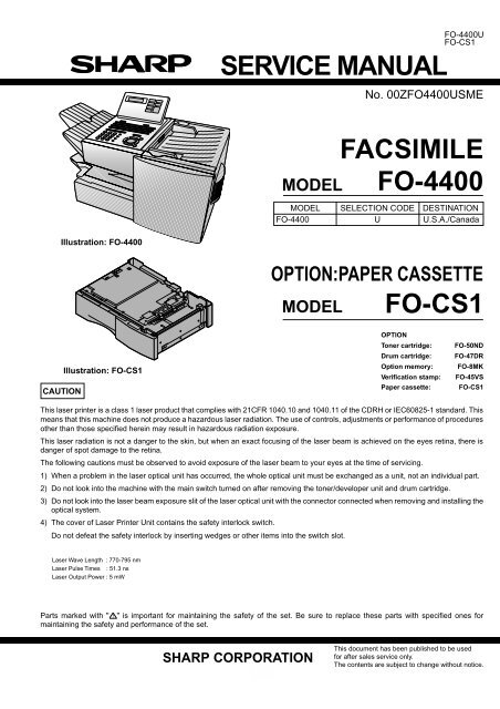
Illustration: <strong>FO</strong>-<strong>4400</strong><br />
CAUTION<br />
Illustration: <strong>FO</strong>-<strong>CS1</strong><br />
Laser Wave Length : 770-795 nm<br />
Laser Pulse Times : 51.3 ns<br />
Laser Output Power : 5 mW<br />
<strong>SERVICE</strong> <strong>MANUAL</strong><br />
1 - 1<br />
<strong>FO</strong>-<strong>4400</strong>U<br />
<strong>FO</strong>-<strong>CS1</strong><br />
No. 00Z<strong>FO</strong><strong>4400</strong>USME<br />
This laser printer is a class 1 laser product that complies with 21CFR 1040.10 and 1040.11 of the CDRH or IEC60825-1 standard. This<br />
means that this machine does not produce a hazardous laser radiation. The use of controls, adjustments or performance of procedures<br />
other than those specified herein may result in hazardous radiation exposure.<br />
This laser radiation is not a danger to the skin, but when an exact focusing of the laser beam is achieved on the eyes retina, there is<br />
danger of spot damage to the retina.<br />
The following cautions must be observed to avoid exposure of the laser beam to your eyes at the time of servicing.<br />
1) When a problem in the laser optical unit has occurred, the whole optical unit must be exchanged as a unit, not an individual part.<br />
2) Do not look into the machine with the main switch turned on after removing the toner/developer unit and drum cartridge.<br />
3) Do not look into the laser beam exposure slit of the laser optical unit with the connector connected when removing and installing the<br />
optical system.<br />
4) The cover of Laser Printer Unit contains the safety interlock switch.<br />
Do not defeat the safety interlock by inserting wedges or other items into the switch slot.<br />
Parts marked with " " is important for maintaining the safety of the set. Be sure to replace these parts with specified ones for<br />
maintaining the safety and performance of the set.<br />
SHARP CORPORATION<br />
<strong>FACSIMILE</strong><br />
MODEL <strong>FO</strong>-<strong>4400</strong><br />
MODEL SELECTION CODE DESTINATION<br />
<strong>FO</strong>-<strong>4400</strong> U U.S.A./Canada<br />
OPTION:PAPER CASSETTE<br />
MODEL <strong>FO</strong>-<strong>CS1</strong><br />
OPTION<br />
Toner cartridge: <strong>FO</strong>-50ND<br />
Drum cartridge: <strong>FO</strong>-47DR<br />
Option memory: <strong>FO</strong>-8MK<br />
Verification stamp: <strong>FO</strong>-45VS<br />
Paper cassette: <strong>FO</strong>-<strong>CS1</strong><br />
This document has been published to be used<br />
for after sales service only.<br />
The contents are subject to change without notice.
<strong>FO</strong>-<strong>4400</strong>U<br />
<strong>FO</strong>-<strong>CS1</strong><br />
CONTENTS<br />
• CAUTION <strong>FO</strong>R BATTERY REPLACEMENT<br />
• PRECAUTIONS <strong>FO</strong>R USING LEAD-FREE SOLDER<br />
CHAPTER 1. GENERAL DESCRIPTION<br />
[1] Specifications . . . . . . . . . . . . . . . . . . . . . . . . . . . . . . . . . . . . . . . . . . . . . . . . . . . . . . . . . . . . . . . . . . 1-1<br />
[2] Life of consumable . . . . . . . . . . . . . . . . . . . . . . . . . . . . . . . . . . . . . . . . . . . . . . . . . . . . . . . . . . . . . . 1-1<br />
[3] Operation panel . . . . . . . . . . . . . . . . . . . . . . . . . . . . . . . . . . . . . . . . . . . . . . . . . . . . . . . . . . . . . . . . 1-2<br />
[4] Transmittable documents . . . . . . . . . . . . . . . . . . . . . . . . . . . . . . . . . . . . . . . . . . . . . . . . . . . . . . . . . 1-3<br />
[5] Installation . . . . . . . . . . . . . . . . . . . . . . . . . . . . . . . . . . . . . . . . . . . . . . . . . . . . . . . . . . . . . . . . . . . . 1-4<br />
[6] Quick reference guide . . . . . . . . . . . . . . . . . . . . . . . . . . . . . . . . . . . . . . . . . . . . . . . . . . . . . . . . . . 1-11<br />
CHAPTER 2. ADJUSTMENTS<br />
[1] Adjustments . . . . . . . . . . . . . . . . . . . . . . . . . . . . . . . . . . . . . . . . . . . . . . . . . . . . . . . . . . . . . . . . . . . 2-1<br />
[2] Diagnostics and service soft switches . . . . . . . . . . . . . . . . . . . . . . . . . . . . . . . . . . . . . . . . . . . . . . . 2-2<br />
[3] Troubleshooting . . . . . . . . . . . . . . . . . . . . . . . . . . . . . . . . . . . . . . . . . . . . . . . . . . . . . . . . . . . . . . . 2-35<br />
[4] Error code table . . . . . . . . . . . . . . . . . . . . . . . . . . . . . . . . . . . . . . . . . . . . . . . . . . . . . . . . . . . . . . . 2-36<br />
[5] Overseas communication mode . . . . . . . . . . . . . . . . . . . . . . . . . . . . . . . . . . . . . . . . . . . . . . . . . . . 2-38<br />
[6] Administrator mode in the personal book function . . . . . . . . . . . . . . . . . . . . . . . . . . . . . . . . . . . . . 2-38<br />
CHAPTER 3. MECHANICAL DESCRIPTION<br />
[1] Mechanical description . . . . . . . . . . . . . . . . . . . . . . . . . . . . . . . . . . . . . . . . . . . . . . . . . . . . . . . . . . . 3-1<br />
[2] Printer description . . . . . . . . . . . . . . . . . . . . . . . . . . . . . . . . . . . . . . . . . . . . . . . . . . . . . . . . . . . . . . 3-2<br />
[3] Disassembly and assembly procedures . . . . . . . . . . . . . . . . . . . . . . . . . . . . . . . . . . . . . . . . . . . . . . 3-9<br />
[4] How to install the verification stamp (<strong>FO</strong>-45VS) . . . . . . . . . . . . . . . . . . . . . . . . . . . . . . . . . . . . . . 3-33<br />
CHAPTER 4. DIAGRAMS<br />
[1] Block diagram . . . . . . . . . . . . . . . . . . . . . . . . . . . . . . . . . . . . . . . . . . . . . . . . . . . . . . . . . . . . . . . . . 4-1<br />
[2] Wiring diagram . . . . . . . . . . . . . . . . . . . . . . . . . . . . . . . . . . . . . . . . . . . . . . . . . . . . . . . . . . . . . . . . . 4-2<br />
[3] Point-to-point diagram and connector signal name . . . . . . . . . . . . . . . . . . . . . . . . . . . . . . . . . . . . . 4-3<br />
CHAPTER 5. CIRCUIT DESCRIPTION<br />
[1] Circuit description . . . . . . . . . . . . . . . . . . . . . . . . . . . . . . . . . . . . . . . . . . . . . . . . . . . . . . . . . . . . . . . 5-1<br />
[2] Circuit description of control PWB . . . . . . . . . . . . . . . . . . . . . . . . . . . . . . . . . . . . . . . . . . . . . . . . . . 5-1<br />
[3] Circuit description of CIS unit . . . . . . . . . . . . . . . . . . . . . . . . . . . . . . . . . . . . . . . . . . . . . . . . . . . . . 5-15<br />
[4] Circuit description of LIU PWB . . . . . . . . . . . . . . . . . . . . . . . . . . . . . . . . . . . . . . . . . . . . . . . . . . . . 5-16<br />
[5] Circuit description of operation panel PWB . . . . . . . . . . . . . . . . . . . . . . . . . . . . . . . . . . . . . . . . . . 5-18<br />
[6] Circuit description of power supply PWB . . . . . . . . . . . . . . . . . . . . . . . . . . . . . . . . . . . . . . . . . . . . 5-19<br />
CHAPTER 6. CIRCUIT SCHEMATICS AND PARTS LAYOUT<br />
[1] Control PWB circuit . . . . . . . . . . . . . . . . . . . . . . . . . . . . . . . . . . . . . . . . . . . . . . . . . . . . . . . . . . . . . 6-1<br />
[2] LIU PWB circuit . . . . . . . . . . . . . . . . . . . . . . . . . . . . . . . . . . . . . . . . . . . . . . . . . . . . . . . . . . . . . . . 6-18<br />
[3] Printer PWB circuit . . . . . . . . . . . . . . . . . . . . . . . . . . . . . . . . . . . . . . . . . . . . . . . . . . . . . . . . . . . . . 6-21<br />
[4] Power supply PWB circuit . . . . . . . . . . . . . . . . . . . . . . . . . . . . . . . . . . . . . . . . . . . . . . . . . . . . . . . 6-25<br />
[5] Operation panel PWB circuit . . . . . . . . . . . . . . . . . . . . . . . . . . . . . . . . . . . . . . . . . . . . . . . . . . . . . 6-27<br />
[6] 2nd paper cassette PWB circuit (<strong>FO</strong>-<strong>CS1</strong>) . . . . . . . . . . . . . . . . . . . . . . . . . . . . . . . . . . . . . . . . . . 6-31<br />
CHAPTER 7. OPERATION FLOWCHART<br />
[1] G3 protocol . . . . . . . . . . . . . . . . . . . . . . . . . . . . . . . . . . . . . . . . . . . . . . . . . . . . . . . . . . . . . . . . . . . . 7-1<br />
[2] Super G3 protocol . . . . . . . . . . . . . . . . . . . . . . . . . . . . . . . . . . . . . . . . . . . . . . . . . . . . . . . . . . . . . . 7-2<br />
[3] Power on sequence . . . . . . . . . . . . . . . . . . . . . . . . . . . . . . . . . . . . . . . . . . . . . . . . . . . . . . . . . . . . . 7-3<br />
CHAPTER 8. OTHERS<br />
[1] Service Tools . . . . . . . . . . . . . . . . . . . . . . . . . . . . . . . . . . . . . . . . . . . . . . . . . . . . . . . . . . . . . . . . . . 8-1<br />
[2] Rewriting version up the FLASH ROM . . . . . . . . . . . . . . . . . . . . . . . . . . . . . . . . . . . . . . . . . . . . . . . 8-2<br />
PARTS GUIDE<br />
1 – 2
(Danish) ADVARSEL !<br />
Lithiumbatteri-Eksplosionsfare ved fejlagtig håndtering.<br />
Udskiftning må kun ske med batteri af samme fabrikat og type.<br />
Levér det brugte batteri tilbage til leverandoren.<br />
(English) Caution !<br />
Danger of explosion if battery is incorrectly replaced.<br />
Replace only with the same or equivalent type<br />
recommended by the equipment manufacturer.<br />
Discard used batteries according to manufacturer’s instructions.<br />
(Finnish) VAROITUS<br />
Paristo voi räjähtää, jos se on virheellisesti asennettu.<br />
Vaihda paristo ainoastaan laitevalmistajan suosittelemaan<br />
tyyppiin. Hävitä käytetty paristo valmistajan ohjeiden mukaisesti.<br />
1 - 3<br />
<strong>FO</strong>-<strong>4400</strong>U<br />
<strong>FO</strong>-<strong>CS1</strong><br />
(French) ATTENTION<br />
Il y a danger d’explosion s’ il y a remplacement incorrect<br />
de la batterie. Remplacer uniquement avec une batterie du<br />
même type ou d’un type recommandé par le constructeur.<br />
Mettre au rébut les batteries usagées conformément aux<br />
instructions du fabricant.<br />
(Swedish) VARNING<br />
Explosionsfare vid felaktigt batteribyte.<br />
Använd samma batterityp eller en ekvivalent<br />
typ som rekommenderas av apparattillverkaren.<br />
Kassera använt batteri enligt fabrikantens<br />
instruktion.<br />
(German) Achtung<br />
Explosionsgefahr bei Verwendung inkorrekter Batterien.<br />
Als Ersatzbatterien dürfen nur Batterien vom gleichen Typ oder<br />
vom Hersteller empfohlene Batterien verwendet werden.<br />
Entsorgung der gebrauchten Batterien nur nach den vom<br />
Hersteller angegebenen Anweisungen.<br />
1 Employing lead-free solder<br />
The Power supply PWB of this model employs lead-free solder. This is indicated by the “LF” symbol printed on the PWB<br />
and in the service manual.<br />
The suffix letter indicates the alloy type of the solder.<br />
Example:<br />
2 Using lead-free solder<br />
Indicates lead-free solder of tin, silver and copper.<br />
When repairing a PWB with the “LF” symbol, only lead-free solder should be used. (Using normal tin/lead alloy solder may<br />
result in cold soldered joints and damage to printed patterns.)<br />
As the melting point of lead-free solder is approximately 40ºC higher than tin/lead alloy solder, it is recommended that a<br />
dedicated bit is used, and that the iron temperature is adjusted accordingly.<br />
3 Soldering<br />
CAUTION <strong>FO</strong>R BATTERY REPLACEMENT<br />
PRECAUTIONS <strong>FO</strong>R USING LEAD-FREE SOLDER<br />
As the melting point of lead-free solder (Sn-Ag-Cu) is higher and has poorer wettability (flow), to prevent damage to the land<br />
of the PWB, extreme care should be taken not to leave the bit in contact with the PWB for an extended period of time.<br />
Remove the bit as soon as a good flow is achieved.<br />
The high content of tin in lead free solder will cause premature corrosion of the bit.<br />
To reduce wear on the bit, reduce the temperature or turn off the iron when it is not required.<br />
Leaving different types of solder on the bit will cause contamination of the different alloys, which will alter their<br />
characteristics, making good soldering more difficult.<br />
It will be necessary to clean and replace bits more often when using lead-free solder. To reduce bit wear, care should be<br />
taken to clean the bit thoroughly after each use.
<strong>FO</strong>-<strong>4400</strong>U<br />
<strong>FO</strong>-<strong>CS1</strong><br />
CHAPTER 1. GENERAL DESCRIPTION<br />
[1] Specifications<br />
• GENERAL<br />
Automatic dialing: Conventional Auto Dialing:<br />
Rapid Key Dialing: 59 numbers<br />
Speed Dialing: 75 numbers<br />
Personal Auto Dial Books: 10 books<br />
(59 Rapid Keys, 16 Speed Dial<br />
numbers per book)<br />
Memory size* : 2 MB (approx. 124 pages)<br />
Optional memory: <strong>FO</strong>-8MK (8 MB;<br />
approx. 500 pages)<br />
Modem speed: 33,600 bps (max.) with automatic<br />
fallback to lower speeds<br />
Transmission time* : Approx. 3 seconds<br />
Toner cartridge yield: Initial starter cartridge (included with<br />
(continuous printing, fax machine): Approx. 3000 pages<br />
4% page coverage, Replacement cartridge (<strong>FO</strong>-50ND):<br />
letter paper) Approx. 6000 pages<br />
Drum cartridge yield: Initial starter cartridge (included with<br />
fax machine): 20,000 pages (avg.)<br />
Replacement cartridge (<strong>FO</strong>-47DR):<br />
20,000 pages (avg.)<br />
Resolution: Horizontal:<br />
203 pixels/inch (8 dots/mm)<br />
Vertical:<br />
Standard: 98 lines/inch (3.85 lines/mm)<br />
Fine/Halftone: 196 lines/inch<br />
(7.7 lines/mm)<br />
Super fine: 391 lines/inch (15.4 lines/mm)<br />
Automatic document feeder: Letter paper (20 lb): Max. 50 pages<br />
Legal paper: Max. 20 pages<br />
(Note: 11” x 17” paper must be loaded<br />
one page at a time.)<br />
Paper capacity: 250 sheets (20 lb)<br />
(500-sheet cassette available as option)<br />
Compression scheme: MMR, MR, MH, Sharp (H2)<br />
Halftone (grayscale): 64 levels<br />
Applicable telephone line: Public switched telephone network<br />
Compatibility: ITU-T (CCITT) G3 mode, Super G3<br />
mode<br />
Printing resolution: Horizontal: 406 lines/inch (16 lines/mm)<br />
Vertical: 391 lines/inch (15.4 lines/mm)<br />
Input document size: Automatic feeding:<br />
Width: 5.8 to 10.1” (148 to 256mm)<br />
Length: 5.0 to 14.3” (128 to 364 mm)<br />
Manual feeding:<br />
Width: 5.8 to 11.0” (148 to 279 mm)<br />
Length: 5.0 to 19.0” (128 to 483 mm)<br />
Effective scanning width: 8.2” (208 mm) max.<br />
Effective printing width: 8.0” (203 mm) max.<br />
Reception modes: Auto/Manual<br />
Instascan speed: 1.3 sec/page (letter paper; scan time<br />
only, excludes document feeding time)<br />
Full Dual Access: Yes<br />
Copy function: Single/Multi/Sort (99 copies/page)<br />
Power requirements: 120 V AC, 60 Hz<br />
Operating temperature: 50 - 86°F(10 - 30°C)<br />
Humidity: 20 to 85 % RH<br />
Power consumption: Stand-by: 9 W<br />
Maximum: 760 W<br />
Dimensions: Width: 21.5” (546 mm)<br />
Depth: 16.2” (412 mm)<br />
Height: 13.6” (346 mm)<br />
(Not including paper tray or attachments)<br />
Weight: Approx. 31.3 lbs. (14.2 kg)<br />
(Not including supplies paper tray or<br />
attachments)<br />
* Based on ITU-T Test Chart #1 at standard resolution, excluding time for<br />
protocol signals (i.e., ITU-T phase C time only).<br />
<br />
To avoid problems with supplies, please don’t use supplies from other units. Please use new supplies, when supply changes are required.<br />
[2] Life of consumable<br />
Section Part Estimated Life Replaced by<br />
Toner cartridge Replacement cartridge 6,000 prints User<br />
(<strong>FO</strong>-50ND) (at Letter/4% chart)<br />
Drum cartridge Replacement cartridge 20,000 prints User<br />
(<strong>FO</strong>-47DR) (at Letter/4% chart)<br />
Paper feed Transfer roller (Refer to the P/G No. 10-8)<br />
(0KW4127410302)<br />
50,000 prints Service Engineer<br />
Fuser Fusing unit (Refer to the P/G No. 9-14)<br />
(0KW4127035501)<br />
50,000 prints Service Engineer<br />
Paper transport Paper transfer roller (Refer to the P/G No. 8-6)<br />
(0KW4127300101)<br />
Cleaning as needed ———————<br />
Unit <strong>FO</strong>-<strong>4400</strong> 5 years or 75,000 prints<br />
of early either<br />
———————<br />
1 – 1
[3] Operation panel<br />
1<br />
2<br />
3<br />
4<br />
5<br />
6<br />
7<br />
7<br />
1<br />
PLAIN PAPER LASER <strong>FACSIMILE</strong><br />
Toner Cartridge<br />
Drum Cartridge<br />
Paper Supply<br />
ALARM Guide<br />
HALF TONE<br />
STANDARD<br />
Paper Jam<br />
Paper Size Error<br />
Printer Cover Open<br />
Out Put Tray Error<br />
CONTRAST RESOLUTION<br />
5<br />
01 02 03 04 05 06 07 08 09 10<br />
Q / ! W / " E / # R / $ T / % Y / & U / ' I / ( O / ) P / =<br />
11 12 13 14 15 16 17 18 19 20<br />
SYMBOL A / | S D F G / { H / } J / [ K / ] L / +<br />
21 22 23 24 25 26 27 28 29 30<br />
Caps Lock Z / < X / > C V B N / * M / ? @ .com<br />
31 32 33 34 35 36 37 38 39<br />
SHIFT / ^ / / \ ; / : Space _ - . / , DEL<br />
7 8 9 10 11 12 13 14 15 16<br />
ALARM<br />
TONER<br />
LINE IN USE<br />
40 41 42 43 44 45 46 47 48 49<br />
Q / ! W / " E / # R / $ T / % Y / & U / ' I / ( O / ) P / =<br />
50 51 52 53 54 55 56 57 58 59<br />
SYMBOL A / | S D F G / { H / } J / [ K / ] L / +<br />
PAGE COUNTER CONFIDENTIAL TIMER COVER SHEET LIFE MEM.STATUS REPORT DOCUMENT<br />
Caps Lock Z / < X / > C V B N / * M / ? @ .com<br />
SHIFT / ^ / / \ ; / : Space _ - . / , DEL<br />
JOB STATUS DUPLEX SCAN PRIORITY BROADCAST<br />
GHI<br />
1<br />
PQRS<br />
7<br />
ABC<br />
JKL<br />
4 5<br />
TUV<br />
OPER<br />
8<br />
0<br />
DEF<br />
2 3<br />
MNO<br />
6<br />
WXYZ<br />
9<br />
PERSONAL<br />
BOOK<br />
SPEED DIAL<br />
REDIAL<br />
SPEAKER<br />
FINE<br />
SUPER FINE<br />
6<br />
MENU<br />
UP<br />
2 3 4<br />
17 18 19 20 21 22 23 24 25<br />
Z<br />
START/<br />
ENTER<br />
A<br />
DOWN<br />
COPY/HELP<br />
STOP<br />
26 27 28 29 30 31<br />
Display<br />
This displays messages and prompts to help you operate the machine.<br />
ALARM indicator<br />
This blinks when one of the paper sources is empty or the drum cartridge is<br />
near the end of its life (printing is still possible). This lights steadily when the<br />
drum cartridge has reached the end of its life, all paper sources are empty, the<br />
print compartment cover is open, or a paper jam has occurred (printing is not<br />
possible). A message will appear in the display to indicate the problem.<br />
TONER indicator<br />
This blinks when the toner cartridge nears empty, and lights steadily when the<br />
toner cartridge needs replacement.<br />
LINE IN USE light<br />
This lights when the fax machine is using the telephone line.<br />
CONTRAST key<br />
Press this key to adjust the contrast before sending or copying a document.<br />
RESOLUTION key<br />
Press this key to adjust the resolution before sending or copying a document.<br />
An indicator will light next to the selected setting (HALFTONE, STANDARD,<br />
FINE or SUPER FINE).<br />
Rapid Dial Keys<br />
Press one of these keys to dial a fax number automatically. (Note that you<br />
must attach the Rapid Key labels.) When navigating through the display<br />
menu, a Rapid Key can also be pressed in place of the numeric keys to<br />
enter a two-digit number (for example, you can press Rapid Key 01 to enter<br />
the number “01”).<br />
1 – 2<br />
8<br />
9<br />
10<br />
11<br />
12<br />
13<br />
14<br />
15<br />
16<br />
17<br />
18<br />
19<br />
20<br />
21<br />
22<br />
23<br />
24<br />
25<br />
26<br />
27<br />
28<br />
29<br />
30<br />
31<br />
SYMBOL key<br />
When entering a name, press this key to enter the symbol on a letter key<br />
(the character to the right of the slash). Press the key again to turn off<br />
symbol entry mode.<br />
<strong>FO</strong>-<strong>4400</strong>U<br />
<strong>FO</strong>-<strong>CS1</strong><br />
PAGE COUNTER key<br />
Press this key to include a slash and the total number of pages after each<br />
page number on the pages of a transmitted document.<br />
CONFIDENTIAL key<br />
Press this key to send or print out a confidential document.<br />
TIMER key<br />
Press this key to set an operation to be performed automatically at a later<br />
time.<br />
COVER SHEET key<br />
Press this key to include a cover sheet when sending a fax.<br />
LIFE key<br />
Press this key, followed by 1 , to check the total number of pages printed<br />
by the fax machine.<br />
MEM. STATUS key<br />
Press this key to check the status of fax transmission jobs, copy jobs, and<br />
fax receptions. This key can also be used to cancel a job.<br />
REPORT key<br />
Press this key to print out a report on the most recently completed<br />
transmission or reception.<br />
DOCUMENT key<br />
Press this key to transmit a document directly from the feeder without<br />
reading it into memory.<br />
JOB STATUS key<br />
Two types of information appear in the display: prompts related to<br />
operations you are performing, and information about how the fax machine<br />
is using the telephone line (transmitting, receiving, etc.). Press this key to<br />
change between the two types of information.<br />
DUPLEX SCAN key<br />
Press this key to transmit or copy a two-sided document.<br />
PRIORITY key<br />
Press this key when you need to transmit a document ahead of other<br />
documents waiting in memory for transmission.<br />
BROADCAST key<br />
Press this key to send a fax to a group of receiving fax machines.<br />
PERSONAL BOOK<br />
Press this key to use or store an auto-dial number in a personal book. If<br />
the book has a passcode, enter the passcode; otherwise, select the book<br />
START/<br />
with or and press ENTER .<br />
SPEED DIAL key<br />
Press this key to dial a Speed Dial number.<br />
MENU key<br />
Press this key to select special functions and settings.<br />
UP and DOWN arrow keys<br />
Volume setting: Press these keys to change the speaker volume when the<br />
SPEAKER key has been pressed, or the ringer volume at any other time.<br />
COPY/HELP key<br />
When a document is in the feeder, press this key to make a copy of a<br />
document. At any other time, press this key to print out the Help List, a<br />
quick reference guide to the operation of your fax machine.<br />
Dial keypad (numeric keys)<br />
Use these keys to dial and program fax numbers.<br />
REDIAL key<br />
Press this key to automatically redial the last number dialed.<br />
SPEAKER key<br />
Press this key when transmitting a document by Normal Dialing to listen to<br />
the line and verify the response of the receiving fax machine.<br />
START/ENTER key<br />
Press this key to begin fax transmission when using Speed Dialing, Direct<br />
Keypad Dialing, or Normal Dialing. This key is also used to select settings<br />
and complete entries when storing names and numbers.<br />
Left and right arrow keys<br />
Auto-dial numbers: Press these keys to search for an auto-dial number<br />
when sending a fax.<br />
MENU key settings: Press these keys after pressing the MENU key to<br />
scroll through the MENU key settings.<br />
STOP key<br />
Press this key to cancel an operation before it is completed.
<strong>FO</strong>-<strong>4400</strong>U<br />
<strong>FO</strong>-<strong>CS1</strong><br />
[4] Transmittable documents<br />
1. Document Sizes<br />
Normal size<br />
(Min.)<br />
128 mm<br />
* With special sizes, only one sheet can be fed into the machine at a<br />
time. Insert next page into feeder as current page is being scanned.<br />
2. Paper Thickness & Weight<br />
3. Document Types<br />
width 5.8" – 10.1" (148 – 256 mm)<br />
length 5.0" – 14.3" (128 – 364 mm)<br />
(Max.)<br />
148 mm 256 mm<br />
[Normal size]<br />
364 mm<br />
(Max.)<br />
279 mm<br />
[Special size]<br />
Product specifications<br />
483 mm<br />
Indication Lower Limit Upper Limit<br />
Weight Japanese indication 45kg paper 70kg paper<br />
indication Size 4 × 6<br />
Metric system 52g/m2 80g/m2 indication<br />
American indication<br />
LB system indication<br />
14 LB 20 LB<br />
Thickness Metric system 0.06mm 0.1mm<br />
indication indication<br />
Inch system indication 0.0024" 0.0035"<br />
Document Document size (148mm × 128mm) ~<br />
size Range W letter (279mm × 483mm)<br />
A4 (210mm × 297mm)<br />
Letter (216mm × 279mm)<br />
Number of Document size B6 ~ Letter/A4 size 50 sheets<br />
ADF sheets Weight B4 size/Legal 20 sheets<br />
W letter size 1 sheet<br />
90 kg (104g/m2 ) or more<br />
135 kg (157g/m2 Paper Kind<br />
) or less 1 sheet<br />
Paper of fine quality/bond paper/<br />
quality Kent paper<br />
• Normal paper<br />
Documents handwritten in pencil (No. 2 lead or softer), fountain pen,<br />
ball point pen, or felt-tipped pen can be transmitted.<br />
Documents of normal contrast duplicated by a copying machine can<br />
also be transmitted.<br />
• Diazo copy (blueprint)<br />
Diazo copy documents of a normal contrast may be transmitted.<br />
• Carbon copy<br />
A carbon copy may be transmitted if its contrast is normal.<br />
1 – 3<br />
4. Cautions on Transmitting Documents<br />
• Documents written in yellow, greenish yellow, or light blue ink cannot<br />
be transmitted.<br />
• Ink, glue, and correcting fluid on documents must be dry before the<br />
documents can be transmitted.<br />
• All clips, staples and pins must be removed from documents before<br />
transmission.<br />
• Patched (taped) documents should be copied first on a copier and<br />
then the copies used for transmission.<br />
• All documents should be fanned before insertion into the feeder to<br />
prevent possible double feeds.<br />
5. Automatic Document Feeder Capacity<br />
Number of pages that can be placed into the feeder at anytime is as<br />
follows:<br />
Normal size: max. 50 sheets (14 lbs - 20 lbs)<br />
Special size: single sheet only (manual feed)<br />
NOTES: • If you need to send or copy more 50 pages, place the additional<br />
pages and carefully in the feeder just before the<br />
last page is scanned. Do not try to force them in, as this<br />
may cause double-feeding or jamming.<br />
• If your document consists of several large or thick pages<br />
which must be loaded one at a time, insert each page into<br />
the feeder as the previous page is being scanned. Insert<br />
gently to prevent doublefeeding.<br />
6. Readable Width & Length<br />
The readable width and length of a document are slightly smaller than<br />
the actual document size.<br />
Note that characters or graphics outside the effective document scanning<br />
range will not be read.<br />
• Readable width<br />
8.2" (208 mm) max.<br />
Readable width<br />
• Readable length<br />
This is the length of the document sent minus 0.16" (4 mm) from the top<br />
and bottom edges.<br />
0.16"(4mm)<br />
Readable length<br />
0.16"(4mm)
[5] Installation<br />
1. Site selection<br />
Take the following points into consideration when selecting a site for this<br />
model.<br />
ENVIRONMENT<br />
• The machine must be installed on a level surface.<br />
• Keep the machine away from air conditioners, heaters, direct sunlight,<br />
and dust.<br />
• Provide easy access to the front, back, and sides of the machine. In<br />
particular, keep the area in front of the machine clear, or the original<br />
document may jam as it comes out after scanning.<br />
• The temperature should be between 50° and 86°F (10° and 30°C).<br />
• The humidity should be between 30% and 85% (without condensation).<br />
ELECTRICITY<br />
AC 120 V, 60 Hz, grounded (3-prong) AC outlet is required.<br />
Caution!<br />
• Connection to a power source other than that specified will cause<br />
damage to the equipment and is not covered under the warranty.<br />
• If your area experiences a high incidence of lightning or power surges,<br />
we recommend that you install a surge protector for the power and<br />
telephone lines. Surge protectors can be purchased at most telephone<br />
specialty stores.<br />
TELEPHONE JACK<br />
A standard RC11C telephone jack must be located near the machine.<br />
This is the telephone jack commonly used in most homes and offices.<br />
• Plugging the fax machine into a jack which is not an RC11C jack may<br />
result in damage to the machine or your telephone system. If you do<br />
not know what kind of jack you have, or need to have one installed,<br />
contact the telephone company.<br />
If the machine is moved from a cold to a warm place...<br />
If the machine is moved from a cold to a warm place, it is possible that<br />
the reading glass may fog up, preventing proper scanning of documents<br />
for transmission. To remove the fog, turn on the power and wait approximately<br />
2 hours before using the machine.<br />
2. Assembly and connections<br />
1 Connecting the power cord<br />
Connect the female end of the power cord to the fax machine as<br />
shown. Insert the male end into a 120 V, 60 Hz, grounded (3-prong)<br />
AC outlet.<br />
Important!: The fax machine requires its own dedicated power outlet.<br />
The power outlet must not be shared with any other devices. In particular,<br />
do not use an extension cord to connect multiple devices to the<br />
outlet.<br />
Note: If your area experiences a high incidence of lightning or power<br />
surges, we recommend that you install surge protectors for the power<br />
and telephone lines. Surge protectors can be purchased at most telephone<br />
specialty stores.<br />
Press the power<br />
switch to turn on<br />
the power.<br />
1 – 4<br />
<strong>FO</strong>-<strong>4400</strong>U<br />
<strong>FO</strong>-<strong>CS1</strong><br />
2 Connecting the telephone line cord<br />
Insert one end of the line cord into the jack on the back of the machine<br />
marked TEL. LINE. Insert the other end into a standard (RJ11C)<br />
single-line wall telephone jack.<br />
Note: The fax machine is set for touch-tone dialing. If you are on a pulse<br />
dial (rotary) line, you must set the fax machine for pulse dialing by changing<br />
Option Setting 22.<br />
3 Attaching the ADF exit tray<br />
Insert the protrusion on the right side of the machine into the hole in<br />
the right side of the ADF exit tray 1 , then bend the tray slightly and<br />
insert so that the protrusion on the left side of the machine goes into<br />
the hole on the left side of the ADF exit tray 2 . Pull out the tray<br />
extension 3 .<br />
2<br />
4 Attaching the received document tray<br />
Slide the received document tray into the machine as shown. When<br />
it stops, lift the end slightly and push in so that the tray locks into<br />
place.<br />
Important!: The received document tray must be attached for the fax<br />
machine to operate properly.<br />
5 Verification Stamp option (<strong>FO</strong>-45VS)<br />
Note: This feature is available as an option. Consult your dealer if<br />
you wish to use this feature.<br />
When transmitting a document, you can have the fax machine stamp<br />
each document page as it is scanned. After scanning, you can check<br />
to see if all document have been stamped to verify that no double<br />
feeds occurred. (A double feed occurs when two pages are fed through<br />
the scanner at once, which means that one of the pages is not<br />
scanned.)<br />
To use this function, have your dealer install the Verification Stamp<br />
option, and then set Option Setting 29 to ON.<br />
1<br />
3
<strong>FO</strong>-<strong>4400</strong>U<br />
<strong>FO</strong>-<strong>CS1</strong><br />
3. Installing the printer cartridges<br />
(Toner cartridge: <strong>FO</strong>-50ND)<br />
(Drum cartridge: <strong>FO</strong>-47DR)<br />
Follow the steps below to install or replace the toner and drum cartridges.<br />
• The initial starter toner cartridge included with the fax machine can<br />
print approximately 3000 letter-size pages (4% coverage of each<br />
page; continuous printing).<br />
• The replacement toner cartridge (<strong>FO</strong>-50ND) can print approximately<br />
6000 letter-size pages.<br />
• The drum cartridge (<strong>FO</strong>-47DR) can print approximately 20,000 letter-size<br />
pages.<br />
1 Press the cover release to open the print compartment cover.<br />
• Caution! The fusing unit inside the print compartment becomes<br />
very hot during operation. Be careful not to touch the<br />
inside of the compartment.<br />
2 If you are replacing the toner cartridge, remove the old cartridge and<br />
dispose of it according to local regulations.<br />
Go directly to STEP 6 if you are only replacing the toner cartridge<br />
and not the drum cartridge.<br />
• If you are replacing the drum cartridge but not the toner cartridge,<br />
remove the toner cartridge and place it on a sheet of paper.<br />
To make the cartridge more compact for disposal, press the buttons on<br />
the ends of the handle and fold the handle down.<br />
1 – 5<br />
3 If you are replacing the drum cartridge, remove the old cartridge and<br />
dispose of it according to local regulations.<br />
4 Remove the new drum cartridge from its packaging. Insert the drum<br />
cartridge into the print compartment.<br />
• Caution! Excessive exposure to light will damage the drum<br />
cartridge. Install the cartridge promptly after removing it<br />
from its packaging.<br />
• Make sure the drum cartridge is inserted in as far as it will go.<br />
BLUE<br />
GREEN<br />
5 If you are installing a new toner cartridge, remove the new toner cartridge<br />
from its packaging. Remove the tape from the cartridge and<br />
then open the cartridge handle so that it stands straight up.<br />
6 Shake as indicated by the arrows to distribute the toner evenly within<br />
the cartridge.<br />
• If the toner is still lumpy after shaking, the gears in the cartridge<br />
may make a noticeable sound when the print compartment cover<br />
is closed after installing the cartridge. This is normal and does not<br />
indicate a problem.
7 Hold the toner cartridge by the handle and insert it into the print compartment.<br />
• Make sure the toner cartridge clicks into place.<br />
• The handle can be left standing up.<br />
BLUE<br />
8 Close the print compartment cover.<br />
GREEN<br />
9 Reset the drum counter by pressing LIFE<br />
V (flip up the Rapid Key<br />
overlay), 3 , and START/<br />
ENTER .<br />
• Note: The toner counter automatically resets each time you replace<br />
the toner cartridge. There is normally no need to reset the toner<br />
counter manually. Should you find it necessary to manually reset the<br />
toner counter, press LIFE<br />
V (flip up the Rapid Key overlay), 2 ,<br />
and START/<br />
ENTER .<br />
Note: The print compartment cover may become noticeably warm if a<br />
large number of pages are successively printed. This is normal and does<br />
not indicate a problem in the machine.<br />
F When to replace the toner cartridge<br />
When the toner cartridge nears empty (about 100 pages can still be<br />
printed), the toner cartridge indicator on the operation panel will blink.<br />
When the toner cartridge is empty, the toner cartridge indicator will<br />
light steadily and REPLACE TONER will appear in the display. Printing<br />
will no longer be possible. Use the following replacement toner<br />
cartridge.<br />
Sharp <strong>FO</strong>-50ND toner cartridge<br />
Hint:<br />
When the toner cartridge nears empty, try taking it out of the machine<br />
and shaking it. This may increase the number of pages that<br />
can be printed before the toner runs out.<br />
G When to replace the drum cartridge<br />
When the drum cartridge nears the end of its life, the ALARM indicator<br />
on the operation panel will blink and DRUM LIFE REACHED will<br />
appear in the display. (this message appears when approximately<br />
1000 pages can still be printed). Use the following replacement drum<br />
cartridge.<br />
Sharp <strong>FO</strong>-47DR drum cartridge<br />
1 – 6<br />
4. Loading printing paper<br />
<strong>FO</strong>-<strong>4400</strong>U<br />
<strong>FO</strong>-<strong>CS1</strong><br />
You can load up to 250 sheets of letter or legal paper (max. 20 lbs.) in<br />
the paper tray.<br />
• A paper cassette is available as an option. Up to 500 sheets of letter<br />
or legal paper can be loaded in the paper cassette. To have the cassette<br />
installed, consult your dealer.<br />
Important: Do not use the back side of paper that has already been<br />
printed on.<br />
Note: If you need to add paper to the tray or cassette while paper still<br />
remains, remove the remaining paper and combine it into a single<br />
stack with the new paper.<br />
Loading paper in the paper tray<br />
1 Remove the received document tray.<br />
2 Insert a stack of paper into the tray, print side up.<br />
• Important! The stack of paper must not be higher than the red line<br />
on the paper tray.<br />
Red line<br />
3 Squeeze the paper guide and move it to match the length of the<br />
paper you are loading.<br />
Attach a letter or<br />
legal label here to<br />
indicate the paper size.<br />
4 Replace the received document tray.<br />
• The received document tray must be attached for the fax machine<br />
to operate properly.
<strong>FO</strong>-<strong>4400</strong>U<br />
<strong>FO</strong>-<strong>CS1</strong><br />
Loading paper in the paper cassette (if installed <strong>FO</strong>-<strong>CS1</strong>)<br />
Note: To use A4 paper in the paper cassette, you must have a service<br />
technician adjust the cassette.<br />
1 Grasp the hand-hold on the cassette and pull the cassette out until it<br />
stops.<br />
2 Push the pressure plate down until it locks into position.<br />
3 Squeeze the paper guide and pull up to move it to the appropriate<br />
holes for the length of the paper. Push the guide down into the holes.<br />
2<br />
1<br />
4 Place a stack of paper in the cassette, print side up.<br />
• Make sure the stack of paper is not higher than the two tabs on the<br />
paper guide and the two metal tabs. If it is, remove some of the<br />
paper.<br />
• If you find it difficult to load the paper, remove the cassette from the<br />
machine. (Pull the cassette out as far as it will go, grasp the left<br />
side of the cassette with your left hand, and then lift it up and out<br />
with both hands.)<br />
5 Push the cassette back into the machine, making sure it clicks into<br />
place.<br />
1 – 7<br />
5. Clearing paper jams<br />
Clearing a jammed document<br />
If the original document doesn’t feed properly during transmission or<br />
copying, or REMOVE ORIGINAL(S) appears in the display, fist try pressing<br />
START/<br />
ENTER . If the document doesn’t feed out, open the operation panel<br />
and remove it.<br />
Important: Do not try to remove a document without opening the operation<br />
panel. This may damage the feeder mechanism.<br />
1 Open the operation panel.<br />
• Squeeze the release marked PANEL RELEASE and pull up.<br />
2 Remove the document.<br />
3 Close the operation panel, making sure it clicks into place.
Clearing a jammed printing paper<br />
If the printing paper jams, PAPER JAM will appear in the display. Follow<br />
the steps below to clear the jam.<br />
1 Press the green release and open the print compartment cover.<br />
• Caution! The fusing unit inside the print compartment becomes<br />
very hot during operation. Be careful not to touch the<br />
inside of the compartment.<br />
2 Remove the toner cartridge and place it on a sheet of paper.<br />
3 Remove the drum cartridge.<br />
4 Remove the jammed paper.<br />
• Make sure no torn pieces of paper remain in the print compartment<br />
and rollers.<br />
OR<br />
1 – 8<br />
<strong>FO</strong>-<strong>4400</strong>U<br />
<strong>FO</strong>-<strong>CS1</strong><br />
5 Replace the drum cartridge.<br />
• Make sure the drum cartridge is inserted in as far as it will go.<br />
BLUE<br />
GREEN<br />
6 Replace the toner cartridge and then close the print compartment<br />
cover.<br />
BLUE<br />
GREEN<br />
7 If you have a paper cassette and the display still indicates that paper<br />
is jammed, pull out the cassette and remove the jammed paper.<br />
8 Replace the paper cassette.
<strong>FO</strong>-<strong>4400</strong>U<br />
<strong>FO</strong>-<strong>CS1</strong><br />
6. Installing the paper cassette (<strong>FO</strong>-<strong>CS1</strong>)<br />
Installing the second paper cassette<br />
Important: Be sure to turn off the power and unplug the power cord<br />
before proceeding.<br />
1 Press the cover release to open the print compartment cover.<br />
2 Remove 6 screws from the rear cover.<br />
Remove the small cover on the left side of the rear cover, and then<br />
remove the screw underneath. Remove the rear cover.<br />
3 Remove 2 screws from the right cover of the machine.<br />
From inside the print compartment, push the 3 tabs indicated in the<br />
blowup out. (Note: The blowup shows the inside of the print compartment.)<br />
Insert your left index finger in between the cover and the machine<br />
as shown, and then close the print compartment cover. With<br />
your index finger still inserted, grasp both sides of the cover and pull<br />
it off.<br />
4 Remove the packing material and tape from the paper cassette.<br />
1 – 9<br />
5 Place the machine on top of the cassette.<br />
1. Insert the cable guide into the cut-out in the edge of the metal<br />
plate, and then fold it in half and hook the top and bottom edges<br />
together.<br />
2. Insert the 15pin cable through the ferrite core, and then connect<br />
the cable to the connectors on the machine and the cassette as<br />
shown. Position the ferrite core in the gap between the bottom<br />
left-hand corner of the circuit board and the side of the<br />
compartment. Insert the cable into the cable guide, and then<br />
insert the remainder of the cable into the slot in the cassette<br />
below the cable guide. Tie the wires with the band.<br />
2<br />
6Replace the small cover over the circuit board and secure it with a<br />
10 mm screw.<br />
7 Attach the support plates to the right side of the machine.<br />
1. Remove the indicated screw.(In Step 8 below, replace it in the<br />
same hole.)<br />
2. Mount the large plate, making sure that the guides fit into the holes<br />
as shown.<br />
3. Mount the small plate, making sure that the guides fit into the holes<br />
as shown.<br />
2<br />
1<br />
A<br />
1<br />
3<br />
P
8 Secure the plates with screws as shown. Use 6 mm screws for the<br />
holes marked with “A”, and 10 mm screws for the holds marked with<br />
“”P”. Secure the screws in the order indicated by the numbers.<br />
A3<br />
A3<br />
P3<br />
A2<br />
9 Replace the right side cover on the machine, inserting the tabs into<br />
the holes.<br />
Attach the longer cassette cover to the right side of the cassette,<br />
inserting the tabs into the holes (first top, then bottom).<br />
1<br />
2<br />
A4<br />
P4<br />
A1<br />
A4<br />
A4<br />
F Replace the screws in the side cover on the machine.<br />
Secure the cassette cover with two 10 mm screws.<br />
A<br />
A<br />
P<br />
P<br />
A<br />
A<br />
P<br />
A<br />
A<br />
A<br />
P<br />
1 – 10<br />
<strong>FO</strong>-<strong>4400</strong>U<br />
<strong>FO</strong>-<strong>CS1</strong><br />
G Attach the support plate to the left side of the machine, inserting the<br />
top edges of the plate under the machine housing. Make sure that<br />
the guides fit into the holes as shown.<br />
Secure the plate with screws as shown. Use 6 mm screws for the<br />
holes marked with “A”, and 10 mm screws for the holes marked with<br />
“P”. Secure the screws in the order indicated by the numbers.<br />
(Note that the top hole on the right does not require a screw.)<br />
H Attach the shorter cassette cover to the left side of the cassette, inserting<br />
the tabs into the holes (first top, then bottom).<br />
2<br />
I Secure the cassette cover with two 10 mm screws.<br />
1<br />
P P<br />
J Replace the rear cover (replace the screw under the small cover on<br />
the left side of the rear cover first, and then replace the small cover).
<strong>FO</strong>-<strong>4400</strong>U<br />
<strong>FO</strong>-<strong>CS1</strong><br />
7. Replacing the Verification Stamp (<strong>FO</strong>-45VS)<br />
If you are using the Verification Stamp function, you will need to replace<br />
the ink cartridge in the stamp unit when it runs out of ink (when the<br />
stamped mark on original documents becomes faint). A new ink cartridge<br />
can be obtained from your dealer.<br />
1 Remove the ADF exit tray.<br />
2 Press down on the protruding tab of the green ink cartridge and pull<br />
the cartridge out with your fingers.<br />
3 Insert the new ink cartridge into the machine (make sure that the tab<br />
is facing out).<br />
4 Replace the ADF exit tray.<br />
2<br />
1<br />
3<br />
1 – 11<br />
[6] Quick reference guide<br />
SENDING FAXES<br />
Place your document (up to 50 letter-size pages) face down in the document<br />
feeder.<br />
(Note: For Normal Dialing and Direct Keypad Dialing, you can also load<br />
the document after dialing the number.)<br />
Press RESOLUTION or CONTRAST<br />
if needed.<br />
Normal Dialing<br />
1. Lift extension phone or press SPEAKER<br />
.<br />
2. Dial the fax number (if using an extension phone, dial on the extension<br />
phone keypad).<br />
3. Wait for the reception tone (if a person answers, ask them to press<br />
their Start key).<br />
4. Press START/<br />
ENTER .<br />
Rapid Key Dialing<br />
1. Press the desired Rapid Key.<br />
Speed Dialing<br />
SPEED DIAL<br />
1. Press and enter the desired Speed Dial number (press START/<br />
ENTER<br />
if you entered a 1-digit number).<br />
2. Press START/<br />
ENTER .<br />
Direct Keypad Dialing<br />
1. Dial the fax number.<br />
2. Press START/<br />
ENTER .<br />
BROADCASTING<br />
1. Load the document and press BROADCAST .<br />
2. Dial destination numbers:<br />
Press a Rapid Key.<br />
Press a Group Key.<br />
SPEED DIAL<br />
Press and enter a Speed Dial number (press START/<br />
ENTER to complete<br />
entry if only one digit is entered).<br />
Enter a full number and press START/<br />
ENTER .<br />
3. When finished, press START/<br />
ENTER .<br />
4. Press RESOLUTION or CONTRAST if needed.<br />
5. Press START/<br />
ENTER .<br />
STORING AUTO DIAL NUMBERS<br />
1. Press MENU , 3 , 0 , 1 .<br />
2. Press 1 to store a number.<br />
(Press 2 to clear a number.)<br />
3. To store a Rapid Key number, press the desired Rapid Key.<br />
SPEED DIAL<br />
To store a Speed Dial number, press and enter a number<br />
from 1 to 75 (press START/<br />
ENTER if you entered a 1-digit number).<br />
(If clearing a number, select it as explained above and then perform<br />
Step 7 and 9.)<br />
4. Enter the full fax number.<br />
5. Press START/<br />
ENTER .<br />
6. Enter a name by pressing the letter keys.<br />
7. Press START/<br />
ENTER .<br />
8. Press 1 if this is a Chain Dial number.<br />
Press 2 if this is a regular number.<br />
9. Press STOP<br />
repeatedly to exit.
CHAPTER 2. ADJUSTMENTS<br />
[1] Adjustments<br />
General<br />
Since the following adjustments and settings are provided for this model,<br />
make adjustments and/or setup as necessary.<br />
1. Adjustments<br />
Adjustments of output voltage (FACTORY ONLY)<br />
1. Install the power supply unit in the machine.<br />
2. Set the recording paper and document.<br />
3. When the document is loaded, power is supplied to the output lines.<br />
Confirm that outputs are within the limits below.<br />
Output voltage settings<br />
POWER<br />
SUPPLY<br />
PWB<br />
HIGH VOLTAGE<br />
PWB<br />
CN5<br />
CN1<br />
12 8<br />
Fig. 1<br />
Output Voltage limits Note<br />
1<br />
1<br />
CN1<br />
10<br />
VR51<br />
[DO NOT TOUCH!]<br />
+5V MAIN 4.947V~5.25V CN5 7pin ↔ 8pin<br />
+24V SUB 23.04V~24.96V CN5 1pin ↔ 2pin<br />
Connector<br />
No.<br />
CN4<br />
Pin No. CN1<br />
1 11 +5V<br />
2 10 CH LREM<br />
3 9 T VR<br />
4 8 T MON V<br />
5 7 T MON I<br />
6 6 B VR<br />
7 5 V REM<br />
8 4 C MON<br />
9 3 MG<br />
10 2 +24V<br />
1<br />
CONTROL PWB<br />
CNPRT1<br />
CNPW1<br />
1 12 1 30<br />
1 30<br />
8<br />
10<br />
CN1<br />
CN7<br />
1<br />
CN4<br />
1<br />
PRINTER PWB<br />
Connector CN5<br />
No.<br />
Pin No. CNPW1<br />
1 +24V SUB<br />
2 MG<br />
3 MG<br />
4 MG<br />
5 +24V MAIN<br />
6 +24V MAIN<br />
7 +5V MAIN<br />
8 DG<br />
9 DG<br />
10 DG<br />
11 +5V MAIN<br />
12 +5V MAIN<br />
Connector CN1<br />
No.<br />
Pin No. CN7<br />
1 +24V MAIN<br />
2 MG<br />
3 DG<br />
4 DG<br />
5 +5V MAIN<br />
6 +5V MAIN<br />
7 HEATER ON<br />
8 H-RELAY OFF<br />
2 – 1<br />
2. IC protectors replacement<br />
(step 2) Select "DIAL MODE".<br />
KEY: 2 2<br />
DISPLAY:<br />
22: DIAL DIAL MODE MODE<br />
1=TONE, 2=PULSE<br />
<strong>FO</strong>-<strong>4400</strong>U<br />
<strong>FO</strong>-<strong>CS1</strong><br />
ICPs (IC Protectors) are installed to protect the CIS unit, panel PWB<br />
unit, TX motor drive circuit and verification stamp drive circuit. ICPs protect<br />
various ICs and electronic circuits from an overcurrent condition.<br />
The location of ICPs are shown below:<br />
(1) F1 (ICP-S0.5) F2 (ICP-S1.0) is installed in order to protect IC’s from<br />
an overcurrent generated in the CIS unit. If F1 or F2 are open,<br />
replace it with a new one.<br />
(2) F5 (ICP-S1.0) is installed in order to protect IC’s from an overcurrent<br />
generated in the panel PWB unit. If F5 is open, replace it with a<br />
new one.<br />
(3) F100 (ICP-S1.0) is installed in order to protect IC’s from an<br />
overcurrent generated in the verification stamp drive circuit. If F100<br />
is open, replace it with a new one.<br />
(4) F101 (ICP-S1.8) is installed in order to protect IC’s from an<br />
overcurrent generated in the TX motor drive circuit. If F101 is open,<br />
replace it with a new one.<br />
In addition to the replacement of F1, F2, F5, F100 and F101, the<br />
factor causing F1, F2, F5, F100 and F101 to open must also be<br />
repaired. If not, F1, F2, F5, F100 and F101 will open again.<br />
Replacement parts<br />
ICP-S0.5 (Sharp code: VHViCPS05//-1)<br />
ICP-S1.0 (Sharp code: VHViCPS10//-1)<br />
ICP-S1.8 (Sharp code: VHViCPS18//-1)<br />
3. Settings<br />
(1) Dial mode selector<br />
OPTION SETTING: DIAL MODE (Soft Switch No. SW2 DATA No. 1)<br />
Use this to set the fax machine to the type of telephone line you are on.<br />
• The factory setting is "TONE".<br />
(step 1) Select "OPTIONAL SETTING".<br />
KEY:<br />
DISPLAY:<br />
KEY:<br />
DISPLAY: TONE SELECTED<br />
KEY:<br />
DISPLAY:<br />
KEY:<br />
MENU 4<br />
4:OPTIONAL SETTING<br />
ENTER #(01-36, , )<br />
(step 3) Select, using "1" or "2".<br />
1<br />
2<br />
PULSE SELECTED<br />
(step 4) End, using the "STOP" key.<br />
STOP<br />
CNLIU1<br />
CONTROL PWB<br />
(TOP SIDE)<br />
1<br />
2<br />
CNSP1<br />
1<br />
CNSEN1<br />
F5 F100<br />
8<br />
F101<br />
F2<br />
28 2<br />
F1 CNCIS1 CNPN1<br />
10 1 27 1 2 1 4 1<br />
CNSTP1<br />
CNTXM1<br />
Fig. 2<br />
IC3<br />
F1/F2/F5:Top side<br />
F100/F101:Bottom side<br />
12 1<br />
CNPW1
<strong>FO</strong>-<strong>4400</strong>U<br />
<strong>FO</strong>-<strong>CS1</strong><br />
[2] Diagnostics and service soft switches<br />
1. Operating procedure<br />
Two kinds of diagnoses are supported.<br />
1-1. Fax diagnosis<br />
This diagnosis is concerned with the main body of fax which is used for<br />
production and service support.<br />
Entering the diagnostic mode<br />
Press MENU 9 8 7 , and the following<br />
display will appear.<br />
MENU 9 8 7<br />
A START SOFT SWITCH MODE<br />
B START PRINT AREA<br />
C START ROM & RAM CHECK<br />
D START AUTO FEEDER MODE<br />
E START AGING MODE<br />
F START PANEL CHECK MODE<br />
G START OPTICAL ADJUST MODE<br />
H START PRODUCT CHECK<br />
I START SIGNAL SEND MODE<br />
J START COMM. CHECK MODE<br />
K START MEMORY CLEAR MODE<br />
L START FLASH MEMORY CHECK<br />
M START ALL FAX/TEL. ENTRY MODE<br />
N<br />
START<br />
START<br />
O START CONF. PASSCODE<br />
P START SIGNAL SEND MODE 2<br />
Q<br />
MAIN: TA68<br />
Then press the START key. Select the desired item with the key<br />
and the key or select with the rapid key.<br />
Enter the mode with the<br />
(Diag • specifications)<br />
START key.<br />
START<br />
TA68<br />
DEPT. PASSCODE<br />
MEMORY SET MODE<br />
R START STAMP AGING MODE<br />
S START DIAL TEST MODE<br />
T<br />
U<br />
START<br />
START<br />
COPY DIAG MODE<br />
LCD CHECK MODE<br />
V START PERSONAL BOOK LIST<br />
W START NO FUNCTION<br />
X START NO FUNCTION<br />
2 – 2<br />
1-2. Print diagnosis<br />
This diagnosis is concerned with the print which is used for production<br />
and service support.<br />
Entering the diagnostic mode<br />
Press MENU 9 8 6 , and the following<br />
display will appear.<br />
PCU ROM VER.:<br />
Then press the START key. Select the desired item with the<br />
key and the key or select with the rapid key.<br />
Enter the mode with the START key.<br />
(Diag •specifications)<br />
MENU 9 8 6<br />
01 START AREA PRINT MODE 1<br />
02 START CHECK PATTERN 1<br />
03<br />
START<br />
CHECK PATTERN 2<br />
04 START CHECK PATTERN 3<br />
05<br />
06<br />
07<br />
08<br />
START<br />
START<br />
START<br />
START<br />
START<br />
CHECK PATTERN 4<br />
PAPER FEED AGING 1<br />
PAPER FEED AGING 2<br />
BIAS ADJUST MODE2<br />
09 START LIFE SET MODE<br />
10<br />
START<br />
PCU ROM Ver.:<br />
LIFE ALL CLEAR<br />
11 START LIFE ENTRY MODE<br />
12<br />
START<br />
LIFE CLEAR MODE<br />
Memory clear when power is turned on<br />
Pressing the START and STOP keys, turn on the main power, and the<br />
following message will be displayed.<br />
MEMORY CLEAR ?<br />
1 = ALL , 2 = IMAGE , 3 = NO<br />
1 = All the data will be deleted including initially registered data.<br />
2 = Delete the image file to be used in transmission. This will delete all<br />
the data related to communication such as reserved transmission or<br />
intercepting. However, the data initially registered will not be deleted.<br />
3 = Memory will not be cleared and the machine enters stand-by mode.
2. Diagnostic items description<br />
2-1. Fax diagnosis<br />
A) Soft switch mode<br />
In this mode, the soft switch are set and the soft switch list is printed.<br />
Soft switch mode screen<br />
S O F T S W I T C H M O D E<br />
S W 0 1 = 0 0 0 0 0 0 0 0<br />
Switch<br />
No.<br />
1 2 3 4 5 6 7 8 :DATA No.<br />
Data<br />
1 Switch number selection<br />
• Press START key for setting of the next soft switch. If the soft<br />
switch number is the final, pressing START key will exit the soft<br />
switch mode.<br />
• Enter two digits of a soft switch number to set the switch number.<br />
If a switch number of nonexistent soft switch is entered, key error<br />
buzzer sounds to reject the input.<br />
S O F T S W I T C H M O D E<br />
S W 0 1 = 0 0 0 0 0 0 0 0<br />
Cursor<br />
E N T E R L A S T D I G I T<br />
S W 1<br />
1 6<br />
S O F T S W I T C H M O D E<br />
S W 1 6 = 0 0 0 1 0 1 1 0<br />
2 Data number selection<br />
The cursor position shows the data to be set.<br />
Pressing # key or → key moves the cursor to the right. If, however,<br />
the cursor is on data number 8, pressing # key or → key shifts the<br />
cursor to data number 1 of the next switch number. If the switch<br />
number is the final, pressing # key or → key will exit the soft switch<br />
mode.<br />
Pressing key or ← key moves the cursor to the left. If, however,<br />
the cursor is on data number 1, pressing key or ← key shifts the<br />
cursor to data number 1 of the former switch number. If the switch<br />
number is 1, pressing key or ← key will not move the cursor and<br />
the error buzzer will sound.<br />
3 Data setting method<br />
Press the MENU key, and the data at the position of the cursor will be<br />
reversed to 0 when it is 1, or to 1 when it is 0. (If the soft switch can<br />
be changed at the bit (Refer to 6.), the error buzzer will sound with<br />
the process not received.)<br />
4 Outputting method of soft switch list<br />
In the soft switch mode, press the REPORT key, and the soft switch<br />
list will be output.<br />
If the recording paper runs out or is clogged, the key error buzzer will<br />
sound with the process not received.<br />
5 Storage of data<br />
In the following case, the data of the soft switches set will be stored.<br />
• It is shifted to set the next soft switch by pressing the START<br />
switch.<br />
• It is shifted to set the next soft switch with the [#] key.<br />
• It is shifted to set the last soft switch with the [ ] key.<br />
• It is shifted to set another soft switch by inputting two digits as the<br />
switch number. (When 2 digits are completely input.)<br />
• Output of the soft switch list is started.<br />
6 Inhibition of data change<br />
(This is also applicable for the optional setting.)<br />
In the following case, it is inhibited to change the data with the key<br />
error buzzer.<br />
• Switching ON/OFF of ECM during the use of image memory.<br />
• OFF to ON of telephone billing function which is using the image<br />
memory is used (Note: In the existing set, the telephone billing<br />
code function is specified from OFF to ON when the timer system<br />
communication (including the batch communication) is set.)<br />
Here, the memory is usable when the telephone billing code function<br />
is on. It can be set from ON to OFF while the memory is<br />
used. However, if setting is practically changed even once, it can<br />
not be returned from OFF to ON.<br />
2 – 3<br />
<strong>FO</strong>-<strong>4400</strong>U<br />
<strong>FO</strong>-<strong>CS1</strong><br />
• OFF to ON of department control function during use of image<br />
memory.<br />
(Note: In the existing set, the department control function is set<br />
from OFF to ON when the timer communication (including the<br />
batch sending) or the memory hold is set.)<br />
• ON to OFF of continuous serial polling function when the continuous<br />
serial polling is started.<br />
(Note: In the existing set, "ON to OFF of the continuous serial<br />
polling function when the continuous serial polling is registered"<br />
has been applied, but the conditions are now moderated. However,<br />
registration is impossible to the program of the new continuous<br />
serial polling when the continuous serial polling function is<br />
OFF.)<br />
• In addition, change of all soft switches during communication<br />
B) Print area<br />
According to the size of the specified sheet, the effective printing area is<br />
printed.<br />
C) ROM & RAM check<br />
This is an item to check if the loaded memory device acts normally.<br />
• The memory devices shown in the following table are checked.<br />
• In case that an error occurs in the device check, the alarm buzzer<br />
shown in the table sounds.<br />
No. Device checked Number of buzzer sound Remarks<br />
1 ROM (PROGRAM FLASH) 1 time :<br />
2 SRAM 2 times 0.5 sec.ON / 0.5 sec.OFF<br />
3 Main D-RAM1 (*1) 3 times :<br />
4 D-RAM2 (*2) 4 times 1.0 sec.ON / 0.5 sec.OFF<br />
5 — —<br />
*1: Work memory (SDRAM 8MB)<br />
*2: Page memory (SDRAM 8MB)<br />
Check device and alarm buzzer<br />
(Example of display) In case that DRAM2 is erroneous.<br />
Display during check Display after check<br />
ROM SRM DRM1 DRM2<br />
ROM SRM DRM1 DRM2<br />
• • • •<br />
P P P E<br />
P=PASS E=ERROR<br />
After the check is complete, the result is outputted.<br />
D) Auto feeder mode<br />
By executing the document insertion and discharge, the automatic feeding<br />
function can be checked. And the document sensor can be checked<br />
as well.<br />
1 Set the document<br />
Before pressing the “START” key, only the document sensor check is<br />
carried out. And as the document sensor is ON, the document size<br />
(A4/B4) and the sensor information (A4/B4/ORG) are displayed.<br />
AUTO FEEDER MODE<br />
( )<br />
After setup of the document<br />
AUTO FEEDER MODE<br />
B4 (A4 B4 ORG)<br />
Only the sensor which is<br />
activated (fallen down) is displayed.)<br />
The paper sheet size (A4/B4) is<br />
displayed.<br />
2 The automatic feeding starts by pressing the “START” key. This mode<br />
ends when the document ends, and the result is printed.
<strong>FO</strong>-<strong>4400</strong>U<br />
<strong>FO</strong>-<strong>CS1</strong><br />
E) Aging mode<br />
This is a mode to execute the copying action and the check pattern<br />
printing action once every 60 minutes and continue the action until 10<br />
sheets are outputted in total.<br />
1 The printing action on the 1st sheet starts by pressing down the<br />
“START” key and entering the mode. When document is set at the<br />
time of the mode start-up the copy action is carried out, and when<br />
the document is not set the “check pattern 1” of the print dialog is<br />
printed.<br />
2 The number of printouts is displayed after printing.<br />
F) Panel check mode<br />
This is to check that each key acts normally and this is displayed on the<br />
LCD according to the key input. And during execution, the document<br />
reading lamp is ON. After inspection start, the LEDs light on sequentially.<br />
At the mode end with the “STOP” key, all of them go OFF. As to the test<br />
result, it is printed out after the mode end.<br />
When the “NUMERIC” key is pressed during the panel check execution,<br />
sending of the DTMF signal corresponding to the key starts,<br />
and when another key is pressed sending of the DTMF signal stops.<br />
• After inputting all the keys, input the “STOP” key at last, and then the<br />
result is displayed.<br />
a) In case that all the keys are pressed.<br />
PANEL CHECK MODE<br />
ALL KEY OK !!<br />
• After the mode end, the test result is printed.<br />
b) In case that there is a key that is not pressed.<br />
PANEL CHECK MODE<br />
KEY ERROR !!<br />
• At the time of NG, the keys that are not pressed are displayed<br />
sequentially, and it becomes the mode to input the key again.<br />
• With the “STOP” key, the re-check is complete.<br />
• After the mode end, the test result is printed.<br />
G) Optical adjust mode<br />
The optical system is adjusted.<br />
• By pressing down the “START” key, the document reading lamp “100%:<br />
ON” is turned ON.<br />
H) Product check<br />
This is a dialog used in the production process and a mode to execute a<br />
specific mode in the series of the flow.<br />
After the mode end, the rest result as to the checked items is printed.<br />
• After moving to the mode, the following actions are sequentially executed.<br />
1 Memory clear (Same as Diagnosis K)<br />
2 Panel check (Same as Diagnosis F)<br />
3 ROM & RAM test check (Same as the Diagnosis C)<br />
4 Test result print<br />
Memory clear printing<br />
Panel check result printing<br />
ROM & RAM test result printing<br />
5 Print area (The specification of each item is the same as the specifi<br />
cation of the simple mode.)<br />
2 – 4<br />
I) Signal send mode<br />
After shift to the mode, press the START key, and the signals will be<br />
transmitted in the following sequence.<br />
It can be used to check the modem and so on.<br />
[ 1] No signals<br />
[ 2] 4800BPS (V. 27ter)<br />
[ 3] 1<strong>4400</strong>BPS (V. 33)<br />
[ 4] 12000BPS (V. 33)<br />
[ 5] 1<strong>4400</strong>BPS (V. 17)<br />
[ 6] 12000BPS (V. 17)<br />
[ 7] 9600BPS (V. 17)<br />
[ 8] 7200BPS (V. 17)<br />
[ 9] 9600BPS (V. 29)<br />
[10] 7200BPS (V. 29)<br />
[11] 4800BPS (V. 29ter)<br />
[12] 2400BPS (V. 29ter)<br />
[13] 300BPS (FLAG)<br />
[14] 2100Hz (CED)<br />
[15] 1100Hz (CNG)<br />
J) Comm. check mode<br />
1 Turn on the Line Monitor. (SW7 No.7, SW37 No.7)<br />
2 Turn off the Cover Sheet Function. (SW2 No.6, SW32 No.6)<br />
3 Set Line Equivalence at 0 km. (SW8 No.1/No.2, SW38 No.1/No.2)<br />
After the check, it is necessary to be sure to return the aforementioned<br />
soft switches into the initial state.<br />
(Clear the memory with the diagnosis.)<br />
K) Memory clear mode<br />
Clear the back-up memory to initialize the soft switches.<br />
The Flash Memory will be initialized. Then, the initialized list be output.<br />
1 Memory clear is executed.<br />
2 The result that says initialized is printed.<br />
NOTE: The life system counter is not cleared.
L) Flash Memory check<br />
This is a mode to check that the flash memory acts normally. The flash<br />
memories shown in the following table are checked.<br />
No. Flash memory Number of buzzer sound Remarks<br />
1 NOR-Flash (Standard) 1 time :<br />
2 NAND-Flash (Standard) 2 times 0.5 sec.ON / 0.5 sec.OFF<br />
3 NAND-Flash (Option) 3 times :<br />
4 — — 1.0 sec.ON / 0.5 sec.OFF<br />
5 — —<br />
• NAND-Flash (optional) is valid only when the optional memory is<br />
mounted.<br />
1 The NOR flash memory test is executed.<br />
NOR FLASH CHECK<br />
S — — — — — — — E<br />
2 The concerned alarm buzzer sounds only when the error occurs.<br />
3 The NAND flash memory test is executed.<br />
NAND FLASH CHECK<br />
S — — — — — — — E<br />
4 The concerned alarm buzzer sounds only when the error occurs.<br />
5 The result is printed.<br />
NOTE:<br />
• During operation of this diagnosis, dual operation is not possible at all.<br />
• If this is excessively repeated, it will shorten the life of the flash memory.<br />
M) All FAX/TEL. entry mode<br />
This is a function to copy the FAX and TEL numbers registered in the<br />
one-touch dialing (RAPID) key [01] to the all one-touch dialing (RAPID)<br />
key and the all abbreviated number (SPEED DIAL) to simplify the FAX<br />
and TEL number registration at the time of aging.<br />
1 Copy the Fax and Tel numbers (including agency) registered in the<br />
one-touch dialing (RAPID) key [01] to all one-touch dialing (RAPID)<br />
key.<br />
2 Copy the FAX and TEL numbers registered in the one-touch dialing<br />
(RAPID) key [01] to the all abbreviated number (SPEED DIAL).<br />
3 In case the chain dial is not set in the one-touch dialing (RAPID) key<br />
[01], register the one-touch dialing (dialing) keys [02] – [59] and all<br />
abbreviated number (SPEED DIAL) to the group number [01].<br />
In case that the chain dial is set, do not create a group, but cancel<br />
only the chain dial setting of the one-touch dialing (RAPID) key [01].<br />
(All except for the one-touch dialing (RAPID) key [01], chain dial is<br />
kept set.)<br />
4 Enter all registered one-touch send (RAPID) keys and speed dial<br />
numbers (SPEED DIAL) on the personal books [01] - [10].<br />
Following this, set the password registration and the password<br />
setting to ON, and set the TTI setting to OFF.<br />
The call-receiver names and book names are specified as follows:<br />
Rapid R XX XX : Rapid key send<br />
SPEED DIAL S XXX XXX : Speed dial number<br />
Personal book BOOK XX XX : Book number<br />
(The letters after 16th letter of the call-receiver’s name registered in the<br />
one-touch dialing [01] are cut off.)<br />
NOTE: Before entering this mode, FAX and TEL numbers must be registered<br />
in the one-touch dialing (RAPID) key [01].<br />
(In case that they are not registered, or a program or a group is<br />
registered, it is not executed.)<br />
N) Dept. passcode<br />
The department passcode list is printed.<br />
O) Conf. passcode<br />
The confidential passcode list is printed.<br />
Differing from printing of one box alone soon after registration, the confidential<br />
passcodes of all boxes are printed.<br />
2 – 5<br />
<strong>FO</strong>-<strong>4400</strong>U<br />
<strong>FO</strong>-<strong>CS1</strong><br />
P) Signal send mode 2<br />
The signals concerned with V.34 & V.8 are checked.<br />
After this mode is activated, press the START key, and the signals will<br />
be sent in the following sequence.<br />
It can be used to check the modem.<br />
[ 1] No signal<br />
[ 2] 33600BPS (V. 34)<br />
[ 3] 31200BPS (V. 34)<br />
[ 4] 28800BPS (V. 34)<br />
[ 5] 26400BPS (V. 34)<br />
[ 6] 24000BPS (V. 34)<br />
[ 7] 21600BPS (V. 34)<br />
[ 8] 19200BPS (V. 34)<br />
[ 9] 16800BPS (V. 34)<br />
[10] 1<strong>4400</strong>BPS (V. 34)<br />
[11] 12000BPS (V. 34)<br />
[12] 9600BPS (V. 34)<br />
[13] 7200BPS (V. 34)<br />
[14] 4800BPS (V. 34)<br />
[15] 2400BPS (V. 34)<br />
[16] 0 - 300BPS (V. 34)<br />
[17] ANSam<br />
Q) Memory set mode<br />
The set and dump list of the memory content is output.<br />
MEMORY SET MODE<br />
AD = 00000000<br />
Cursor<br />
• The address (8 digits (P) generally including the bank information is<br />
input, and the data of 2 digits is continuously input.<br />
Inputting is done in the hexadecimal mode. The ten-key is used for 0<br />
through 9, and the alphabetic keys A (RAPID 01 through 06) are<br />
used for A through F.<br />
MEMORY SET MODE<br />
AD = A02800F6 DATA = 0B<br />
• During data inputting, the address can be moved forward and backward<br />
one byte by one byte with " " and "#". (The address prior to the<br />
address 0 is looped as the maximum address.)<br />
• The Validity of the address is not checked. Accordingly, writing/ reading<br />
operations are possible in the address of the memory not assigned,<br />
the address of ROM and so on.<br />
(However, as practical, writing is not done, and the data content runs<br />
short each reading.)<br />
Though writing is possible in the flash memory, a little time is required.<br />
It is also necessary to take care that the life of the flash memory is<br />
excessively shortened if much data is written in the flash memory.<br />
Since it may run away depending the written content, take minute<br />
care for the writing address.<br />
• When the REPORT key is input, the memory dump list is produced<br />
from the displayed address (here, it is limited at the 16-byte boundary<br />
address (address with end 0) which does not exceed the specified<br />
address and is just in front.). The dump list is output to a maximum<br />
of 99 pages. If any data of one page can be repeatedly developed<br />
and printed, the list is sufficient. But it is not desired that the<br />
content of plural pages are developed in the memory once and are<br />
then printed. If the STOP key is pressed, it will pass to the diagnosis<br />
after the page which is now being printed is completed printed.<br />
If the address exceeds the maximum address, it will return to the<br />
address 0 and printing will be continued.
<strong>FO</strong>-<strong>4400</strong>U<br />
<strong>FO</strong>-<strong>CS1</strong><br />
R) Stamp aging mode<br />
This is a mode to execute the continuous drive aging of the Verification<br />
stamp.<br />
1 Set the document and press down the “START” key and the<br />
continuous drive of the Verification stamp starts.<br />
2 Send the document at the interval of 10 mm and stamp the<br />
Verification stamp continuously. The total number of times of<br />
Verification stamp printing after entering this mode is displayed on<br />
the display.<br />
• Displayed screen during execution<br />
STAMP AGING<br />
TIMES = 13 PAGES = 1<br />
Print total number Page number<br />
of times<br />
3 By pressing down the “STOP” key during the action, or when no<br />
more document is left, the continuous drive of the Verification stamp<br />
stops.<br />
NOTE:<br />
• In case that the document is not set, this cannot be executed.<br />
• The normal action aging that one Verification stamp is pressed on one<br />
sheet of document is executed in the normal copying.<br />
S) Dial test mode<br />
The mode is used to inspect whether dialing is accurate in two kinds of<br />
dial modes . All data which can be dialed in this mode are automatically<br />
called up in both PB mode and DP mode.<br />
[In case that 2 line optional is not mounted.]<br />
1 Turn on CML, and dial the following in the PB mode.<br />
1, 2, 3, 4, 5, 6, 7, 8, 9, , 0, #<br />
2 Dial the following in the DP mode.<br />
1, 5, 9, 0<br />
3 After dialing, turn off CML.<br />
NOTE:<br />
This mode uses the ordinary auto dial. (Accordingly, the signal sending<br />
time and minimum pause are all the same as ordinary.<br />
The measurement result in this mode is completely all the same as in<br />
the ordinary dial mode.)<br />
T) Copy diag mode<br />
This mode is for automatic mode selection of copy to reduce the time for<br />
treatment at the time of production.<br />
1 Set 2 sheets of document. (No problem if there are 2 sheets or<br />
more.)<br />
2 3 sheet continuous copy: 1st sheet in the FINE AUTO<br />
2nd sheet and after that are copied in the<br />
H-TONE DARK.<br />
NOTE:<br />
Input of the image quality and the darkness keys is invalid in this mode.<br />
U) LCD check mode<br />
This is an item to check that the LCD acts normally.<br />
[In case of a 2 lines LCD]<br />
Display “H” to all the digits. (20 letters x 2 lines)<br />
HHHHHHHHHHHHHHHHHHHH<br />
HHHHHHHHHHHHHHHHHHHH<br />
V) Personal book list<br />
The PASSCODE of the personal book 00 to 10 are output.<br />
W) No function<br />
X) No function<br />
2 – 6<br />
2-2. Print diagnosis<br />
Rapid key 01: Area print mode 1<br />
The effective printing area frame is printed in the specified sheet size.<br />
1<br />
2<br />
3<br />
4<br />
5<br />
6<br />
7<br />
8<br />
9<br />
The data pattern used here are as follows and 1 data 30 mm is printed.<br />
1. [Full black pattern]<br />
2. [Intermediate tone 2 pattern]<br />
3. [Intermediate tone 1 pattern]<br />
4. [Mesh point pattern]<br />
5. [Longitudinal strip 2 pattern]<br />
Black 2 dot and white 2 dot are repeated in line.<br />
6. [Lateral strip 2 pattern]<br />
Black 2 line and white 2 line are repeated.<br />
7. [Longitudinal strip 1 pattern]<br />
Black 1 dot and white 1 dot are repeated in line.<br />
8. [Lateral strip 1 pattern]<br />
Black 1 line and white 1 line are repeated.<br />
9. [Full White pattern]<br />
The left pattern is repeated.<br />
The left pattern is repeated.<br />
The left pattern is repeated.
Rapid key 02: Check pattern 1<br />
The lateral stripe 2 pattern is printed on one sheet.<br />
(Black 2 line and white 2 line are repeated.)<br />
Rapid key 03: Check pattern 2<br />
The lateral stripe 2 pattern is printed on multiple pages.<br />
Press the STOP key to end the printing.<br />
Rapid key 04: Check pattern 3<br />
The intermediate tone 1 is printed on one sheet.<br />
Rapid key 05: Check pattern 4<br />
In this mode, 1 sheet is printed as to the square frame pattern for the<br />
skew measurement.<br />
Rapid key 06: Paper feed aging 1<br />
The mode is used for aging related to the printing. In this mode, the<br />
following modes are provided.<br />
1 Blank paper aging mode (ALL WHITE AGING)<br />
2 Whole black print aging mode (ALL BLACK AGING)<br />
3 5% printing aging mode (5% AGING)<br />
4 4% printing aging mode (4% AGING)<br />
5 Outer frame check pattern<br />
6 4% check pattern<br />
After selecting the paper-pass aging mode in the print diagnosis mode,<br />
input the number of each mode above with the ten-key, and the mode<br />
will be executed. The detailed specifications of each mode are described<br />
as follows. Here, the operation in each mode is stopped only when the<br />
STOP key is pressed by the operator or a printing-impossible error occurs.<br />
• Blank paper aging mode<br />
In the mode, printing is continued in the whole white (white paper)<br />
printing pattern until the STOP key is pressed by the operator. (In the<br />
printing area)<br />
• Whole black printing aging mode<br />
In the mode, printing is continued in the whole black (whole black)<br />
printing pattern until the STOP key is pressed by the operator. (In the<br />
printing area)<br />
• 5% aging mode<br />
In this mode, the 5% print pattern is repeatedly printed until the [STOP]<br />
key is pressed by the operator.<br />
• Outer frame pattern aging mode<br />
In this mode, the outer frame check pattern is repeatedly printed until<br />
the [STOP] key is pressed by the operator. For the outer frame, only<br />
the frame showing the printing area is printed.<br />
• 4% chart aging mode<br />
In this mode, the 4% chart is repeatedly printed until the [STOP] key<br />
is pressed by the operator.<br />
Rapid key 07: Paper feed aging 2<br />
This is a mode that is used for aging related to printing, and there are<br />
following modes. And also as to the print interval 5 sec. – 12 hour can<br />
be set.<br />
1 Blank paper aging mode (ALL WHITE AGING)<br />
2 Whole black print aging mode (ALL BLACK AGING)<br />
3 5% printing aging mode (5% AGING)<br />
4 4% printing aging mode (4% AGING)<br />
5 Outer frame check pattern aging mode<br />
6 4% check pattern aging mode<br />
After entering this mode and selecting the paper feeding aging mode,<br />
each mode is executed by inputting the number of the above each mode<br />
with the numeric number keys and then inputting the print interval with<br />
the numeric number keys. Refer to the paper feeding aging mode 1 for<br />
each mode. Each mode stops the action only when the STOP key is<br />
pressed by an operator or when an error for print impossible occurs.<br />
2 – 7<br />
<strong>FO</strong>-<strong>4400</strong>U<br />
<strong>FO</strong>-<strong>CS1</strong><br />
Rapid key 08: Bias adjust mode<br />
The mode is used to adjust the printing density of the printed image.<br />
The image printing density is adjustable in seven steps of 1 to 7.<br />
For details, refer to the following table. (For selection, use the keys 1<br />
through 7.)<br />
Image printing density Thin ← → Thick<br />
Default value<br />
1 2 3 4 5 6 7<br />
Rapid key 09: Life set mode<br />
The mode is used to set the life counter of the printer and the counter of<br />
the auto feeder at desired values. For setting, proceed with the following<br />
procedure.<br />
1 When the life counter setting mode is selected, the following will be<br />
is displayed.<br />
# key<br />
MACH I NE<br />
D R U M<br />
L<br />
L I F E = 0 0 1 2 3 0<br />
L I F E = 0<br />
I F E 1 = 0<br />
L I F E 2 = 0<br />
L I F E 3 = 0<br />
F E E D E R L I F E = 0<br />
0 1 2 3 0<br />
0 1 2 3 0<br />
0 1 2 3 0<br />
0 1 2 3 0<br />
0 1 2 3 0<br />
F E E D E R L I F E = 0<br />
0 1 2 3 0<br />
The cursor blinks at the top data.<br />
Five counters can be selected with the "#" and " " keys.<br />
2 In the state 1, input a desired setting number of 6 digits with the tenkey.<br />
3 After input of 6 digits, shift to another counter with the "#" and " "<br />
keys as necessary. When all necessary counters are completely input,<br />
press the START key.<br />
4 "STORED" will be displayed with the set values stored into the<br />
memory. For checking, retry this mode.<br />
NOTE: The counter shows the operational state of the printer (how many<br />
sheets have been printed since start of use?). The ordinary<br />
memory does not reset the counter. Accordingly, it is necessary<br />
to reset this counter in addition to the ordinary memory clear if<br />
the content in the memory on the control PWB is broken because<br />
of PWB repair, etc. (In the production stage, it is necessary<br />
to execute this in the last process.)<br />
Rapid key 10: Life all clear<br />
The mode is used to clear the life counter of the printer of the counter<br />
of the auto feeder.<br />
NOTE: The counter shows the operational state of the printer (how many<br />
sheets have been printed since start of use?). The ordinary<br />
memory does not reset the counter. Accordingly, it is necessary<br />
to reset this counter in addition to the ordinary memory clear if<br />
the content in the memory on the control PWB is broken because<br />
of PWB repair, etc. (In the production stage, it is necessary<br />
to execute this in the last process.)<br />
key
<strong>FO</strong>-<strong>4400</strong>U<br />
<strong>FO</strong>-<strong>CS1</strong><br />
Rapid key 11: Life entry mode<br />
(For Serviceman temporary counter)<br />
The mode is used to set a desired value for the judgment value (alarm<br />
judgment counter value) of the general purpose life counters 1 through<br />
3 of the printer. If the life of a consumable part (developer, imprinter, etc)<br />
is set, the model which has the error display and RMS function will inform<br />
RMS when the counter reaches the set value. For setting, proceed<br />
with the following procedure.<br />
1 When the life counter setting mode is selected, the following will be<br />
displayed.<br />
L I F E 1 = 0 0 0 0 0 0<br />
# key L I F E 2 = 0 0 0 0 0 0<br />
key<br />
L I F E 3 = 0 0 0 0 0 0<br />
The cursor blinks at the top data.<br />
Three counters can be selected with the "#" and " " keys.<br />
2 In the state 1 , input a desired setting number of 6 digits with the<br />
ten-key.<br />
3 After input of 6 digits, shift to another counter with the "#" and " "<br />
keys as necessary. When all necessary counters are completely input,<br />
press the START key.<br />
4 "STORED" will be displayed with the set values stored into the<br />
memory. For checking, retry this mode.<br />
NOTE: The counter shows the operational state of the printer (how many<br />
sheets have been printed since start of use?). The ordinary<br />
memory does not reset the counter. Accordingly, it is necessary<br />
to reset this counter in addition to the ordinary memory clear if<br />
the content in the memory on the control PWB is broken because<br />
of PWB repair, etc. (In the production stage, it is necessary<br />
to execute this in the last process.)<br />
2 – 8<br />
Rapid key 12: Life clear mode<br />
The mode is used to respectively clear the life counter of the printer and<br />
the counter of the auto feeder. For setting, proceed with the following<br />
procedure.<br />
1 When the life counter clearing mode is selected, the following will be<br />
is displayed.<br />
# key<br />
MACH I NE<br />
D R U M<br />
L<br />
L I F E<br />
L I F E<br />
I F E 1<br />
C L E A R<br />
C L E A R<br />
C L E A R<br />
L I F E 2 C L E A R<br />
L I F E 3 C L E A R<br />
F E E D E R L I F E C L E A R<br />
T O N E R L I F E C L E A R<br />
Seven counters can be selected with the "#" and " " keys.<br />
2 In the state 1, input the DEL key, and the counter will be respectively<br />
cleared.<br />
3 “CLEARED” is displayed and clearing is complete. After ending one<br />
clear, move to another counter to clear with the “#” key, “ ” key, if<br />
necessary. After clearing the necessary counter press down the<br />
“STOP” key.<br />
NOTE: The counter shows the operational state of the printer (how many<br />
sheets have been printed since start of use?). The ordinary<br />
memory does not reset the counter. Accordingly, it is necessary<br />
to reset this counter in addition to the ordinary memory clear if<br />
the content in the memory on the control PWB is broken because<br />
of PWB repair, etc. (In the production stage, it is necessary<br />
to execute this in the last process.)<br />
key
3. How to make soft switch setting<br />
To enter the soft switch mode, make the following key entries in sequence.<br />
Press MENU 9 8 7 START A START<br />
S F T S W 1 = 0 0 0 0 0 0 0 0<br />
S F T S W 1 = 1 0 0 0 0 0 0 0<br />
S F T S W 1 = 1 0 0 0 0 0 0 0<br />
S F T S W 1 = 1 0 0 0 0 0 0 0<br />
S F T S W 1 = 1 0 0 0 0 0 0 0<br />
S F T S W 2 = 0 0 0 0 0 0 0 0<br />
S F T S W 99 = 0 0 0 0 0 0 0 0<br />
The soft switch mode is terminated.<br />
2 – 9<br />
Press MENU key.<br />
Press key.<br />
Press key.<br />
Bit1 - 8 are set.<br />
Press START<br />
key during setting.<br />
Soft SW2 - 99 are set.<br />
<strong>FO</strong>-<strong>4400</strong>U<br />
<strong>FO</strong>-<strong>CS1</strong><br />
To finish the settings halfway between<br />
SW1 and SW99, press the STOP key.<br />
In this case, the setting being done to<br />
the SW No. on display will be nullified<br />
while settings done to the preceding<br />
SW No. remain in effect.
<strong>FO</strong>-<strong>4400</strong>U<br />
<strong>FO</strong>-<strong>CS1</strong><br />
4. Soft switch description<br />
• Soft switch<br />
SW<br />
NO.<br />
SW1<br />
SW2<br />
DATA<br />
NO.<br />
ITEM<br />
Switch setting and function<br />
Initial<br />
setting<br />
Remarks<br />
1 0<br />
1 Recall interval Binary input 8 4 2 1 0 OPTION<br />
2 No. = 1 2 3 4 (Data No.) 1 Set to 1~15<br />
3 EX 0 1 0 1 0<br />
4 eg. Recall interval is set to 5 min. 1<br />
5 Recall times Binary input 8 4 2 1 0 OPTION<br />
6 No. = 5 6 7 8 (Data No.) 0 Set to 0~14<br />
7 EX 0 0 1 0 1<br />
8 eg. Recall times is set to 2 times. 0<br />
1 Dial mode PULSE TONE 0<br />
2 Receive mode AUTO <strong>MANUAL</strong> 1<br />
3 ECM mode Off On 0 OPTION<br />
4 Reserved 0<br />
5 Polling security On Off 1 OPTION<br />
6 Auto cover sheet No Yes 1 OPTION<br />
7 JUNK-FAX function in manual reception Yes No 0<br />
8 JUNK-FAX function Yes No 0 OPTION<br />
1 Number of rings for auto-receive Binary input 8 4 2 1 0 OPTION<br />
2 (0: No ring receive) No. = 1 2 3 4 (Data No.) 0 Set to 0~9<br />
3 EX 0 0 0 1 0<br />
SW3<br />
4<br />
5 Switch to auto-receive from manual receive<br />
eg. Number of rings for auto receive is set to 1 time.<br />
Binary input 8 4 2 1<br />
1<br />
0 OPTION<br />
6 (0: No switch) No. = 5 6 7 8 (Data No.) 0 Set to 0~9<br />
7 EX 0 0 0 0 0<br />
8 eg. Switch to auto receive is set to disable. 0<br />
Communication results printout Printed at Printed at Printed at Not printed Printed OPTION<br />
error only error/timer/ transmis- every time<br />
memory sion mode<br />
only only<br />
1 No. 1 0 0 0 1 1 0<br />
2 No. 2 0 0 1 0 1 0<br />
SW4 3 No. 3 1 0 0 0 0 1<br />
4 Image addition function to the communication On<br />
result table (for memory transmission only)<br />
Off 1 OPTION<br />
5 Reserved 0<br />
SW5<br />
6 TEL billing code function On Off 0 OPTION<br />
7 Billing code position Before After 1 OPTION<br />
8 Multi-TTI feature On Off 0 OPTION<br />
1 Time display format 24 hours 12 hours-AM/PM 0<br />
2 Date display format Month-Day-Year Day-Month-Year 1<br />
3 Header print Off On 0<br />
4 Footer print On Off 0<br />
5 Reserved 0<br />
6 Substitute reception Off On 0<br />
7 Substitute reception conditions Reception disable without TSI Reception enable without TSI 0<br />
8 CSI transmission Off On 0<br />
2 – 10
SW<br />
NO.<br />
SW6<br />
2 JBIG (Joint Bi-level Image Group) option On Off 0<br />
3 MMR On Off 1<br />
4 MR On Off 1<br />
Modem speed V.33 V.17 V. 29 V. 27ter<br />
1<strong>4400</strong> 12000 1<strong>4400</strong> 12000 9600 7200 9600 7200 4800 2400<br />
5 No. 5 0 0 1 1 1 1 0 0 0 0 1<br />
6 No. 6 1 1 0 0 0 0 0 0 0 0 0<br />
7 No. 7 0 1 0 1 0 1 0 1 1 0 0<br />
<strong>FO</strong>-<strong>4400</strong>U<br />
<strong>FO</strong>-<strong>CS1</strong><br />
8 No. 8 0 0 0 0 1 1 1 1 0 0 0<br />
Reception speed fixed NO V. 17- V. 29- V. 27ter-<br />
When 1<strong>4400</strong>bps<br />
1 No. 1 0<br />
1<strong>4400</strong>bps 9600bps<br />
1 0<br />
4800bps<br />
1 0<br />
MODEM used,<br />
setting to<br />
1<strong>4400</strong>bps is<br />
2 No. 2 0 1 1 0 0 ignored.<br />
3 DIS receive acknowledge during Twice Once in NSF reception, twice 0 Effective to<br />
G3 transmission in DIS reception international<br />
SW7 comm.<br />
4 Non-modulated carrier in V.29<br />
transmission mode<br />
On Off 0<br />
5 CNG send when manual TX On Off 1<br />
6 Protocol monitor On Off 0<br />
7 Line monitor On Off 0<br />
8 Reserved 0<br />
Compromised equalizer 0Km 1.8Km 3.6Km 7.2Km Valid when<br />
1 No. 1 0 0 1 1 0 transmitting<br />
2 No. 2 0 1 0 1 0<br />
3 H2 mode No Yes 0<br />
Signal transmission level Binary input 16 8 4 2 1 For For<br />
No. = 4 5 6 7 8 (Data No.) U.S.A Canada<br />
SW8 4 EX 0 1 1 0 1 (For U.S.A.) 0 0<br />
5 EX 0 1 0 0 0 (For Canada) 1 1<br />
6 eg. Signal transmission level is set to -10dBm 1 0<br />
7 0 0<br />
SW9<br />
DATA<br />
NO.<br />
ITEM<br />
1<br />
Switch setting and function<br />
0<br />
Initial<br />
setting<br />
1 JBIG (Joint Bi-level Image Group) On Off 0<br />
8 1 0<br />
CED tone signal interval 75ms 500ms 750ms 1000ms<br />
1 No. 1 0 0 1 1 0<br />
2 No. 2 0 1 0 1 0<br />
3 Equalizer freeze On Off 0<br />
4 Equalizer freeze conditions All 7200bps 0<br />
5 CED detection time 500ms 1000ms 0<br />
Alarm buzzer 3sec 1sec No BEEP No BEEP<br />
6 No. 5 0 0 1 1 0<br />
7 No. 6 0 1 0 1 0<br />
8 Action when RTN received Handle to error Handle to no error 0<br />
2 – 11<br />
Remarks
<strong>FO</strong>-<strong>4400</strong>U<br />
<strong>FO</strong>-<strong>CS1</strong><br />
SW<br />
NO.<br />
DATA<br />
NO.<br />
ITEM<br />
1<br />
Switch setting and function<br />
0<br />
Initial<br />
setting<br />
Remarks<br />
1 Memory retransmission times Binary input 8 4 2 1 1 OPTION<br />
2 No. = 1 2 3 4 (Data No.) 0<br />
3 EX 1 0 1 0 1<br />
SW10<br />
4<br />
5 Memory retransmission interval<br />
eg. Retransmission time set to 10 times.<br />
Binary input 8 4 2 1<br />
0<br />
0 OPTION<br />
6 No. = 5 6 7 8 (Data No.) 0<br />
7 EX 0 0 1 0 1<br />
8 0<br />
1 V.34 mode transmission speed Sending speed = 2400 (bps) x (N+1) 1<br />
2 Example : 1<br />
3 2400 (bps) x 12 = 28800 (bps) 1<br />
SW11<br />
4<br />
5 V.34 mode receiving speed<br />
2400 (bps) is set for N=0. 33600 (bps) is set for N=14.<br />
Receiving speed = 2400 (bps) x (N+1)<br />
0<br />
1<br />
6 Example : 1<br />
7 2400 (bps) x 12 = 28800 (bps) 1<br />
8 2400 (bps) is set for N=0. 33600 (bps) is set for N=14. 0<br />
1 V.34 mode function in case of manual communication On Off 1<br />
2 V.34 mode function On Off 1<br />
3 V.34 control channel communication speed 2400bps 1200bps 0<br />
EOL detection timer 13sec 25sec 5sec 5sec<br />
SW12<br />
4<br />
5<br />
No. 4<br />
No. 5<br />
0<br />
0<br />
0<br />
1<br />
1<br />
0<br />
1<br />
1<br />
0<br />
0<br />
Processing of DIS reception after DIS Command A line is Apply to T.30+α<br />
SW13<br />
SW14<br />
transmission retransmitting cut T.30<br />
6 No. 6 0 0 1 1 0<br />
7 No. 7 0 1 0 1 0<br />
8 The change to DB from DP by Yes No 0<br />
DTMF output level (High) Binary input 16 8 4 2 1 For For<br />
No. = 1 2 3 4 5 (Data No.) n x 0.5dBm U.S.A Canada<br />
1 EX 0 1 1 0 0 (For U.S.A.) 0 0<br />
2 EX 0 1 0 0 0 (For Canada) 1 1<br />
3 eg. Signal transmission level is set to -10dBm 1 0<br />
4 0 0<br />
5 0 0<br />
6 Reserved 0<br />
7 Reserved 0<br />
8 Reserved 0<br />
DTMF output level (Low) Binary input 16 8 4 2 1 For For<br />
No. = 1 2 3 4 5 (Data No.) n x 0.5dBm U.S.A Canada<br />
1 EX 1 0 0 0 0 (For U.S.A.) 1 0<br />
2 EX 0 1 1 0 0 (For Canada) 0 1<br />
3 eg. Signal transmission level is set to -10dBm 0 1<br />
4 0 0<br />
5 0 0<br />
6 Reserved 0<br />
7 Reserved 0<br />
8 Reserved 0<br />
2 – 12
SW<br />
NO.<br />
SW15<br />
SW16<br />
SW17<br />
SW18<br />
SW19<br />
SW20<br />
DATA<br />
NO.<br />
ITEM<br />
1<br />
Switch setting and function<br />
0<br />
Initial<br />
setting<br />
1 Reserved 0<br />
2 Reserved 0<br />
3 Reserved 0<br />
4 Reserved 0<br />
Cl Signal OFF detect enable time (ms) 200 300 350 400 500 700 1200<br />
5 No. 5 0 0 0 0 0 0 0 0<br />
6 No. 6 0 0 0 0 1 1 1 1<br />
7 No. 7 0 0 1 1 0 0 1 0<br />
8 No. 8 0 1 0 1 0 1 0 1<br />
1 Reserved 0<br />
2 Reserved 0<br />
3 Reserved 0<br />
4 Reserved 0<br />
Distinctive ringing OFF STD RING1 RING2 RING3 RING4 RING5<br />
5 No. 5 0 0 1 0 1 0 1 0<br />
6 No. 6 0 0 0 1 1 0 0 0<br />
7 No. 7 0 0 0 0 0 1 1 0<br />
8 No. 8 0 1 0 0 0 0 0 0<br />
1 Reserved 0<br />
2 Reserved 0<br />
3 Reserved 0<br />
4 Reserved 0<br />
5 Reserved 0<br />
6 Reserved 0<br />
7 Reserved 0<br />
8 Reserved 1<br />
1 Reserved 1<br />
2 Reserved 0<br />
3 Reserved 0<br />
4 Reserved 0<br />
5 Reserved 1<br />
6 Reserved 1<br />
7 Reserved 0<br />
8 Reserved 0<br />
1 Reserved 1<br />
2 Reserved 0<br />
3 Reserved 0<br />
4 Reserved 0<br />
5 Reserved 1<br />
6 Reserved 0<br />
7 Reserved 0<br />
8 Reserved 0<br />
1 Reserved 0<br />
2 Reserved 0<br />
3 Reserved 0<br />
4 Reserved 0<br />
5 Reserved 0<br />
6 Reserved 0<br />
7 Reserved 0<br />
8 Reserved 0<br />
2 – 13<br />
<strong>FO</strong>-<strong>4400</strong>U<br />
<strong>FO</strong>-<strong>CS1</strong><br />
Remarks
<strong>FO</strong>-<strong>4400</strong>U<br />
<strong>FO</strong>-<strong>CS1</strong><br />
SW<br />
NO.<br />
2 Reserved 0<br />
3 Reserved 0<br />
Busy tone detection frequency 520~640Hz 300~600Hz 380~500Hz Reserve Reserve<br />
SW21 4 No. 4 0 0 0 0 1 0<br />
SW22<br />
SW23<br />
SW24<br />
SW25<br />
SW26<br />
SW27<br />
DATA<br />
NO.<br />
ITEM<br />
1<br />
Switch setting and function<br />
0<br />
Initial<br />
setting<br />
1 Reserved 0<br />
5 No. 5 0 0 1 1 0 0<br />
6 No. 6 0 1 0 1 0 0<br />
7 Reserved 0<br />
8 Reserved 0<br />
1 Reserved 0<br />
2 Reserved 0<br />
3 Reserved 0<br />
4 Reserved 0<br />
5 Reserved 0<br />
6 Reserved 0<br />
7 Reserved 0<br />
8 Reserved 0<br />
1 Reserved 0<br />
2 Reserved 1<br />
3 Reserved 0<br />
4 Reserved 1<br />
5 Reserved 0<br />
6 Reserved 0<br />
7 Reserved 1<br />
8 Reserved 0<br />
1 Reserved 0<br />
2 Reserved 1<br />
3 Reserved 0<br />
4 Reserved 0<br />
5 Reserved 1<br />
6 Reserved 1<br />
7 Reserved 0<br />
8 Reserved 0<br />
1 Reserved 0<br />
2 Reserved 0<br />
3 Reserved 0<br />
4 Reserved 1<br />
5 Reserved 0<br />
6 Reserved 0<br />
7 Reserved 0<br />
8 Reserved 0<br />
1 Reserved 0<br />
2 Reserved 0<br />
3 Reserved 1<br />
4 Reserved 1<br />
5 Reserved 0<br />
6 Reserved 0<br />
7 Reserved 1<br />
8 Reserved 0<br />
1 Reserved 0<br />
2 Reserved 1<br />
3 Reserved 0<br />
4 Reserved 0<br />
5 Reserved 0<br />
6 Reserved 0<br />
7 Reserved 0<br />
8 Reserved 0<br />
2 – 14<br />
Remarks
SW<br />
NO.<br />
SW28<br />
SW29<br />
SW30<br />
SW31<br />
SW32<br />
SW33<br />
DATA<br />
NO.<br />
ITEM<br />
1<br />
Switch setting and function<br />
0<br />
Initial<br />
setting<br />
1 Reserved 0<br />
2 Reserved 0<br />
3 Reserved 1<br />
4 Reserved 1<br />
5 Reserved 1<br />
6 Reserved 0<br />
7 Reserved 0<br />
8 Reserved 0<br />
1 Reserved 0<br />
2 Reserved 0<br />
3 Reserved 0<br />
4 Reserved 0<br />
5 Reserved 1<br />
6 Reserved 0<br />
7 Reserved 0<br />
8 Reserved 0<br />
1 Reserved 0<br />
2 Reserved 0<br />
3 Reserved 0<br />
For For<br />
U.S.A. Canada<br />
4 Reserved 0 0<br />
5 Reserved 1 1<br />
6 Reserved 1 0<br />
7 Reserved 0 0<br />
8 Reserved 1 0<br />
1 Reserved 0<br />
2 Reserved 0<br />
3 Reserved 0<br />
4 Reserved 0<br />
5 Reserved 0<br />
6 Reserved 0<br />
7 Reserved 0<br />
8 Reserved 0<br />
1 Reserved 1<br />
2 Reserved 0<br />
3 Reserved 1<br />
4 Reserved 0<br />
5 Reserved 0<br />
6 Reserved 0<br />
7 Reserved 1<br />
8 Reserved 0<br />
1 Reserved 1<br />
2 Reserved 1<br />
3 Reserved 1<br />
4 Reserved 0<br />
5 Reserved 1<br />
6 Reserved 1<br />
7 Reserved 1<br />
8 Reserved 0<br />
2 – 15<br />
<strong>FO</strong>-<strong>4400</strong>U<br />
<strong>FO</strong>-<strong>CS1</strong><br />
Remarks
<strong>FO</strong>-<strong>4400</strong>U<br />
<strong>FO</strong>-<strong>CS1</strong><br />
SW<br />
NO.<br />
SW34<br />
SW35<br />
SW36<br />
SW37<br />
SW38<br />
SW39<br />
DATA<br />
NO.<br />
ITEM<br />
1<br />
Switch setting and function<br />
0<br />
Initial<br />
setting<br />
1 Reserved 1<br />
2 Reserved 1<br />
3 Reserved 0<br />
4 Reserved 0<br />
5 Reserved 0<br />
6 Reserved 0<br />
7 Reserved 0<br />
8 Reserved 0<br />
For For<br />
U.S.A. Canada<br />
1 Reserved 0 0<br />
2 Reserved 1 1<br />
3 Reserved 1 0<br />
4 Reserved 0 0<br />
5 Reserved 0 0<br />
6 Reserved 0<br />
7 Reserved 0<br />
8 Reserved 0<br />
For For<br />
U.S.A. Canada<br />
1 Reserved 1 0<br />
2 Reserved 0 1<br />
3 Reserved 0 1<br />
4 Reserved 0 0<br />
5 Reserved 0 0<br />
6 Reserved 0<br />
7 Reserved 0<br />
8 Reserved 0<br />
1 Reserved 0<br />
2 Reserved 0<br />
3 Reserved 0<br />
4 Reserved 0<br />
5 Reserved 0<br />
6 Reserved 1<br />
7 Reserved 0<br />
8 Reserved 1<br />
1 Reserved 0<br />
2 Reserved 0<br />
3 Reserved 0<br />
4 Reserved 0<br />
5 Reserved 0<br />
6 Reserved 0<br />
7 Reserved 0<br />
8 Reserved 0<br />
1 Reserved 0<br />
2 Reserved 0<br />
3 Reserved 0<br />
4 Reserved 0<br />
5 Reserved 0<br />
6 Reserved 0<br />
7 Reserved 0<br />
8 Reserved 1<br />
2 – 16<br />
Remarks
SW<br />
NO.<br />
SW40<br />
SW41<br />
2 Reserved 0<br />
3 Reserved 0<br />
4 Reserved 0<br />
5 Reserved 1<br />
6 Reserved 1<br />
7 Reserved 0<br />
8 Reserved 0<br />
1 Reserved 1<br />
2 Reserved 0<br />
3 Reserved 0<br />
4 Reserved 0<br />
5 Reserved 1<br />
6 Reserved 0<br />
7 Reserved 0<br />
8 Reserved 0<br />
1 Reserved 0<br />
2 Reserved 0<br />
3 Reserved 0<br />
SW42 4 Reserved 0<br />
SW43<br />
SW44<br />
SW45<br />
DATA<br />
NO.<br />
ITEM<br />
1<br />
Switch setting and function<br />
0<br />
Initial<br />
setting<br />
1 Reserved 1<br />
5 Reserved 0<br />
6 Reserved 0<br />
7 Reserved 0<br />
8 Reserved 0<br />
1 Reserved 0<br />
2 Reserved 0<br />
3 Reserved 0<br />
4 Reserved 0<br />
5 Reserved 0<br />
6 Reserved 0<br />
7 Reserved 0<br />
8 Reserved 0<br />
1 Reserved 0<br />
2 Reserved 0<br />
3 Reserved 0<br />
4 Reserved 0<br />
5 Reserved 0<br />
6 Reserved 0<br />
7 Reserved 0<br />
8 Reserved 0<br />
1 Reserved 0<br />
2 Reserved 0<br />
3 Reserved 0<br />
4 Reserved 0<br />
5 Reserved 0<br />
6 Reserved 0<br />
7 Reserved 0<br />
8 Reserved 0<br />
2 – 17<br />
<strong>FO</strong>-<strong>4400</strong>U<br />
<strong>FO</strong>-<strong>CS1</strong><br />
Remarks
<strong>FO</strong>-<strong>4400</strong>U<br />
<strong>FO</strong>-<strong>CS1</strong><br />
SW<br />
NO.<br />
SW46<br />
SW47<br />
SW48<br />
SW49<br />
SW50<br />
SW51<br />
DATA<br />
NO.<br />
ITEM<br />
1<br />
Switch setting and function<br />
0<br />
Initial<br />
setting<br />
Remarks<br />
1 Reserved 0<br />
2 Reserved 0<br />
3 Reserved 0<br />
4 Reserved 0<br />
5 Reserved 0<br />
6 Reserved 0<br />
7 Reserved 0<br />
8 Reserved 0<br />
1 Reserved 0<br />
2 Reserved 0<br />
3 Reserved 0<br />
4 Reserved 0<br />
5 Reserved 0<br />
6 Reserved 0<br />
7 Reserved 0<br />
8 Reserved 0<br />
1 Reserved 0<br />
2 Reserved 0<br />
3 Reserved 0<br />
4 Reserved 0<br />
5 Reserved 0<br />
6 Reserved 0<br />
7 Reserved 0<br />
8 Reserved 0<br />
1 Reserved 0<br />
2 Reserved 0<br />
3 Reserved 0<br />
4 Reserved 0<br />
5 Reserved 0<br />
6 Reserved 0<br />
7 Reserved 0<br />
8 Reserved 0<br />
1 Reserved 0<br />
2 Reserved 0<br />
3 Reserved 0<br />
4 Reserved 0<br />
5 Reserved 0<br />
6 Reserved 0<br />
7 Reserved 0<br />
8 Reserved 0<br />
1 Reserved 0<br />
2 Reserved 0<br />
3 Reserved 0<br />
4 Reserved 0<br />
5 Reserved 0<br />
6 Reserved 0<br />
7 Reserved 0<br />
8 Reserved 0<br />
2 – 18
SW<br />
NO.<br />
SW52<br />
SW53<br />
SW54<br />
SW55<br />
SW56<br />
SW57<br />
<strong>FO</strong>-<strong>4400</strong>U<br />
<strong>FO</strong>-<strong>CS1</strong><br />
DATA<br />
NO.<br />
ITEM<br />
1<br />
Switch setting and function<br />
0<br />
Initial<br />
setting<br />
Remarks<br />
1 Reserved 0<br />
2 Reserved 0<br />
3 Reserved 0<br />
4 Reserved 0<br />
5 Reserved 0<br />
6 Reserved 0<br />
7 Reserved 0<br />
8 Reserved 0<br />
1 Reserved 0<br />
2 Reserved 0<br />
3 Reserved 0<br />
4 Reserved 0<br />
5 Reserved 0<br />
6 Reserved 0<br />
7 Reserved 0<br />
8 Reserved 0<br />
1 Reserved 0<br />
2 Reserved 0<br />
3 Reserved 0<br />
4 Reserved 0<br />
5 Reserved 0<br />
6 Reserved 0<br />
7 Reserved 0<br />
8 Reserved 0<br />
1 Reserved 0<br />
2 Reserved 0<br />
3 Reserved 0<br />
4 Reserved 0<br />
5 Reserved 0<br />
6 Reserved 0<br />
7 Reserved 0<br />
8 Reserved 0<br />
1 Reserved 0<br />
2 Reserved 0<br />
3 Reserved 0<br />
4 Reserved 0<br />
5 Reserved 0<br />
6 Reserved 0<br />
7 Reserved 0<br />
8 Reserved 0<br />
1 Reserved 0<br />
2 Reserved 0<br />
3 Reserved 0<br />
4 Reserved 0<br />
5 Reserved 0<br />
6 Reserved 0<br />
7 Reserved 0<br />
8 Reserved 0<br />
2 – 19
<strong>FO</strong>-<strong>4400</strong>U<br />
<strong>FO</strong>-<strong>CS1</strong><br />
SW<br />
NO.<br />
SW58<br />
SW59<br />
SW60<br />
2 Reserved 0<br />
3 Reserved 0<br />
4 Reserved 0<br />
5 Reserved 0<br />
6 Reserved 0<br />
7 Reserved 0<br />
8 Reserved 0<br />
1 Reserved 0<br />
2 Reserved 0<br />
3 Reserved 0<br />
4 Reserved 0<br />
5 Reserved 0<br />
6 Reserved 0<br />
7 Reserved 0<br />
8 Reserved 0<br />
1 Reserved 0<br />
2 Reserved 0<br />
3 Reserved 0<br />
4 Reserved 0<br />
5 Reserved 0<br />
6 Reserved 0<br />
7 Reserved 0<br />
8 Reserved 0<br />
1 F.A.S.T. (RMS) mode On Off 0<br />
2 Reserved 0<br />
3 Verification stamp Yes No 0<br />
4 Day light saving No Yes 1<br />
SW61 Key buzzer volume Off High Low Low<br />
SW62<br />
SW63<br />
DATA<br />
NO.<br />
ITEM<br />
1<br />
Switch setting and function<br />
0<br />
Initial<br />
setting<br />
1 Reserved 0<br />
5 No. 5 0 0 1 1 1<br />
6 No. 6 0 1 0 1 0<br />
7 Reserved 0<br />
8 Reserved 0<br />
High High Middle Low<br />
1 Speaker volume No. 1 0 0 1 1 1<br />
2 No. 2 0 1 0 1 1<br />
3 Reserved 1<br />
4 Reserved 0<br />
Off High Middle Low<br />
5 Ringer volume No. 5 0 0 1 1 1<br />
6 No. 6 0 1 0 1 1<br />
7 Reserved 0<br />
8 Reserved 0<br />
1 Reserved 0<br />
2 Reserved 1<br />
3 Reserved 0<br />
4 Reserved 0<br />
5 Reserved 1<br />
6 Reserved 0<br />
7 Reserved 1<br />
8 Reserved 0<br />
2 – 20<br />
Remarks
SW<br />
NO.<br />
1 Header registration On Off 0<br />
2 Reserved 0<br />
3 Continuous serial polling On Off 0<br />
<strong>FO</strong>-<strong>4400</strong>U<br />
<strong>FO</strong>-<strong>CS1</strong><br />
Time interval for continuous serial polling OPTION<br />
SW64 0 min. 30 min. 60 min. 120 min. When SW64 -No.3<br />
4 No. 4 0 0 1 1 0 is on, option setting<br />
5 No. 5 0 1 0 1 0 can be set up<br />
6 Reserved 0<br />
7 Reserved 0<br />
8 Quick on line function Yes No 1<br />
Cassette selection Manual Auto-1 Auto-2 Auto-1 OPTION<br />
1 No. 1 0 0 1 1 0<br />
2 No. 2 0 1 0 1 1<br />
The 1st priority cassette None Tray 1st Cass. 2nd Cass. Tray OPTION<br />
SW65<br />
3<br />
4<br />
No. 3<br />
No. 4<br />
0<br />
0<br />
0<br />
0<br />
0<br />
1<br />
0<br />
1<br />
Other<br />
Combination<br />
0<br />
1<br />
It is effective<br />
only when<br />
No.31-1/2 are<br />
5 No. 5 0 1 0 1 0 set up of manual<br />
The 2nd priority cassette None Tray 1st Cass. 2nd Cass. Tray OPTION<br />
6<br />
7<br />
No. 6<br />
No. 7<br />
0<br />
0<br />
0<br />
0<br />
0<br />
1<br />
0<br />
1<br />
Other<br />
Combination<br />
0<br />
1<br />
It is effective<br />
only when<br />
No.31-1/2 are<br />
8 No. 8 0 1 0 1 1 set up of manual<br />
SW66<br />
SW67<br />
SW68<br />
DATA<br />
NO.<br />
ITEM<br />
Switch setting and function<br />
1 0<br />
The 3rd priority cassette None Tray 1st Cass. 2nd Cass. Tray OPTION<br />
1<br />
2<br />
No. 1<br />
No. 2<br />
0<br />
0<br />
0<br />
0<br />
0<br />
1<br />
0<br />
1<br />
Other<br />
Combination<br />
0<br />
0<br />
It is effective<br />
only when<br />
No.31-1/2 are<br />
3 No. 3 0 1 0 1 1 set up of manual<br />
Cassette selection of separate page None Tray 1st Cass. 2nd Cass. OPTION<br />
4 No. 4 0 0 1 1 0<br />
5 No. 5 0 1 0 1 1<br />
6 Reserved 0<br />
7 Reserved 0<br />
8 Reserved 0<br />
Power save mode OFF ON OPTION<br />
1 No.1 0 0 0<br />
2 No.2 0 1 0<br />
Density adjustment of print bias Binary input 4 2 1 set to 1~7.<br />
3 No. = 3 4 5 (Data No.) 1: faint 6: deep 1 set to 0, is<br />
4 EX 1 0 0 0 equal to 4<br />
5 eg. Bias is set to level 4. 0 (100)<br />
Drum life detection No Detection Over only Near and Over Near and Over<br />
6 No. 6 0 0 1 1 1<br />
7 No. 7 0 1 0 1 1<br />
8 Reserved 0<br />
Distinctive ring pattern U.S.A. Canada Australia Hong Kong For For<br />
U.S.A. Canada<br />
1 No. 1 0 0 1 1 0 0<br />
2 No. 2 0 1 0 1 0 1<br />
3 Reserved 0<br />
4 Reserved 1<br />
5 Reserved 0<br />
6 Reserved 0<br />
7 Reserved 1<br />
8 Reserved 0<br />
2 – 21<br />
Initial<br />
setting<br />
Remarks
<strong>FO</strong>-<strong>4400</strong>U<br />
<strong>FO</strong>-<strong>CS1</strong><br />
SW<br />
NO.<br />
SW69<br />
SW70<br />
SW71<br />
SW72<br />
2 Reserved 0<br />
3 Reserved 0<br />
4 Reserved 1<br />
5 Reserved 0<br />
6 Reserved 1<br />
7 Reserved 1<br />
8 Reserved 0<br />
1 Reserved 1<br />
2 Reserved 0<br />
3 Reserved 1<br />
4 Reserved 0<br />
5 Reserved 0<br />
6 Reserved 0<br />
7 Reserved 0<br />
8 Reserved 1<br />
The default resolution for copying Standard Fine S-Fine U-Fine OPTION<br />
1 No. 1 0 0 1 1 0<br />
2 No. 2 0 1 0 1 1<br />
3 Reserved 0<br />
4 Reserved 1<br />
5 Reserved 0<br />
Picture quality priority mode Standard Fine S-Fine U-Fine OPTION<br />
6 No. 6 0 0 1 1 0<br />
7 No. 7 0 1 0 1 0<br />
8 Reserved 0<br />
1 Reserved 1<br />
2 Reserved 0<br />
3 Reserved 1<br />
4 Reserved 0<br />
5 Reserved 0<br />
6 Reserved 0<br />
7 Reserved 0<br />
8 Reserved 0<br />
1 Reserved 0<br />
2 Reserved 0<br />
3 Reserved 0<br />
4 Reserved 0<br />
SW73 5 Reserved 0<br />
SW74<br />
DATA<br />
NO.<br />
ITEM<br />
1<br />
Switch setting and function<br />
0<br />
Initial<br />
setting<br />
1 Reserved 1<br />
Data reduction AUTO 100% The number in ( ) is<br />
6 (Except notation: Setting prohibition) No. 6 0 1 Set up to 100% except the 0 applicable for the<br />
7 No. 7 0 0 notation 0 footer print on. Auto<br />
8 No. 8 0 0 0 is equivalent to 100%.<br />
1 Automatic printing of activity report Yes (When memory full) No (First data is cleared when memory full) 0 OPTION<br />
2 Print out of total time and total number of pages on activity report Off On 0<br />
3 Reserved 0<br />
Remarks<br />
4 Department function On Off 0<br />
5 Department ID digit Binary input 8 4 2 1 0 OPTION<br />
6 No. = 5 6 7 8 (Data No.) 1 set to 3~9<br />
7 EX 0 1 0 0 0<br />
8 eg. Department ID is set to 4 digits 0<br />
2 – 22
SW<br />
NO.<br />
1 Copy protect switch On Off 0<br />
<strong>FO</strong>-<strong>4400</strong>U<br />
<strong>FO</strong>-<strong>CS1</strong><br />
2 Cut-off mode (when copy mode) Continue Cut-off 0 OPTION<br />
3 Scanning ratio in memory input 1 : 1 Reduce 0 Memory scanning<br />
4 Overseas communication mode selection function Yes No 0<br />
SW75 5 Reserved 0<br />
SW76<br />
Reduce ratio when copy mode AUTO 100%<br />
6 (Except notation: Setting prohibition) No. 6 0 1 Set up to 100% except the 1<br />
7 No. 7 0 0 notation 0<br />
8 No. 8 0 0 0<br />
1 Reserved 0<br />
2 Reserved 0<br />
Density adjustment (when Fine/STD mode) Normal Faint Deep Deep (when Dark mode)<br />
3 No. 3 0 0 1 1 0<br />
4 No. 4 0 1 0 1 0<br />
Density adjustment (when Half-tone mode) Normal Faint Deep Deep (when Dark mode)<br />
5 No. 5 0 0 1 1 0<br />
6 No. 6 0 1 0 1 0<br />
7 MTF correction in half-tone mode On Off 1<br />
8 MTF intensity in half-tone mode Strong Weak 0<br />
1 Cassette define LTR/A4: Tray A4 LTR 0<br />
2 Cassette define LTR/A4: Upper A4 LTR 0 When W cassette<br />
3 Cassette define LTR/A4: Lower A4 LTR 0 Ignore when W cassette<br />
4 Reserved 1<br />
SW77 5 Reserved 1<br />
SW78<br />
SW79<br />
SW80<br />
DATA<br />
NO.<br />
ITEM<br />
Switch setting and function<br />
1 0<br />
6 Reserved 0<br />
7 Reserved 0<br />
8 Reserved 0<br />
1 Reserved 1<br />
2 Reserved 0<br />
3 Reserved 0<br />
4 Reserved 0<br />
5 Reserved 0<br />
6 Reserved 0<br />
7 Reserved 0<br />
8 Reserved 0<br />
1 Secure billing code Yes No 0<br />
2 Pause with SHIFT key Yes No 0 Only when special<br />
billing code is given.<br />
3 Reserved 0<br />
4 Z key pause time Binary input 16 8 4 2 1 0 Only when the<br />
5 (250ms unit) No. = 4 5 6 7 8 (Data No.) 0 special billing code<br />
6 EX 0 0 0 0 0 0 is given. The<br />
7 eg. Pause time 250ms 0 ordinary pause is<br />
8 Time=(n+1) x 250ms 0 not affected.<br />
1 Separate feature On Off 0<br />
2 Reserved 0<br />
3 Reserved 0<br />
4 Reserved 0<br />
5 Addition of header (Sender information) On Off 1<br />
6 DTMF sending by the panel test On Off 0<br />
7 Power save mode Real time Timer 1<br />
8 Reserved 0<br />
2 – 23<br />
Initial<br />
setting<br />
Remarks
<strong>FO</strong>-<strong>4400</strong>U<br />
<strong>FO</strong>-<strong>CS1</strong><br />
SW<br />
NO.<br />
SW81<br />
SW82<br />
SW83<br />
SW84<br />
SW85<br />
SW86<br />
DATA<br />
NO.<br />
ITEM<br />
Switch setting and function<br />
1 0<br />
1 Reserved 1<br />
2 Reserved 0<br />
3 Reserved 1<br />
4 Reserved 1<br />
5 Reserved 1<br />
6 Reserved 1<br />
7 Reserved 1<br />
8 Reserved 1<br />
1 Reserved 0<br />
2 Reserved 1<br />
3 Reserved 0<br />
4 Reserved 1<br />
5 Reserved 0<br />
6 Reserved 0<br />
7 Reserved 0<br />
8 Reserved 0<br />
1 Reserved 0<br />
2 Reserved 0<br />
3 Reserved 0<br />
4 Reserved 0<br />
5 Reserved 0<br />
6 Reserved 1<br />
7 Reserved 0<br />
8 Reserved 1<br />
1 Reserved 0<br />
2 Reserved 0<br />
3 Reserved 0<br />
4 Reserved 0<br />
5 Reserved 0<br />
6 Reserved 0<br />
7 Reserved 0<br />
8 Reserved 0<br />
1 Reserved 0<br />
2 Reserved 0<br />
3 Reserved 0<br />
4 Reserved 0<br />
5 Reserved 1<br />
6 Reserved 0<br />
7 Reserved 1<br />
8 Reserved 0<br />
1 Reserved 0<br />
2 Reserved 0<br />
3 Reserved 0<br />
4 Reserved 0<br />
5 Reserved 0<br />
6 Reserved 0<br />
7 Reserved 0<br />
8 Reserved 0<br />
2 – 24<br />
Initial<br />
setting<br />
Remarks
SW<br />
NO.<br />
SW87<br />
SW88<br />
SW89<br />
SW90<br />
SW91<br />
SW92<br />
SW93<br />
DATA<br />
NO.<br />
ITEM<br />
1<br />
Switch setting and function<br />
0<br />
Initial<br />
setting<br />
1 Reserved 0<br />
2 Reserved 0<br />
3 Reserved 0<br />
4 Reserved 0<br />
5 Reserved 0<br />
6 Reserved 0<br />
7 Reserved 0<br />
8 Reserved 0<br />
1 Reserved 0<br />
2 Reserved 0<br />
3 Reserved 0<br />
4 Reserved 0<br />
5 Reserved 0<br />
6 Reserved 0<br />
7 Reserved 0<br />
8 Reserved 0<br />
1 Reserved 0<br />
2 Reserved 0<br />
3 Reserved 0<br />
4 Reserved 0<br />
5 Reserved 0<br />
6 Reserved 0<br />
7 Reserved 0<br />
8 Reserved 1<br />
1 Reserved 0<br />
2 Reserved 0<br />
3 Reserved 1<br />
4 Reserved 0<br />
5 Reserved 0<br />
6 Reserved 1<br />
7 Reserved 0<br />
8 Reserved 1<br />
1 Reserved 0<br />
2 Reserved 0<br />
3 Reserved 0<br />
4 Reserved 0<br />
5 Reserved 0<br />
6 Reserved 0<br />
7 Reserved 0<br />
8 Reserved 0<br />
1 Reserved 0<br />
2 Reserved 1<br />
3 Waiting time after dialing 90sec The specification of each country is followed 0<br />
4 Show receiver’s name Yes (Show) No (Hide) 1<br />
5 Reserved 0<br />
6 Reserved 0<br />
7 Reserved 0<br />
8 Reserved 0<br />
1 Reserved 0<br />
2 Reserved 0<br />
3 Reserved 0<br />
4 Reserved 0<br />
5 Reserved 0<br />
6 Reserved 0<br />
7 Reserved 0<br />
8 Reserved 0<br />
2 – 25<br />
<strong>FO</strong>-<strong>4400</strong>U<br />
<strong>FO</strong>-<strong>CS1</strong><br />
Remarks
<strong>FO</strong>-<strong>4400</strong>U<br />
<strong>FO</strong>-<strong>CS1</strong><br />
SW<br />
NO.<br />
SW94<br />
SW95<br />
SW96<br />
SW97<br />
SW98<br />
SW99<br />
DATA<br />
NO.<br />
ITEM<br />
1<br />
Switch setting and function<br />
0<br />
Initial<br />
setting<br />
1 Reserved 0<br />
2 Reserved 0<br />
3 Reserved 0<br />
4 Reserved 0<br />
5 Reserved 0<br />
6 Reserved 0<br />
7 Reserved 0<br />
8 Reserved 0<br />
1 Reserved 0<br />
2 Reserved 0<br />
3 Reserved 0<br />
4 Reserved 0<br />
5 Reserved 1<br />
6 Reserved 1<br />
7 Reserved 0<br />
8 Reserved 1<br />
1 Reserved 0<br />
2 Reserved 0<br />
3 Reserved 0<br />
4 Reserved 0<br />
5 Reserved 0<br />
6 Reserved 0<br />
7 Reserved 0<br />
8 Reserved 0<br />
1 Reserved 0<br />
2 Reserved 0<br />
3 Reserved 0<br />
4 Reserved 0<br />
5 Reserved 0<br />
6 Reserved 0<br />
7 Reserved 0<br />
8 Reserved 0<br />
1 Reserved 0<br />
2 Reserved 0<br />
3 Reserved 0<br />
4 Reserved 0<br />
5 Reserved 0<br />
6 Reserved 0<br />
7 Reserved 0<br />
8 Reserved 0<br />
1 Reserved 0<br />
For For<br />
U.S.A. Canada<br />
2 Reserved 1 0<br />
For For<br />
U.S.A. Canada<br />
3 Reserved 1 0<br />
4 Reserved 0<br />
5 Reserved 0<br />
6 Reserved 0<br />
7 Reserved 1<br />
8 Reserved 1<br />
2 – 26<br />
Remarks
• Soft switch function description<br />
SW1 No. 1 ~ No. 4 Recall interval<br />
Choice is made for a recall interval for speed and rapid dial numbers.<br />
Use a binary number to program this. If set to 0 accidentally, 1 will be<br />
assumed.<br />
SW1 No. 5 ~ No. 8 Recall times<br />
Choice is made as to how many recall times should be made. Use a<br />
binary number to program this.<br />
SW2 No. 1 Dial mode<br />
Switch the type according to the telephone circuit connected to the facsimile.<br />
0: PULSE DIAL<br />
1: TONE DIAL<br />
SW2 No. 2 Receive mode<br />
Auto/manual receiving mode is set.<br />
SW2 No. 3 ECM mode<br />
Used to determine ECM mode function.<br />
SW2 No. 4 Reserved<br />
Set to "0".<br />
SW2 No. 5 Polling security<br />
This switch is employed to enable or disable the polling operation using<br />
the ID code verification function, in order to prevent unauthorized polling<br />
operation.<br />
SW2 No. 6 Auto cover sheet<br />
When "1" (=YES) is selected, the cover sheet is automatically sent after<br />
transmission of the original to notify the receiver of the number of original<br />
sheets transmitted.<br />
SW2 No. 7 JUNK-FAX function in manual reception<br />
It is set whether JUNK-FAX is functioned in the manual receiving mode<br />
or not.<br />
SW2 No. 8 JUNK-FAX function<br />
This function is used to receive data from a specific remote machine<br />
(station registered in entry mode). It is the function that refused a reception<br />
in the case that TSI of remote machine matched with fax number of<br />
the station registered.<br />
0: No<br />
1: Yes<br />
SW3 No. 1 ~ No. 4 Number of rings for auto-receive<br />
(0: No ring receive)<br />
When the machine is set in the auto receive mode, the number of rings<br />
before answering can be selected. It may be set from one to nine rings<br />
using a binary number. If the soft switch was set to 1, a direct connection<br />
is made to the facsimile. If it was set to 0 accidentally, receive ring is set<br />
to 1. If it was above 9, receive rings are set to 9.<br />
SW3 No. 5 ~ No. 8 Switch to auto-receive from manual receive<br />
(0: No switch)<br />
This setting allows machine to switch from manual to Auto Receive mode.<br />
Setting this number to 0 forces machine to stay in Manual receive mode.<br />
Entering the binary number 0 forces the machine to remain in the manual<br />
answer mode. If a number between 1 and 9 is entered, the machine will<br />
go into the answer mode after the given number of rings. However, it can<br />
be used as an ordinary telephone if the handset is taken off the hook<br />
before this programmed number is finished. If entry of a number above 9<br />
by accident, it will be set to 9. In this case, it must be corrected to the<br />
proper number.<br />
2 – 27<br />
<strong>FO</strong>-<strong>4400</strong>U<br />
<strong>FO</strong>-<strong>CS1</strong><br />
SW4 No. 1 ~ No. 3 Communication results printout<br />
It is possible to obtain communication results after each transaction.<br />
Normally, the switch is set (No. 1: 0, No. 2: 0, No. 3: 1) so that the<br />
communication result is produced only a communication error is encountered.<br />
If No. 1 was set to 1, No. 2 was set to 1 and No. 3 was set to<br />
0, the communication result will be produced every time a communication<br />
is done, even if the communication was successful.<br />
If No. 1 was set to 0, No. 2 to 1 and No. 3 to 0, the communication result<br />
will be produced every transmission.<br />
Setting No. 1 to 1 No. 2 to 0 and No. 3 to 0 will disable this function. No<br />
transaction report will be printed.<br />
If No. 1 was set to 0, No. 2 to 0 and No. 3 to 0, the communication result<br />
is produced only after a timer and memory transmission or when a communication<br />
error is encountered.<br />
SW4 No. 4 Image addition function to the communication result<br />
table (for memory transmission only)<br />
Used to set addition of sending image to the communication result table.<br />
SW4 No. 5 Reserved<br />
Set to "0".<br />
SW4 No. 6 TEL billing code function<br />
When set to "1", the TEL billing code function is enabled.<br />
SW4 No. 7 Billing code position<br />
When set to "1", the billing code is delivered before dialing the remote<br />
number. When set to "0", the billing code is delivered after dialing.<br />
SW4 No. 8 Multi-TTI feature<br />
When this switch is set to "1", Multi TTI function is enabled.<br />
SW5 No. 1 Time display format<br />
When this switch is set to "0", time is displayed in 12-hour system.<br />
When set to "1", 24-hour system.<br />
SW5 No. 2 Date display format<br />
Used to select date display/print formats.<br />
0: DAY-Month-Year<br />
1: Month-DAY-Year<br />
SW5 No. 3 Header print<br />
When it is set at 0, sender’s name, sending page number and so on are<br />
automatically printed in the recording paper on the receiving side during<br />
transmission. Thus, the sender can be known on the receiving side.<br />
0: Applied.<br />
1: Not applied.<br />
SW5 No. 4 Footer print<br />
When set to "1", the date of reception, the sender machine No., and the<br />
page No. are automatically recorded at the end of reception.<br />
SW5 No. 5 Reserved<br />
Set to "0".<br />
SW5 No. 6 Substitute reception<br />
Selection of substitute reception in the case of recording paper ex-hausted<br />
or paper jam. If set to "NO", auto receive is disabled even when the<br />
receive memory is ready to receive.<br />
Substitute reception is not performed even during receive operation.<br />
SW5 No. 7 Substitute reception conditions<br />
Selection of substitute reception according to existence of TEL number<br />
from transmitting side. Initial setting allows substitute reception without<br />
CSI. If set to "no", the receiver cannot receive any documents<br />
SW5 No. 8 CSI transmission<br />
CSI signal contains the sender’s phone number registered in the machine.<br />
If this switch is set to "1", no sender’s name will be printed at the<br />
receiving side.<br />
SW6 No. 1 JBIG (Joint Bi-level Image Group)<br />
An image compression encoding method recommended by ITU-T. It realizes<br />
2-second transmission when the power is turned on.<br />
SW6 No. 2 JBIG (Joint Bi-level Image Group) option<br />
An optional function for JBIG.<br />
SW6 No. 3 MMR<br />
MMR (Modified MR) selects presence of the compression function.
<strong>FO</strong>-<strong>4400</strong>U<br />
<strong>FO</strong>-<strong>CS1</strong><br />
SW6 No. 4 MR<br />
MR (Modified READ) selects presence of the compression function.<br />
SW6 No. 5 ~ No. 8 Modem speed<br />
Used to determine the initial modem speed. The default is<br />
1<strong>4400</strong>BPS(V.17). It may be necessary to program it to a slower speed<br />
when frequent line fallback is encountered, in order to save the time<br />
required for the fallback procedure.<br />
SW7 No. 1, No. 2 Reception speed fixed<br />
The transferable speed of modem in the receiving mode is set.<br />
SW7 No. 3 DIS receive acknowledge during G3 transmission<br />
Used to make a choice of whether reception of NSF (DIS) is acknowledged<br />
after receiving two NSFs (DISs) or receiving one NSF (two DISs).<br />
It may be useful for overseas communication to avoid an echo suppression<br />
problem, if set to 1.<br />
SW7 No. 4 Non-modulated carrier in V.29 transmission mode<br />
Though transmission of a non-modulated carrier is not required for transmission<br />
by the V29 modem according to the CCITT Recommendation, it<br />
may be permitted to send a non-modulated carrier before the image<br />
signal to avoid an echo suppression problem. It may be useful for overseas<br />
communication to avoid an echo suppression problem, if set to 1.<br />
SW7 No. 5 CNG send when manual TX<br />
CNG signal sending ON/OFF in case of manual transmission is set.<br />
SW7 No. 6 Protocol monitor<br />
Normally set to "0". If set to "1", communication can be checked, in case<br />
of troubles, without using a G3 tester or other tools.<br />
When communication FSK data transmission or reception is made, the<br />
data is taken into buffer. When communication is finished, the data<br />
analyzed and printed out. When data is received with the line monitor<br />
(SW7-No. 7) set to "1" the reception level is also printed out.<br />
SW7 No. 7 Line monitor<br />
Normally set to "0". If set to "1", the transmission speed and the reception<br />
level are displayed on the LCD. Used for line tests.<br />
SW7 No. 8 Reserved<br />
Set to "0".<br />
SW8 No. 1, No. 2 Compromised equalizer<br />
The specific line equalizer is inserted.<br />
No. 1 No. 2<br />
0 0 The line equalizer built in the modem is turned off.<br />
0 1 Line equalizer corresponding to 1.8 km<br />
1 0 Line equalizer corresponding to 3.6 km<br />
0 1 Line equalizer corresponding to 7.2 km<br />
SW8 No. 3 H2 mode<br />
Used to determine H2 mode (15sec transmission mode). When set to<br />
OFF, H2 mode is inhibited even though the transmitting machine has<br />
H2 mode.<br />
SW8 No. 4 ~ No. 8 Signal transmission level<br />
Used to control the signal transmission level in the range of –0dB to<br />
–31dB.<br />
SW9 No. 1, No. 2 CED tone signal interval<br />
For international communication, the 2100Hz CED tone may act as an<br />
echo suppresser switch, causing a communication problem. Though this<br />
soft switch is normally set to "0", it should be set to "1" so as to change<br />
the time between CED tone and DIS signal from 75ms to 500ms to<br />
eliminate the communication problem caused by echo.<br />
SW9 No. 3 Equalizer freeze<br />
This switch is used to perform reception operation by fixing the equalizer<br />
control of modem for the line which is always in an unfavorable<br />
state and picture cannot be received. Usually, the control is executed<br />
according to the state of line where the equalizer setting is changed<br />
always.<br />
2 – 28<br />
SW9 No. 4 Equalizer freeze conditions<br />
Setting which specifies SW9 No.3 control only in condition of 7200bps<br />
modem speed.<br />
SW9 No. 5 CED detection time<br />
The detection time of the CED signal from the called side in the auto<br />
calling mode is set.<br />
SW9 No. 6, No. 7 Alarm buzzer<br />
The length of the buzzer for normal end of operation is set.<br />
SW9 No. 8 Action when RTN received<br />
The operation is set when the RTN signal is received in the G3 transmission<br />
mode.<br />
SW10 No. 1 ~ No. 4 Memory retransmission times<br />
The number of memory retransmissions is set.<br />
SW10 No. 5 ~ No. 8 Memory retransmission interval<br />
The interval between memory retransmissions is set.<br />
SW11 No. 1 ~ No. 4 V.34 mode transmission speed<br />
Used to determine the initial modem speed when communication method<br />
is V.34 transmission mode.<br />
SW11 No. 5 ~ No. 8 V.34 mode receiving speed<br />
Used to determine the initial modem speed when communication method<br />
is V.34 reception mode.<br />
SW12 No. 1 V.34 mode function in case of manual communication<br />
Used to select whether the V.34 mode is made valid when automatically<br />
transmitting/receiving.<br />
SW12 No. 2 V.34 mode function<br />
Used to select the V.34 mode for communication when set to “1”, communication<br />
method is V.34 mode..<br />
SW12 No. 3 V.34 control channel communication speed<br />
Used to select the control channel communication speed for V.34 mode.<br />
SW12 No. 4, No. 5 EOL detection timer<br />
Used to make a choice of whether to use the 25-second or 13-second<br />
timer for detection of End of line This is effective to override communication<br />
failures with some facsimile models that have longer End of line<br />
detection.<br />
SW12 No. 6, No. 7 Processing of DIS reception after DIS transmission<br />
When receiving , operation in case of DIS reception after DIS transmission<br />
is selected. Retransmitting command: To retransmit DIS in disregard<br />
of DIS reception.<br />
Breaking circuit: To break circuit instantly. (Abnormal finish)<br />
T. 30: To operate in accordance with T.30.<br />
T. 30+α: To operate in accordance with T.30+α. (To operate differently<br />
according to cases.)<br />
SW12 No. 8 The change to DB from DP by<br />
When setting to 1, the mode is changed by pressing the key from the<br />
pulse dial mode to the tone dial mode.<br />
SW13 No. 1 ~ No. 5 DTMF output level (High)<br />
To set the level to output high group DTMF signals. –15 to 0 dBm (0.5<br />
dBm unit)<br />
SW13 No. 6 ~ No. 8 Reserved<br />
Set to "0".<br />
SW14 No. 1 ~ No. 5 DTMF output level (Low)<br />
To set the level to output low group DTMF signals. –15 to 0 dBm (0.5<br />
dBm unit)<br />
SW14 No. 6 ~ No. 8 Reserved<br />
Set to "0".<br />
SW15 No. 1 ~ No. 4 Reserved<br />
Set to "0".<br />
SW15 No. 5 ~ No. 8 Cl signal OFF detect enable time<br />
Used to set the continuous detection time during OFF period of Cl signal.<br />
SW16 No. 1 ~ No. 4 Reserved<br />
Set to "0".
SW16 No. 5 ~ No. 8 Distinctive ringing<br />
When the ringing setting is turned off, all of the CI signal are received.<br />
When any of the standard, and ring patterns 1 through 3 is selected for<br />
the ringing setting, only the selected CI signal is received.<br />
CI signal patterns<br />
The CI signal patterns consists of the standard pattern, and ring patterns<br />
1 through 7. The standard pattern is the conventional one.<br />
STANDARD<br />
RING<br />
PATTERN 1<br />
for USA<br />
RING<br />
PATTERN 2<br />
for USA<br />
RING<br />
PATTERN 3<br />
for USA<br />
RING<br />
PATTERN 4<br />
for USA<br />
RING<br />
PATTERN 1<br />
for CANADA<br />
RING<br />
PATTERN 2<br />
for CANADA<br />
RING<br />
PATTERN 3<br />
for CANADA<br />
1S<br />
0.8S<br />
0.3S<br />
2S<br />
1.5S<br />
1.5S<br />
0.2S 0.2S<br />
0.4S 0.4S 0.8S<br />
1S<br />
0.5S<br />
2S<br />
0.5S<br />
0.5S 0.5S<br />
0.5S<br />
0.8S<br />
0.4S<br />
1S 0.3S<br />
0.2S 0.2S<br />
1S<br />
0.5S<br />
1S<br />
0.5S<br />
1S<br />
4S<br />
2S<br />
3S<br />
0.5S<br />
1S 0.5S<br />
0.5S<br />
1S<br />
0.5S<br />
1S<br />
4S<br />
4S<br />
4S<br />
4S<br />
4S<br />
3S<br />
3.5S<br />
SW17 No. 1 ~ No. 7 Reserved<br />
Set to "0".<br />
SW17 No. 8 Reserved<br />
Set to "1".<br />
SW18 No. 1 Reserved<br />
Set to "1".<br />
SW18 No. 2 ~ No. 4 Reserved<br />
Set to "0".<br />
SW18 No. 5 , No. 6 Reserved<br />
Set to "1".<br />
SW18 No. 7 , No. 8 Reserved<br />
Set to "0".<br />
SW19 No. 1 Reserved<br />
Set to "1".<br />
SW19 No. 2 ~ No. 4 Reserved<br />
Set to "0".<br />
SW19 No. 5 Reserved<br />
Set to "1".<br />
SW19 No. 6 ~ No. 8 Reserved<br />
Set to "0".<br />
SW20 No. 1 ~ No. 8 Reserved<br />
Set to "0".<br />
SW21 No. 1 ~ No. 3 Reserved<br />
Set to "0".<br />
SW21 No. 4 ~ No. 6 Busy tone detection frequency<br />
To select frequency range of signals to be detected as Busy Tone.<br />
3S<br />
3S<br />
2 – 29<br />
SW21 No. 7, No. 8 Reserved<br />
Set to "0".<br />
SW22 No. 1 ~ No. 8 Reserved<br />
Set to "0".<br />
SW23 No. 1 Reserved<br />
Set to "0".<br />
SW23 No. 2 Reserved<br />
Set to "1".<br />
SW23 No. 3 Reserved<br />
Set to "0".<br />
SW23 No. 4 Reserved<br />
Set to "1".<br />
SW23 No. 5, No. 6 Reserved<br />
Set to "0".<br />
SW23 No. 7 Reserved<br />
Set to "1".<br />
SW23 No. 8 Reserved<br />
Set to "0".<br />
SW24 No. 1 Reserved<br />
Set to "0".<br />
SW24 No. 2 Reserved<br />
Set to "1".<br />
SW24 No. 3, No. 4 Reserved<br />
Set to "0".<br />
SW24 No. 5, No. 6 Reserved<br />
Set to "1".<br />
SW24 No. 7, No. 8 Reserved<br />
Set to "0".<br />
SW25 No. 1 ~ No. 3 Reserved<br />
Set to "0".<br />
SW25 No. 4 Reserved<br />
Set to "1".<br />
SW25 No. 5 ~ No. 8 Reserved<br />
Set to "0".<br />
SW26 No. 1, No. 2 Reserved<br />
Set to "0".<br />
SW26 No. 3, No. 4 Reserved<br />
Set to "1".<br />
SW26 No. 5, No. 6 Reserved<br />
Set to "0".<br />
SW26 No. 7 Reserved<br />
Set to "1".<br />
SW26 No. 8 Reserved<br />
Set to "0".<br />
SW27 No. 1 Reserved<br />
Set to "0".<br />
SW27 No. 2 Reserved<br />
Set to "1".<br />
SW27 No. 3 ~ No. 8 Reserved<br />
Set to "0".<br />
SW28 No. 1, No. 2 Reserved<br />
Set to "0".<br />
SW28 No. 3 ~ No. 5 Reserved<br />
Set to "1".<br />
SW28 No. 6 ~ No. 8 Reserved<br />
Set to "0".<br />
SW29 No. 1 ~ No. 4 Reserved<br />
Set to "0".<br />
SW29 No. 5 Reserved<br />
Set to "1".<br />
SW29 No. 6 ~ No. 8 Reserved<br />
Set to "0".<br />
<strong>FO</strong>-<strong>4400</strong>U<br />
<strong>FO</strong>-<strong>CS1</strong>
<strong>FO</strong>-<strong>4400</strong>U<br />
<strong>FO</strong>-<strong>CS1</strong><br />
SW30 No. 1 ~ No. 4 Reserved<br />
Set to "0".<br />
SW30 No. 5 Reserved (For U.S.A.)<br />
Set to "1".<br />
SW30 No. 6 Reserved (For U.S.A.)<br />
Set to "1".<br />
SW30 No. 6 Reserved (For Canada)<br />
Set to "0".<br />
SW30 No. 7 Reserved<br />
Set to "0".<br />
SW30 No. 8 Reserved (For U.S.A.)<br />
Set to "1".<br />
SW30 No. 8 Reserved (For Canada)<br />
Set to "0".<br />
SW31 No. 1 ~ No. 8 Reserved<br />
Set to "0".<br />
SW32 No. 1 Reserved<br />
Set to "1".<br />
SW32 No. 2 Reserved<br />
Set to "0".<br />
SW32 No. 3 Reserved<br />
Set to "1".<br />
SW32 No. 4 ~ No. 6 Reserved<br />
Set to "0".<br />
SW32 No. 7 Reserved<br />
Set to "1".<br />
SW32 No. 8 Reserved<br />
Set to "0".<br />
SW33 No. 1 ~ No. 3 Reserved<br />
Set to "1".<br />
SW33 No. 4 Reserved<br />
Set to "0".<br />
SW33 No. 5 ~ No. 7 Reserved<br />
Set to "1".<br />
SW33 No. 8 Reserved<br />
Set to "0".<br />
SW34 No. 1, No. 2 Reserved<br />
Set to "1".<br />
SW34 No. 3 ~ No. 8 Reserved<br />
Set to "0".<br />
SW35 No. 1 Reserved<br />
Set to "0".<br />
SW35 No. 2 Reserved<br />
Set to "1".<br />
SW35 No. 3 Reserved (For U.S.A.)<br />
Set to "1".<br />
SW35 No. 3 Reserved (For Canada)<br />
Set to "0".<br />
SW35 No. 4 ~ No. 8 Reserved<br />
Set to "0".<br />
SW36 No. 1 Reserved (For U.S.A.)<br />
Set to "1".<br />
SW36 No. 1 Reserved (For Canada)<br />
Set to "0".<br />
SW36 No. 2 Reserved (For U.S.A.)<br />
Set to "0".<br />
SW36 No. 2 Reserved (For Canada)<br />
Set to "1".<br />
2 – 30<br />
SW36 No. 3 Reserved (For U.S.A.)<br />
Set to "0".<br />
SW36 No. 3 Reserved (For Canada)<br />
Set to "1".<br />
SW36 No. 4 ~ No. 8 Reserved<br />
Set to "0".<br />
SW37 No. 1 ~ No. 5 Reserved<br />
Set to "0".<br />
SW37 No. 6 Reserved<br />
Set to "1".<br />
SW37 No. 7 Reserved<br />
Set to "0".<br />
SW37 No. 8 Reserved<br />
Set to "1".<br />
SW37 No. 5 ~ No. 8 CI signal off detect enable time<br />
Used to set the continuous detection time during OFF period of CI signal.<br />
Normally set to 700ms, where the short ring (500ms: OFF period)<br />
cannot be detected. Therefore, selection of 350ms is allowed.<br />
SW38 No. 1 ~ No. 8 Reserved<br />
Set to "0".<br />
SW39 No. 1 ~ No. 7 Reserved<br />
Set to "0".<br />
SW39 No. 8 Reserved<br />
Set to "1".<br />
SW40 No. 1 Reserved<br />
Set to "1".<br />
SW40 No. 2 ~ No. 4 Reserved<br />
Set to "0".<br />
SW40 No. 5, No. 6 Reserved<br />
Set to "1".<br />
SW40 No. 7, No. 8 Reserved<br />
Set to "0".<br />
SW41 No. 1 Reserved<br />
Set to "1".<br />
SW41 No. 2 ~ No. 4 Reserved<br />
Set to "0".<br />
SW41 No. 5 Reserved<br />
Set to "1".<br />
SW41 No. 6 ~ No. 8 Reserved<br />
Set to "0".<br />
SW42 No. 1 ~ No. 8 Reserved<br />
Set to "0".<br />
SW43 No. 1 ~ No. 8 Reserved<br />
Set to "0".<br />
SW44 No. 1 ~ No. 8 Reserved<br />
Set to "0".<br />
SW45 No. 1 ~ No. 8 Reserved<br />
Set to "0".<br />
SW46 No. 1 ~ No. 8 Reserved<br />
Set to "0".<br />
SW47 No. 1 ~ No. 8 Reserved<br />
Set to "0".<br />
SW48 No. 1 ~ No. 8 Reserved<br />
Set to "0".<br />
SW49 No. 1 ~ No. 8 Reserved<br />
Set to "0".<br />
SW50 No. 1 ~ No. 8 Reserved<br />
Set to "0".<br />
SW51 No. 1 ~ No. 8 Reserved<br />
Set to "0".
SW52 No. 1 ~ No. 8 Reserved<br />
Set to "0".<br />
SW53 No. 1 ~ No. 8 Reserved<br />
Set to "0".<br />
SW54 No. 1 ~ No. 8 Reserved<br />
Set to "0".<br />
SW55 No. 1 ~ No. 8 Reserved<br />
Set to "0".<br />
SW56 No. 1 ~ No. 8 Reserved<br />
Set to "0".<br />
SW57 No. 1 ~ No. 8 Reserved<br />
Set to "0".<br />
SW58 No. 1 ~ No. 8 Reserved<br />
Set to "0".<br />
SW59 No. 1 ~ No. 8 Reserved<br />
Set to "0".<br />
SW60 No. 1 ~ No. 8 Reserved<br />
Set to "0".<br />
SW61 No. 1 F.A.S.T. (RMS) mode<br />
Used to determine a function of remote maintenance system (F.A.S.T.).<br />
SW61 No. 2 Reserved<br />
Set to "0".<br />
SW61 No. 3 Verification stamp<br />
End stamp:<br />
It is set whether the red round mark is stamped at the bottom margin of<br />
the document of every page in the memory input mode and document<br />
sending mode or not.<br />
SW61 No. 4 Day light saving<br />
The day light saving function ON/OFF is set.<br />
SW61 No. 5, No. 6 Key buzzer volume<br />
Key buzzer volume:<br />
The sound volume of key inputting buzzer and other buzzers is set.<br />
SW61 No. 7, No. 8 Reserved<br />
Set to "0".<br />
SW62 No. 1, No. 2 Speaker volume<br />
Speaker volume:<br />
The sound volume of the speaker in the on-hook mode is set.<br />
SW62 No. 3 Reserved<br />
Set to "1".<br />
SW62 No. 4 Reserved<br />
Set to "0".<br />
SW62 No. 5, No. 6 Ringer volume<br />
Ringer volume:<br />
The calling sound volume of CI signal receiving is set.<br />
SW62 No. 7, No. 8 Reserved<br />
Set to "0".<br />
SW63 No. 1 Reserved<br />
Set to "0".<br />
SW63 No. 2 Reserved<br />
Set to "1".<br />
SW63 No. 3, No. 4 Reserved<br />
Set to "0".<br />
SW63 No. 5 Reserved<br />
Set to "1".<br />
SW63 No. 6 Reserved<br />
Set to "0".<br />
SW63 No. 7 Reserved<br />
Set to "1".<br />
SW63 No. 8 Reserved<br />
Set to "0".<br />
SW64 No. 1 Header registration<br />
When setting this switch to "1", registering senders is protected.<br />
2 – 31<br />
<strong>FO</strong>-<strong>4400</strong>U<br />
<strong>FO</strong>-<strong>CS1</strong><br />
SW64 No. 2 Reserved<br />
Set to "0".<br />
SW64 No. 3 Continuous serial polling<br />
Turns ON/OFF the continuous polling function.<br />
SW64 No. 4, No. 5 Time interval for continuous serial polling<br />
Used to set the interval time for continuous serial polling. Normally set<br />
to no interval (0 minute).<br />
SW64 No. 6, No. 7 Reserved<br />
Set to "0".<br />
SW64 No. 8 Quick on line function<br />
It is selected whether auto dial call is activated in the memory input<br />
mode when one document is completely read or when all pages are<br />
completely read.<br />
SW65 No. 1, No. 2 Cassette selection<br />
To set selective modes for detail paper cassettes of the printer.<br />
00: Manual<br />
01: Automatic 1<br />
10: Automatic 2<br />
11: Except the above<br />
To select detail paper in the first priority<br />
cassette in accordance with setting<br />
by SW65 3-8 and SW65 1-3. If the detail<br />
paper in the first priority cassette<br />
runs short, the second priority cassette<br />
will be used.<br />
To automatically select detail paper with<br />
optimum size among the first to third<br />
priority cassettes in accordance with<br />
setting by SW65 3-8 and SW65 1-3.<br />
The optimum paper is selected by every<br />
page. If all the cassettes have the same<br />
size paper, paper will be selected according<br />
to the cassette priority.<br />
To automatically select detail paper with<br />
optimum size among the first to third<br />
priority cassettes in accordance with<br />
setting by SW65 3-8 and SW65 1-3. At<br />
the start of printing, the optimum paper<br />
is adopted only for the first page.<br />
Thereafter the same cassette selected<br />
for the first page will be used from the<br />
second page and after. If all the cassettes<br />
have the same size paper, paper<br />
will be selected according to the<br />
cassette priority.<br />
01: the same setting as in the case of<br />
Automatic 1<br />
SW65 No. 3 ~ No. 5 The 1st priority cassette<br />
To select the first priority cassette.<br />
001: 1st paper feeder (MP-TRAY)<br />
010: 2nd paper feeder<br />
011: 3rd paper feeder<br />
Except the above Printing started from the possible paper feeder<br />
SW65 No. 6 ~ No. 8 The 2nd priority cassette<br />
To select the second priority cassette.<br />
000: Not used (To set in case of using only paper<br />
feeder that has been set in the first priority<br />
cassette)<br />
001: 1st paper feeder (MP-TRAY)<br />
010: 2nd paper feeder<br />
011: 3rd paper feeder<br />
Except the above Not used
<strong>FO</strong>-<strong>4400</strong>U<br />
<strong>FO</strong>-<strong>CS1</strong><br />
SW66 No. 1 ~ No. 3 The 3rd priority cassette<br />
To select the third priority cassette.<br />
000: Not used (To set in case of using only paper<br />
feeder that has been set in the first /second<br />
priority cassette)<br />
001: 1st paper feeder (MP-TRAY)<br />
010: 2nd paper feeder<br />
011: 3rd paper feeder<br />
Except the above Not used<br />
SW66 No. 4, No. 5 Cassette selection of separate page<br />
The supply origin of a separate page is set.<br />
SW66 No. 6 ~ No. 8 Reserved<br />
Set to "0".<br />
SW67 No.1, No. 2 Power save mode<br />
The heater mode of a printer is set.<br />
SW67 No. 3 ~ No. 5 Density adjustment of print bias<br />
The density of printing is set.<br />
It can be also set in the print diagnosis mode.<br />
SW67 No. 6, No. 7 Drum life detection<br />
The detection mode of Drum life is set.<br />
SW67 No. 8 Reserved<br />
Set to "0".<br />
SW68 No. 1, No. 2 Distinctive ring pattern<br />
The distinctive ring patter is set for country.<br />
SW68 No. 3 Reserved<br />
Set to "0".<br />
SW68 No. 4 Reserved<br />
Set to "1".<br />
SW68 No. 5, No. 6 Reserved<br />
Set to "0".<br />
SW68 No. 7 Reserved<br />
Set to "1".<br />
SW68 No. 8 Reserved<br />
Set to "0".<br />
SW69 No. 1 Reserved<br />
Set to "1".<br />
SW69 No. 2, No. 3 Reserved<br />
Set to "0".<br />
SW69 No. 4 Reserved<br />
Set to "1".<br />
SW69 No. 5 Reserved<br />
Set to "0".<br />
SW69 No. 6, No. 7 Reserved<br />
Set to "1".<br />
SW69 No. 8 Reserved<br />
Set to "0".<br />
SW70 No. 1 Reserved<br />
Set to "1".<br />
SW70 No. 2 Reserved<br />
Set to "0".<br />
SW70 No. 3 Reserved<br />
Set to "1".<br />
SW70 No. 4 ~ No. 7 Reserved<br />
Set to "0".<br />
SW70 No. 8 Reserved<br />
Set to "1".<br />
SW71 No. 1, No. 2 The default resolution for copying<br />
In case of copying without pressing the RESOLUTION key, resolution<br />
will be super fine.<br />
2 – 32<br />
SW71 No. 3 Reserved<br />
Set to "0".<br />
SW71 No. 4 Reserved<br />
Set to "1".<br />
SW71 No. 5 Reserved<br />
Set to "0".<br />
SW71 No. 6, No. 7 Picture quality priority mode<br />
Used to set the transmission mode which is automatically selected when<br />
the MODE key is not pressed. In the copy mode, however, the fine mode<br />
is automatically selected unless the MODE key is manually set to another<br />
mode.<br />
SW71 No. 8 Reserved<br />
Set to "0".<br />
SW72 No. 1 Reserved<br />
Set to "1".<br />
SW72 No. 2 Reserved<br />
Set to "0".<br />
SW72 No. 3 Reserved<br />
Set to "1".<br />
SW72 No. 4 ~ No. 8 Reserved<br />
Set to "0".<br />
SW73 No. 1 ~ No. 5 Reserved<br />
Set to "0".<br />
SW73 No. 6 ~ No. 8 Data reduction<br />
Reduction ratio of receiving is set .<br />
It can be changed even in the optional mode.<br />
To set printing reduction rate of received images.<br />
000: Automatic<br />
100: 100%<br />
Except the above 100%<br />
SW74 No. 1 Automatic printing of activity report<br />
This soft switch is used to select; whether or not to produce the activity<br />
report when the memory is full (about 50 items). An activity report can<br />
be produced when the following key entry command is made.<br />
"FUNC", "2", "#", "START"<br />
After producing the activity report, all the data in the memory will be<br />
cleared.<br />
When the switch function is set to "0" (NO), the data in memory will be<br />
deleted from the oldest as it reaches the maximum memory capacity<br />
(approx. 50 items).<br />
SW74 No. 2 Print out of total time and total number of pages on<br />
activity report<br />
Used to make a choice of whether the total communication time and<br />
pages are recorded in the activity report.<br />
SW74 No. 3 Reserved<br />
Set to "0".<br />
SW74 No. 4 Department function<br />
This model has the department audit feature, it has to be set to 1 to<br />
utilize this feature.<br />
SW74 No. 5 ~ No. 8 Department ID digit<br />
Used to set the department ID digit number .<br />
When set to "D" , the number is "4" .<br />
SW75 No. 1 Copy protect switch<br />
When this switch is set to “1”, copy is for bidden.<br />
SW75 No. 2 Cut-off mode (when copy mode)<br />
When in copy, if the scanned data is out of the range of recording, the<br />
operator has one of the choices below using the switch.<br />
0: Continue: Data is printed onto the next page with the last 20mm<br />
also printed at the beginning of the next page.<br />
1: Cut off: Data scanned out of the limit is cut off (a page is printed.)
SW75 No. 3 Scanning ratio in memory input<br />
In the case of memory transmission, etc., only letter size (A4) documents<br />
can be stored in the memory. To input B4 documents into the<br />
memory, therefore, the B4 documents must be reduced to letter size<br />
(A4) or the both ends of the B4 documents will be cut off to input the<br />
center letter-size (A4) portion. This switch provides the selection.<br />
0: Reduced to A4 size and inputted.<br />
1: Both ends are cut off and the center portion (A4 size) is inputted.<br />
SW75 No. 4 Overseas communication mode selection function<br />
When this switch is set to "1", the communication is Super G3 mode can<br />
be turned off by pressing the "SPACE" key before sending operation, for<br />
the transmission set after that (including polling).<br />
SW75 No. 5 Reserved<br />
Set to "0".<br />
SW75 No. 6 ~ No. 8 Reduce ratio when copy mode<br />
Reduction ratio of copying is set .<br />
It can changed even in the optional mode.<br />
SW76 No. 1, No. 2 Reserved<br />
Set to "0".<br />
SW76 No. 3, No. 4 Density adjustment (when Fine/STD mode)<br />
This is used for density adjustment in fine/standard mode. Adjust the<br />
density according to that of frequently used original.<br />
Set to "Dark" for darker reading (either in the auto or the dark mode) of<br />
light original. Set to "Light" for lighter reading (either in the auto or the<br />
dark mode) of dark original.<br />
Set to "Dark only in dark mode" for darker reading only in the dark mode.<br />
SW76 No. 5, No. 6 Density adjustment (when half-tone mode)<br />
This is used for density adjustment in the half tone. Setting procedures<br />
are the same as SW46 No. 3 and No. 4.<br />
SW76 No. 7 MTF correction in half-tone mode<br />
In the half tone mode, image area is separated from character area and<br />
processed separately to eliminate unclear character transmission. This<br />
switch is used to change the criteria of judgement of separation. When<br />
"Strong" (= 1) is selected, more area is judged as character area, providing<br />
clearer characters.<br />
On the contrary, however, edges of image area may be emphasized.<br />
It is advisable to restrict the use of this function only when clear characters<br />
must be transmitted, and to use the function of "Weak" (= 0) for<br />
general cases.<br />
SW76 No. 8 MTF intensity in half-tone mode<br />
This allows selection of MTF correction (dimness correction) in the half<br />
tone mode. When "NO" (= 1) is selected, the whole image becomes soft<br />
and mild, On the contrary, however, mildness of characters will be reduced.<br />
Normally set to "NO" (= 1).<br />
SW77 No. 1 Cassette define LTR / A4:Tray<br />
A4 cassette can be used .<br />
Set "0" or "1" for all of three bits.<br />
Do not change the setting during printing.<br />
SW77 No. 2 Cassette define LTR / A4:Upper<br />
A4 cassette can be used .<br />
Set "0" or "1" for all of three bits.<br />
Do not change the setting during printing.<br />
SW77 No. 3 Cassette define LTR / A4:Lower<br />
A4 cassette can be used .<br />
Set "0" or "1" for all of three bits.<br />
Do not change the setting during printing.<br />
SW77 No. 4, No. 5 Reserved<br />
Set to "1".<br />
SW77 No. 6 ~ No. 8 Reserved<br />
Set to "0".<br />
SW78 No. 1 Reserved<br />
Set to "1".<br />
SW78 No. 2 ~ No. 8 Reserved<br />
Set to "0".<br />
2 – 33<br />
<strong>FO</strong>-<strong>4400</strong>U<br />
<strong>FO</strong>-<strong>CS1</strong><br />
SW79 No. 1 Secure billing code<br />
When the tel. billing code function is ON, the operation of secure billing<br />
code is enabled .<br />
SW79 No. 2 Pause with SHIFT key<br />
The SHIFT key pause time is set.<br />
SW79 No. 3 Reserved<br />
Set to "0".<br />
SW79 No. 4 ~ No. 8 Z key pause time (250ms unit)<br />
The Z key pause time is set.<br />
SW80 No. 1 Separate feature<br />
The separate mode ON/OFF is set.<br />
SW80 No. 2 ~ No. 4 Reserved<br />
Set to "0".<br />
SW80 No. 5 Addition of header (Sender information)<br />
ON/OFF of addition of header (sender information) to various list is set.<br />
SW80 No. 6 DTMF sending by the panel test<br />
When ten keys are pressed in the Panel Test Mode of the diagnosis, the<br />
corresponding DTMF signals are output.<br />
SW80 No. 7 Power save mode<br />
To switch power save mode system either to real time or to timer.<br />
SW80 No. 8 Reserved<br />
Set to "0".<br />
SW81 No. 1 Reserved<br />
Set to "1".<br />
SW81 No. 2 Reserved<br />
Set to "0".<br />
SW81 No. 3 ~ No. 8 Reserved<br />
Set to "1".<br />
SW82 No. 1 Reserved<br />
Set to "0".<br />
SW82 No. 2 Reserved<br />
Set to "1".<br />
SW82 No. 3 Reserved<br />
Set to "0".<br />
SW82 No. 4 Reserved<br />
Set to "1".<br />
SW82 No. 5 ~ No. 8 Reserved<br />
Set to "0".<br />
SW83 No. 1 ~ No. 5 Reserved<br />
Set to "0".<br />
SW83 No. 6 Reserved<br />
Set to "1".<br />
SW83 No. 7 Reserved<br />
Set to "0".<br />
SW83 No. 8 Reserved<br />
Set to "1".<br />
SW84 No. 1 ~ No. 8 Reserved<br />
Set to "0".<br />
SW85 No. 1 ~ No. 4 Reserved<br />
Set to "0".<br />
SW85 No. 5 Reserved<br />
Set to "1".<br />
SW85 No. 6 Reserved<br />
Set to "0".<br />
SW85 No. 7 Reserved<br />
Set to "1".<br />
SW85 No. 8 Reserved<br />
Set to "0".<br />
SW86 No. 1 ~ No. 8 Reserved<br />
Set to "0".<br />
SW87 No. 1 ~ No. 8 Reserved<br />
Set to "0".
<strong>FO</strong>-<strong>4400</strong>U<br />
<strong>FO</strong>-<strong>CS1</strong><br />
SW88 No. 1 ~ No. 8 Reserved<br />
Set to "0".<br />
SW89 No. 1 ~ No. 7 Reserved<br />
Set to "0".<br />
SW89 No. 8 Reserved<br />
Set to "1".<br />
SW90 No. 1, No.2 Reserved<br />
Set to "0".<br />
SW90 No. 3 Reserved<br />
Set to "1".<br />
SW90 No. 4, No. 5 Reserved<br />
Set to "0".<br />
SW90 No. 6 Reserved<br />
Set to "1".<br />
SW90 No. 7 Reserved<br />
Set to "0".<br />
SW90 No. 8 Reserved<br />
Set to "1".<br />
SW91 No. 1 ~ No. 8 Reserved<br />
Set to "0".<br />
SW92 No. 1 Reserved<br />
Set to "0".<br />
SW92 No. 2 Reserved<br />
Set to "1".<br />
SW92 No. 3 Waiting time after dialing<br />
The set up of the call time of the auto dial.<br />
90 sec. or depends on each country’s specifications.<br />
SW92 No. 4 Show receiver’s name<br />
This switch is used to note the receiver’s name on the transaction report<br />
and activity report. When this switch is set to “0”, the receiver’s dial<br />
number is printed on the report.<br />
SW92 No. 5 ~ No. 8 Reserved<br />
Set to "0".<br />
SW93 No. 1 ~ No. 8 Reserved<br />
Set to "0".<br />
SW94 No. 1 ~ No. 8 Reserved<br />
Set to "0".<br />
SW95 No. 1 ~ No. 4 Reserved<br />
Set to "0".<br />
SW95 No. 5, No. 6 Reserved<br />
Set to "1".<br />
SW95 No. 7 Reserved<br />
Set to "0".<br />
SW95 No. 8 Reserved<br />
Set to "1".<br />
SW96 No. 1 ~ No. 8 Reserved<br />
Set to "0".<br />
SW97 No. 1 ~ No. 8 Reserved<br />
Set to "0".<br />
SW98 No. 1 ~ No. 8 Reserved<br />
Set to "0".<br />
SW99 No. 1 Reserved<br />
Set to "0".<br />
SW99 No. 2, No. 3 Reserved (For U.S.A.)<br />
Set to "1".<br />
SW99 No. 2, No. 3 Reserved (For Canada)<br />
Set to "0".<br />
SW99 No. 4 ~ No. 6 Reserved<br />
Set to "0".<br />
SW99 No. 7, No. 8 Reserved<br />
Set to "1".<br />
2 – 34
[3] Troubleshooting<br />
1. Fax troubleshooting<br />
Refer to the following actions to troubleshoot any of the problems mentioned<br />
in 1-4.<br />
[1] A communication error occurs.<br />
[2] Image distortion produced.<br />
[3] Unable to do overseas communication.<br />
[4] Communication speed slow due to FALLBACK.<br />
• Increase the transmission level SOFT SWITCH 8-4, 5, 6, 7, 8<br />
May be used in case [1] [2] [3].<br />
• Decrease the transmission level SOFT SWITCH 8-4, 5, 6, 7, 8<br />
May be used in case [3].<br />
<strong>FO</strong>-<strong>4400</strong>U<br />
<strong>FO</strong>-<strong>CS1</strong><br />
• Apply line equalization SOFT SWITCH 8-1, 2<br />
May be used in all cases.<br />
• Slow down the transmission speed SOFT SWITCH 6-5, 6, 7, 8<br />
May be used in case [2] [3].<br />
• Replace the LIU PWB.<br />
May be used in all cases.<br />
• Replace the control PWB.<br />
May be used in all cases.<br />
* If transmission problems still exist on the machine, use the following<br />
format and check the related matters.<br />
TO: ATT: Ref.No. :<br />
CC: ATT: Date :<br />
FM: Dept :<br />
Sign :<br />
***** Facsimile communication problem ***** Ref.No.:<br />
From: Mr. Fax Tel No.:<br />
Date:<br />
Our customer Name Tel No.<br />
Address Fax No.<br />
Contact person Model name<br />
Other party Name Tel No.<br />
Address Fax No.<br />
Contact person Model name<br />
Problem mode Line: Domestic / international Mode: G3 Phase: A. B. C. D.<br />
Reception / Transmission<br />
Automatic reception / Manual reception<br />
Automatic dialing / Manual dialing / Others<br />
Frequency: % ROM version:<br />
Confirmation<br />
item<br />
Our customer<br />
B1<br />
B2<br />
Other party<br />
Please mark problem with an X<br />
No problem is: 0<br />
A1 A2 B1 B2 C1 C2 D1 D2 E1 E2<br />
Comment<br />
Countermeasure<br />
A1 A2<br />
Our service<br />
C1 D2<br />
**** Please attach the G3 data and activity report on problem. ****<br />
C2<br />
E1<br />
E2<br />
D1<br />
Other party's service<br />
2 – 35<br />
Transmission level setting is ( ) dB at our<br />
customer<br />
Transmission level ( ) dBm<br />
Reception level ( ) dBm<br />
By level meter at B1 and B2
<strong>FO</strong>-<strong>4400</strong>U<br />
<strong>FO</strong>-<strong>CS1</strong><br />
[4] Error code table<br />
1. Communication error code table<br />
G3 Transmission<br />
Code Final received signal Error Condition (Receiver side)<br />
0 Incomplete signal frame Cannot recognize bit stream after flag<br />
1 NSF, DIS Cannot recognize DCS signal by echo etc.<br />
Cannot recognize NSS signal (FIF code etc)<br />
2 CFR Disconnects line during reception (carrier missing etc)<br />
3 FTT Disconnects line by fallback<br />
4 MCF Disconnects line during reception of multi page<br />
Cannot recognize NSS, DCS signal in the case of mode change<br />
5 PIP or PIN The line is hung up without replying to telephone request from the receiving party.<br />
6 RTN or RTP Cannot recognize NSS, DCS signal after transmit RTN or RTP signal.<br />
7 No signal or DCN No response on receiver side or DCN signal received* (transmitter side)<br />
8 − Owing to error in some page the error could not be corrected although the specified number of<br />
error retransmission was attempted.<br />
11 − Error occurred after or while reception by the remote (receiving) machine was revealed to be<br />
impossible.<br />
12 − Error occurred just after fallback.<br />
13 − Error occurred after a response to retransmission end command was received.<br />
G3 Reception<br />
Code Final received signal Error Condition (Receiver side)<br />
0 Incomplete signal frame Cannot recognize bit stream after flag<br />
1 NSS, DCS Cannot recognize CFR or FTT signal<br />
Disconnects line during transmission (line error)<br />
2 NSC, DTC Cannot recognize NSS signal (FIF code etc)<br />
3 EOP Cannot recognize MCF, PIP, PIN, RTN, RTP signal<br />
4 EOM Cannot recognize MCF, PIP, PIN, RTN, RTP signal in the case of mode change<br />
5 MPS The line is hung up without replying to communication request.<br />
6 PR1-Q Cannot recognize PIP, PIN signal in the case of TALK request<br />
7 No signal or DCN No response in transmitter (cannot recognize DIS signal) or DCN signal received* (receiver side)<br />
8 − Error occurred upon completion of reception of all pages.<br />
9 − Error occurred when mode was changed or Transmission/Reception switching was performed.<br />
10 − Error occurred during partial page or physical page reception.<br />
11 − Error occurred after or during inquiry from the remote (transmitting) machine as to whether<br />
reception is possible or not.<br />
12 − Error occurred during or just after fallback.<br />
13 − Error occurred after the retransmission end command was received.<br />
14 − Error occurred after the voice communication command was received.<br />
2 – 36
Super G3 mode<br />
Error Code Transmission Errors Reception Errors<br />
E-16 Same as E-0 Same as E-0<br />
E-17 Same as E-1 Same as E-1<br />
E-18 Same as E-2 Same as E-2<br />
E-19 - Same as E-8<br />
E-20 Same as E-4 Same as E-9<br />
E-21 - Same as E-10<br />
E-22 - -<br />
E-23 Same as E-7 Same as E-7<br />
E-24 Same as E-8 -<br />
E-25 Same as E-11 Same as E-11<br />
E-26 Same as E-12 Same as E-12<br />
E-27 Same as E-13 Same as E-13<br />
E-28 - Same as E-14<br />
E-29<br />
E-30 Error occurred during handshaking for super G3 mode<br />
E-31<br />
Details of E-29 ~ 31<br />
E-29 Handshaking error in V.8 negotiation procedure<br />
E-30 Handshaking error in V.34 line probing procedure<br />
E-31 Handshaking error in V.34 HDX training procedure<br />
2. Service call error massage<br />
Message Description<br />
REMOVE ORIGINAL (S) Document is stuck at the auto-feeder.<br />
NO PAPER (TRAY) No recording paper on the tray.<br />
NO PAPER (UPPER) No recording paper in the upper cassette.<br />
NO PAPER (LOWER) No recording paper in the lower cassette.<br />
NO PAPER (BOTH CASS.) No recording paper in either cassette.<br />
NO PAPER (TRAY, UPPER) No recording paper in the tray nor in the upper cassette.<br />
NO PAPER (TRAY, LOWER) No recording paper in the tray nor in the lower cassette.<br />
NO PAPER No recording paper anywhere.<br />
SIZE ERROR The size of the recording paper is wrong.<br />
LASER ERROR The laser unit abnormal.<br />
POLYGON ERROR The polygon motor abnormal.<br />
FAN MOTOR ERROR The fan motor abnormal.<br />
CHECK UPPER CASSETTE The upper cassette is not set properly.<br />
CHECK LOWER CASSETTE The lower cassette is not set properly.<br />
CHECK BOTH CASSETTES Neither cassette is set properly.<br />
TONER EMPTY There is no toner left.<br />
PCU COMM. ERROR No data communication between the PCU and the control PWB.<br />
RX DOCUMENT TRAY OFF The document-receiving tray is not set properly.<br />
HIGH VOLTAGE ERROR Abnormality with the high-voltage portion.<br />
HEATER LOW ERROR Heater temperature is too low.<br />
HEATER HIGH ERROR Heater temperature is too high.<br />
WARMING UP ERROR Warming up is not done properly.<br />
CHECK COVER OR DRUM Printer cover may be open, or the drum cartridge may not be set properly.<br />
DRUM LIFE OVER Drum life is over.<br />
PAPER JAM Recording paper is stuck inside.<br />
2 – 37<br />
<strong>FO</strong>-<strong>4400</strong>U<br />
<strong>FO</strong>-<strong>CS1</strong>
<strong>FO</strong>-<strong>4400</strong>U<br />
<strong>FO</strong>-<strong>CS1</strong><br />
[5] Overseas communication mode<br />
(1) Function<br />
The Super G3 (V.34) mode is susceptible to influence of line. It is better to use the G3 (V.17) mode for communication in specific line conditions.<br />
This function is provided to support this status.<br />
(2) Memory retransmission<br />
In case of memory transmission the retransmission is performed in the following conditions.<br />
No. Conditions Operation<br />
1 When a communication error occurred in communication in the The retransmission of this communication is performed after setting<br />
Super G3 mode due to page 1 MCF reception failure.<br />
Super G3 to OFF (in V.17 mode).<br />
2 When a communication error occurred in communication in the The retransmission of this communication is performed without set-<br />
Super G3 mode after reception of page 1 MCF.<br />
ting Super G3 to OFF (in V.34 mode).<br />
3 When a communication error occurred in retransmission.<br />
Retransmission is performed again according to 1 and 2 above.<br />
4 When a communication error occurred in sequential system commu- Retransmission is performed according to 1 and 2 above for each<br />
nication.<br />
station.<br />
(3) Original transmission<br />
Since retransmission is not provided for the original transmission, recovery by the method 1 is impossible. Accordingly, for the original transmission set<br />
Super G3 to OFF, and apply V.17 mode.<br />
(4) Super G3 function setting to OFF by operator<br />
A function to set Super G3 function to OFF is provided for operator in addition to the functions described in items (2) and (3) above. However, this<br />
function is invalid in the default mode.<br />
It is made valid only when requested by using the soft switch.<br />
SW75 No.4 = 0: Operation invalid (Default) 1: Operation valid<br />
(4)-1 Setting method<br />
1 Before communication operation, lift the key overlay and press the SPACE key to set the communication to OFF in the Super G3 mode.<br />
2 Perform the transmission/polling operation.<br />
The operations which are taken as objects are the following.<br />
* Instantaneous single station auto-dial transmission (original/memory)<br />
* Time-specified single station transmission<br />
* Program instantaneous single station transmission<br />
* Program time-specified single station transmission<br />
* Time-specified single station polling<br />
* Program instantaneous single station polling<br />
* Program time-specified single station polling<br />
* Manual transmission (original/memory)<br />
* Batch transmission<br />
2 – 38<br />
SPACE<br />
(4)-2 Canceling method (this setting is not canceled while one of the following<br />
operations is not performed)<br />
1 After setting operation (pressing the SPACE key) press the STOP key on the WAIT screen.<br />
2 After setting operation (pressing the SPACE key) hold for one minute.<br />
In case of operation 1 and 2 the display shown right will appear for 2 seconds.<br />
3 Perform the communication operation (all the communication operations).<br />
4 Start up again the machine (turn on power).<br />
(4)-3 Others<br />
1 The operation to set Super G3 to OFF is valid only for one communication which is per-formed<br />
successively.<br />
APR-24 THU 03: 00PM<br />
M: 00% STAND-BY AUTO<br />
↓<br />
INTERNATIONAL MODE<br />
ENTERED<br />
↓<br />
APR-24 THU 03: 00PM<br />
M: 00% STAND-BY AUTO<br />
↓<br />
Object addition function :<br />
Confidential information<br />
Relay<br />
Object party specifying method:<br />
Rapid<br />
Speed<br />
Key-pad<br />
↓<br />
Normally, communication is per-formed in the G3<br />
(V.17) mode.<br />
INTERNATIONAL MODE<br />
CANCELED<br />
[6] Administrator mode in the personal book function<br />
In the personal book function, 30 books from 01 to 30 may be set. It is also possible to set the administrator as a special book.<br />
(a) Setting : Same as the normal personal book, except for the book number to be specified as "00".<br />
(b) Switching to the administrator mode : Press the "PERSONAL BOOK" key and enter the "passcode of the book00" in the stand-by mode.<br />
(c) Cancellation of the administrator mode : Press the "STOP" key and enter "1" in the stand-by mode.<br />
(d) Function in the administrator mode : When the following list is output, the information of all books is read out.<br />
1) TELEPHONE NUMBER LIST<br />
2) RELAY GROUP LIST<br />
3) PROGRAM/GROUP LIST<br />
4) TIMER LIST<br />
5) MEMORY STATUS REPORT<br />
"PERSONAL BOOK LIST" may be output in item 16 of the "MENU + 2 : LISTMODE".
CHAPTER 3. MECHANICAL DESCRIPTION<br />
[1] Mechanical description<br />
1. Facsimile block<br />
1-1. Document feed block and diagram<br />
Document<br />
Back guide<br />
Transfer roller<br />
CIS unit<br />
Scanner feed roller<br />
Scanner drive roller(2)<br />
Scanner drive roller(1)<br />
Fig. 1<br />
2. Document feed operation<br />
1) As shown in Fig.1, the document set in the hopper (the front sensor<br />
is on) is fed with the let out roller and paper feed roller which rotate<br />
together with the pulse motor.<br />
2) When a specified number of pulses are received from the document<br />
sensor after the document lead edge is sensed, scanning will be<br />
started.<br />
3) When a specified number of pulses are received from the document<br />
sensor after the document rear edge is sensed, scanning will be ended<br />
to discharge the document to the tray.<br />
4) If the front sensor is on (the document is set up in the hopper), the<br />
next document is supplied and fed nearly when the last document is<br />
completely read and discharged. If the front sensor is off (no document<br />
is set up in the hopper), the drive will be stopped when the<br />
document is discharged to the tray.<br />
3. Hopper mechanism<br />
3-1. General view<br />
Separate rubber<br />
Document sensor<br />
Fig. 2<br />
The hopper is used to align documents with the document guides<br />
adjusted to the paper width.<br />
NOTE: Adjust the document guides before and after inserting the document.<br />
3-2. Automatic document feed<br />
Front sensor<br />
Transfer plate<br />
Document<br />
1) The structure with secure paper feed of the transfer roller and secure<br />
separation of the separation rubber plate system is employed. The<br />
transfer roller is semicircular as to be rotated only when the paper<br />
feed roller is driven with the 2-step paper feed clutch mechanism.<br />
Moreover, the separation securely done by running the paper feed<br />
and transfer rollers more slowly than the feed roller.<br />
3 – 1<br />
<strong>FO</strong>-<strong>4400</strong>U<br />
<strong>FO</strong>-<strong>CS1</strong><br />
2) Document separation system:<br />
Friction + speed reduction ratio + roller backlash separation system<br />
Separate rubber<br />
Scanner feed roller<br />
Fig. 3<br />
3-3. Loading the documents<br />
Transfer plate<br />
Last page of document<br />
First page of document<br />
Transfer roller<br />
Document<br />
1) Make sure that the documents are of suitable size and thickness,<br />
and free from creases, folds, curls, wet glue, wet ink, clips, staples<br />
and pins.<br />
2) Place documents face down in the hopper.<br />
• Adjust the document guides to the document width.<br />
• Align the top edge of documents and gently place them into the<br />
hopper. The first page under the stack will be taken up by the<br />
feed roller to get ready for transmission.<br />
NOTE: 1) Curled edge of documents, if any, must be straighten out.<br />
2) Do not load the documents of different sizes and/or<br />
thicknesses together.<br />
3-4. Documents applicable for automatic feed<br />
Product specifications<br />
Indication Lower Limit Upper Limit<br />
Weight Japanese indication 45kg paper 70kg paper<br />
indication Size 4 × 6<br />
Metric system 52g/m2 80g/m2 indication<br />
American indication<br />
LB system indication<br />
14 LB 20 LB<br />
Thickness Metric system 0.06mm 0.1mm<br />
indication indication<br />
Inch system indication 0.0024" 0.0035"<br />
Document Document size (148mm × 128mm) ~<br />
size Range W letter (279.4mm × 432mm)<br />
A4 (210mm × 297mm)<br />
Letter (216mm × 279mm)<br />
Number of Document size B6 ~ Letter/A4 size 50 sheets<br />
ADF sheets Weight B4 size/Legal 20 sheets<br />
W letter size 1 sheet<br />
90 kg (104g/m2 ) or more<br />
135 kg (157g/m2 Paper Kind<br />
) or less 1 sheet<br />
Paper of fine quality/bond paper/<br />
quality Kent paper<br />
NOTE: Double-side coated documents and documents on facsimile recording<br />
paper should be inserted manually.<br />
Documents corresponding to a paper weight heavier than 90kg and lighter<br />
than 135kg are acceptable for manual feed.<br />
Documents heavier than 135kg in terms of the paper weight must be<br />
duplicated on a copier to make it operative in the facsimile.
<strong>FO</strong>-<strong>4400</strong>U<br />
<strong>FO</strong>-<strong>CS1</strong><br />
[2] Printer description<br />
1. COMPONENTS LAYOUT<br />
18<br />
17<br />
15<br />
2. DRIVE SECTION<br />
2-1. Overview<br />
1 2 3 4 5 6 7 8<br />
14<br />
The main motor (M1) transmits the drive to the rollers of the printer and<br />
the 2nd paper cassette unit via each gear as shown below.<br />
Main Motor<br />
(M1)<br />
13<br />
12<br />
Fig. 1<br />
Drive Transmission<br />
Gear<br />
Fig. 2<br />
3 – 2<br />
9<br />
10<br />
11<br />
1. Scanner Drive Roller 2<br />
2. Operation Panel<br />
3. CIS Unit<br />
4. Scanner Drive Roller 1<br />
5. Scanner Feed Roller<br />
6. Transfer Roller<br />
7. Upper Cover<br />
8. Printer Head<br />
9. Drum Cartridge<br />
10. Toner Cartridge<br />
11. Paper Empty Sensor (PE1)<br />
12. 2nd PU Roller Unit<br />
13. 2nd Paper Sensor lever<br />
14. Cassette Push Up Plate<br />
15. 2nd Option Cassette (Option : <strong>FO</strong>-<strong>CS1</strong>)<br />
17. Received Document Tray<br />
18. ADF Exit Tray<br />
Paper Exit Roller<br />
(Face-up)<br />
Backup Roller<br />
Paper Exit Roller<br />
(Face-down)<br />
Heat Roller<br />
Image Transfer Roller<br />
Drum Charge Brush<br />
PC Drum<br />
Sleeve Roller<br />
Paper Take-up<br />
Roller<br />
Toner Transport<br />
Roller<br />
2nd Paper Cassette Unit<br />
(Option: <strong>FO</strong>-<strong>CS1</strong>)<br />
2nd Paper Take-up<br />
Roller
3. PRINTER ENGINE ELECTRICAL COMPONENTS LAYOUT<br />
PS3<br />
TS1<br />
TH1<br />
H1<br />
S2<br />
HV1<br />
M1<br />
M2<br />
PWB-B<br />
PWB-A<br />
PS1<br />
4. ELECTRICAL PARTS IDENTIFICATION<br />
SL1<br />
PWB-G<br />
PS5A<br />
Fig. 3<br />
3 – 3<br />
PWB-D<br />
Symbol Name Function<br />
PS4<br />
PS5B<br />
PWB-A Printer PWB unit Communicates with the control PWB and controls all printer operation.<br />
M3<br />
PE1<br />
<strong>FO</strong>-<strong>4400</strong>U<br />
<strong>FO</strong>-<strong>CS1</strong><br />
PWB-B Power Supply PWB unit Converts the power voltage from AC voltage into DC voltage and supplies that to H1.<br />
PWB-D Laser Diode Drive PWB unit Detects the start point of printing via the laser diodes and SOS sensor, and illuminates the PC Drum with<br />
(Inside of the Print Head Unit) the laser beam according to the image signals.<br />
PWB-G Toner Empty PWB unit Toner quantity is read by the analog signal. (Use of LED)<br />
M1 Main Motor Provides the drive source for the printer.<br />
M3 Polygon Motor A regular heptagon mirror is installed, and rotates at high speed and makes the laser scan in scanning<br />
(Inside of the Print Head Unit) direction.<br />
M2 Cooling Fan Motor Exhausts heat from the body.<br />
H1 Heater Lamp A halogen lamp that supplies heat to the Fusing Rollers. (600 W)<br />
HV1 High Voltage PWB unit Supplies power to the following sections:<br />
- Drum Charge Brush: Charged voltage<br />
- Developing Sleeve Roller: Developing bias voltage<br />
- Developing Toner Regulation Plate:<br />
Developing blade voltage<br />
- Developing Toner Collecting Plate: Developing Lower Seal voltage<br />
- Image Transfer Roller: Image transfer voltage<br />
PE1 Paper Empty Sensor Detects that a sheet of paper is taken up. The signal is L when paper is detected.<br />
PS1 Paper Take-Up Sensor Detects that a sheet of paper is taken up. The signal is H when paper is detected.<br />
PS3 Paper Exit Sensor Detects when the paper is fed out. The signal is H when the paper is detected.<br />
PS4 Paper Out Sensor Paper out detection signal. The signal L when the paper is detected.<br />
PS5A Received Docuent Tray Sensor The signal is L when there is a tray cover.<br />
PS5B Paper Size Sensor Detects the size of the paper. Letter: signal H, Legal: signal L.<br />
S2 Interlock Switch Detects the opening or closing of the Top Cover. Cuts output voltage (except 5 VDC) when the Top Cover<br />
is open.<br />
SL1 Paper Take-Up Solenoid Transmits the drive of the Main Motor to the Paper Take-up Roller.<br />
TH1 Thermistor Detects the temperature of the Heat Roller, measures the temperature on the surface of the Heat Roller<br />
and sends to the Heater control circuit.<br />
TS1 Thermostat Cuts power to the Heater Lamp (H1) when overheating (215ºC) is detected at the Fusing Section.
<strong>FO</strong>-<strong>4400</strong>U<br />
<strong>FO</strong>-<strong>CS1</strong><br />
5. PAPER PATH<br />
Paper can be fed into the printer from the Multi Purpose Tray (250 sheets)<br />
or from the Manual Feed Port (1 sheet).<br />
Installing the 2nd Paper Cassette Unit (<strong>FO</strong>-<strong>CS1</strong>) (500sheets) adds another<br />
feeding method.<br />
The paper fed by the Paper Take-Up Roller is transported to the Image<br />
Transfer Roller, Fusing Roller and then Paper Exit Roller. After this, the<br />
paper is fed out onto the Print Tray.<br />
6. PAPER TAKE-UP SECTION<br />
6-1. Multi-Purpose Tray<br />
When the Paper Take-Up Solenoid (SL1) is energized, the drive of the<br />
Main Motor (M1) is transmitted to the Paper Take-Up Roller via the Paper<br />
Take-Up Gear (one-way clutch) to turn the Paper Take-Up Roller<br />
one revolution. At the same time, the Depressing Cam turns and lifts the<br />
Paper Lifting Plate, and the first (top) sheet of paper on the tray is fed to<br />
the printer. The Fixed Separating Pad is used for the paper separation<br />
system. It prevents the second and subsequent sheets of paper from<br />
being fed together with the top sheet. The actual length of the paper is<br />
detected using the period of time through which the Paper Take-up Sensor<br />
(PS1) remains energized (or through which the paper moves past<br />
the sensor) and it is determined whether the actual length matches the<br />
paper length specified by the controller.<br />
Paper Take-up<br />
Gear<br />
Paper Take-up<br />
Sensor (PS1)<br />
Paper Take-up Solenoid (SL1)<br />
Fig. 5<br />
Paper Take-up Roller<br />
Print Exit<br />
Depressing Cam<br />
Paper Empty<br />
Sensor (PE1)<br />
Paper Tray<br />
3 – 4<br />
Print Head<br />
Unit<br />
Toner Cartridge<br />
2nd Option Cassette Unit<br />
Fig. 4<br />
Exposure<br />
Development<br />
Drum<br />
Cartridge<br />
7. DRUM CHARGE<br />
Drum Cover<br />
1<br />
Fusing<br />
Image<br />
Transfer<br />
2<br />
PC Drum<br />
The PC Drum is charged with static electricity before laser exposure.<br />
The Drum Charge Brush and the Pre-charge Film are used for the charging<br />
method.<br />
The Drum Charge Brush and Pre-charge Film charging generate little<br />
ozone in the printer. Because the charge is directly applied to the PC<br />
Drum, the PC Drum can be charged by low voltage. In addition, the<br />
charg applied to the PC Drum is stable and even.<br />
The Pre-charge Film supplies the charge to the PC Drum before being<br />
charged by the Drum Charge Brush to improve the charging efficiency.<br />
The Drum Charge Brush is turned by the drive of the Main Motor (M1)<br />
via a gear.<br />
The electric potential on the surface of the charged PC Drum is approximately-800<br />
V.<br />
Drum Cartridge<br />
Laser Exposure<br />
Development<br />
Sleeve Roller<br />
3<br />
Rotating Charge Brush<br />
4<br />
Fig. 6<br />
Paper Dust Remover<br />
Pre-charge Film<br />
Image Transfer Roller<br />
PC Drum<br />
charged surface:<br />
approx. -800V<br />
1. Drum Charge Brush<br />
2. PC Drum<br />
3. Earth<br />
4. Drum Charge Brush<br />
Voltage
8. LASER EXPOSURE<br />
Laser exposure is the process of creating an invisible static charge image<br />
on the PC Drum by the laser beam emitted from the Print Head<br />
Unit. This process is controlled as follows in order to appropriately time<br />
image printing.<br />
In the sub-scanning direction (vertical direction)<br />
· When the printer receives the PRINT signal, the Polygon Motor and<br />
the Main Motor rotate and the paper is fed into the printer.<br />
· The printing in the sub-scanning direction is started when the<br />
Controller PWB sends the VIDEO signal to the Print Head a certain<br />
time after the leading edge of the paper activates the Paper Sensor<br />
(TOD signal).<br />
· The print starting position for the 2nd line is decided by delaying the<br />
VIDEO signal sending timing.<br />
In the scanning direction (horizontal direction)<br />
· The SOS Sensor is installed on the Laser Diode Control PWB to unify<br />
the laser emission timing for each scan line.<br />
9. DEVELOPMENT<br />
9-1. Overview<br />
Toner is applied to the invisible static image on the PC Drum and a toner<br />
image (developed image) is created on the drum surface.<br />
Toner Cartridge<br />
1<br />
2<br />
7<br />
3<br />
4<br />
3<br />
VBL VB VSS<br />
6<br />
4 5<br />
6<br />
8<br />
7<br />
Fig. 8<br />
3 – 5<br />
Print Head Unit<br />
8<br />
Reflector Mirror<br />
Laser Diode<br />
Polygon Motor (M3)<br />
Fig. 7<br />
<strong>FO</strong>-<strong>4400</strong>U<br />
<strong>FO</strong>-<strong>CS1</strong><br />
Charged Surface<br />
PC Drum<br />
Laser exposed surface:<br />
approx. -50V<br />
SOS Sensor<br />
PWB-D<br />
VSS: DC-300V (DC-400 V max.)<br />
VB: DC-300V (DC-400 V max.)<br />
VBL: DC-550V (DC-700 V max.)<br />
Developing Lower Seal Voltage terminal (VSS)<br />
Developing Voltage terminal (VB)<br />
Developing Blade Voltage terminal (VBL)<br />
No. Part Name Function<br />
1 Toner Hopper Contains toner.<br />
2 Toner Agitating Screw Agitates the toner in the Toner Hopper and sends the toner to the Toner Transport Roller.<br />
3 Toner Transport Roller Transports the toner to the Sleeve Roller.<br />
4 Sleeve Roller Turns the Resin Sleeve.<br />
5 Resin Sleeve Carries the toner to the PC Drum surface for development.<br />
6 PC Drum Exposed to laser to create an invisible image and rotates to carry the developed image to the paper surface.<br />
7 Toner Blade Spreads a thin, even coat of toner over the Resin Sleeve. The toner is negatively charged when passing<br />
between this Blade and the Resin Sleeve.<br />
8 Bias Seal Separates toner, which has not been attracted to the PC Drum, from the Resin Sleeve and returns it back to<br />
the Buffer Section.
<strong>FO</strong>-<strong>4400</strong>U<br />
<strong>FO</strong>-<strong>CS1</strong><br />
10. IMAGE TRANSFER<br />
10-1. Overview<br />
· Image transfer is the process of transferring the toner image created<br />
on the PC Drum in the developing process to paper.<br />
· Roller image transfer is used instead of corona image transfer as the<br />
image transfer method.<br />
· In roller image transfer, there is little generation of ozone due to corona<br />
discharge. Also, there is no blur of toner because the paper is always<br />
pressed by the PC Drum and the Image Transfer Roller.<br />
· When cleaning the Image Transfer Roller and before printing, reverse<br />
bias is applied.<br />
· The residual electric potential on the paper is dissipated via a discharge<br />
needle. PC Drum<br />
PC Drum<br />
Paper<br />
Image Transfer Roller<br />
Paper<br />
Fig. 9<br />
Fig. 10<br />
Discharge Needle<br />
Reverse Bias<br />
Image Transfer<br />
Bias<br />
Image Transfer<br />
Roller<br />
11. FUSING<br />
11-1. Overview<br />
· The toner image transferred onto the paper is securely fixed to the<br />
paper.<br />
· A heat roller system is used as the fusing system. The toner image is<br />
fused by the Heat Roller heated by the Heater Lamp (H1), and<br />
securely fixed by the pressure between the Heat Roller and Backup<br />
Roller.<br />
Paper Separator<br />
Thermostat (TS1)<br />
Thermistor (TH1)<br />
Heater Lamp (H1)<br />
Heat Roller<br />
Paper<br />
Fusing Entrance Guide<br />
Backup Roller<br />
3 – 6<br />
11-2. Fusing Temperature Control Circuit<br />
· The Thermistor (TH1) detects the surface temperature of the Heat Roller<br />
and inputs that analog voltage into IC4-78. Corresponding to this data,<br />
the Heater Lamp (H1) ON/OFF signal is output from IC4-55, causing<br />
the Heater Lamp (H1) to turn ON or OFF to control the fusing<br />
temperature.<br />
· When the Heater Lamp (H1) is not turned OFF even if the Thermistor<br />
(TH1) detects a high temperature malfunction (if the surface<br />
temperature of the Heat Roller exceeds 230°C), the signal from IC4-79<br />
changes from L to H to turn OFF the Heater Lamp (H1) forcibly.<br />
Thermistor<br />
TH1<br />
Heater Lamp<br />
H1<br />
Thermostat<br />
TS1<br />
1 1<br />
2 2<br />
CN2<br />
1 HEAT_N<br />
2 N.C.<br />
3 HEAT_L<br />
Power Supply PWB<br />
L<br />
H<br />
+24VMAIN<br />
GND(MG)<br />
GND(DG)<br />
GND(DG)<br />
+5VMAIN<br />
+5VSUB<br />
HEATER ON<br />
H1: ON<br />
H1: OFF<br />
CN1<br />
1<br />
2<br />
3<br />
4<br />
5<br />
6<br />
7<br />
CN2<br />
1<br />
2<br />
CN7<br />
1<br />
2<br />
3<br />
4<br />
5<br />
6<br />
7<br />
HEATER-RELAY OFF 8 8<br />
Fig. 11<br />
Printer PWB (PWB-A)<br />
L<br />
GND<br />
DC5V<br />
Q103<br />
GND GND<br />
IC3<br />
H<br />
3 L<br />
1<br />
2 L<br />
DC5V<br />
78 CMPIN/AN8/P63<br />
IC4<br />
79 CMPOUT<br />
55 P01<br />
(At 600 dpi)<br />
The printer is initialized upon power supply. The Heater Lamp then turns<br />
on and the printer starts warming up. The temperature is controlled as<br />
follows.<br />
Mode 1: The temperature is controlled to maintain 125°C during standby<br />
and 210°C during printing. If this mode continues for 300<br />
seconds, the control will shift to mode 2.<br />
Mode 2: The temperature of the Heat Roller falls gradually to about 190°C<br />
from about 210°C. If this mode continues for 208 seconds, the<br />
control will shift to mode 3.<br />
Mode 3: The temperature is controlled to maintain 125°C during standby<br />
and 190°C during printing. Unless an error occurs or the control<br />
is opened, this mode is maintained.<br />
Temperature (°C)<br />
210°C<br />
190°C<br />
160°C<br />
155°C<br />
125°C<br />
Warming-up<br />
Mode 1: 300sec Mode 2: 208sec Mode 3<br />
Fig. 12<br />
Thermistor detecting temperature<br />
Printing<br />
(600 dpi)<br />
Printing<br />
(1200 dpi)<br />
Standby<br />
Temperature immediately after temperature control start<br />
The state before Less than 50°C 50°C or more, 125°C or more,<br />
discontinuation of less than 125°C<br />
temperature control<br />
Mode 1, warming-up Mode 1<br />
Mode 2, 3<br />
or Power OFF<br />
Mode 1 Mode 2 Mode 3
12. PRINT SEQUENCE<br />
Printing is carried out following communication between the engine and<br />
controller that determines the timing to be used.<br />
A general outline of the printing sequence is described below.<br />
NO<br />
Initiates the printing<br />
command.<br />
Receives the vertical<br />
direction synchronizing<br />
signal.<br />
Receives the mainscanning<br />
direction synchronizing<br />
signal.<br />
Sends video data for<br />
one scan.<br />
Has one page<br />
been completed?<br />
YES<br />
Controller<br />
/PRINT<br />
/TOD<br />
/HSYNC<br />
/VIDEO<br />
Fig. 13<br />
3 – 7<br />
Engine<br />
Prepares for printing<br />
- Print head<br />
- Feeds a sheet of paper, etc.<br />
Sends the vertical direction<br />
synchronizing signal when<br />
the Paper Take-Up Sensor is<br />
ON.<br />
Sends the main-scanning<br />
direction synchronizing signal.<br />
Prints out video data for<br />
one scan.<br />
Printing is completed.<br />
<strong>FO</strong>-<strong>4400</strong>U<br />
<strong>FO</strong>-<strong>CS1</strong>
<strong>FO</strong>-<strong>4400</strong>U<br />
<strong>FO</strong>-<strong>CS1</strong><br />
13. Timing chart<br />
13-1. Print Starting<br />
13-2. Print Ending<br />
Printing Command<br />
(/PRINT)<br />
Polygon Motor(M3)<br />
Main Motor (M1)<br />
Paper Take-Up Solenoid (SL1)<br />
Paper Take-Up Sensor (PS1)<br />
Drum Charge<br />
Exposure (output)<br />
Development (output)<br />
Image Transfer (output)<br />
OFF<br />
ON<br />
OFF<br />
OFF<br />
OFF<br />
OFF<br />
ON<br />
OFF<br />
OFF<br />
OFF<br />
Paper Exit Sensor (PS3)<br />
Polygon Motor (M3)<br />
Main Motor (M1)<br />
Exposure (output)<br />
Drum Charge (output)<br />
Development (output)<br />
Image Transfer (output)<br />
OFF<br />
ON<br />
ON<br />
DC Charge<br />
Fig. 14<br />
Fig. 15<br />
3 – 8<br />
ON<br />
ON<br />
ON<br />
ON<br />
DC Charge<br />
Charge Charge ON<br />
ON<br />
ON<br />
ON<br />
ON<br />
ON<br />
ON<br />
-<br />
ON<br />
+<br />
+ +<br />
- -<br />
OFF<br />
DC Charge<br />
+<br />
-<br />
Charge<br />
+<br />
-<br />
OFF<br />
OFF<br />
OFF<br />
OFF<br />
OFF<br />
OFF<br />
+<br />
AC Charge<br />
ON<br />
AC Charge
[3] Disassembly and assembly procedures<br />
• This chapter mainly describes the disassembly procedures. For the assembly procedures, reverse the disassembly procedures.<br />
3 – 9<br />
<strong>FO</strong>-<strong>4400</strong>U<br />
<strong>FO</strong>-<strong>CS1</strong><br />
• Easy and simple disassembly/assembly procedures of some parts and units are omitted. For disassembly and assembly of such parts and units,<br />
refer to the Parts List.<br />
• The numbers in the illustration, the parts list and the flowchart in a same section are common to each other.<br />
• To assure reliability of the product, the disassembly and the assembly procedures should be performed carefully and deliberately.<br />
1<br />
1<br />
2<br />
3<br />
4<br />
Front cabinet<br />
1<br />
3<br />
HOOK<br />
Fig. 1<br />
Parts list (Fig. 1)<br />
No. Part name Q’ty<br />
HOOK<br />
1 Main unit 1<br />
2 Screw (3×10) 2<br />
3 Screw (3×10) 1<br />
4 Front cabinet 1<br />
HOOK<br />
2<br />
HOOK<br />
2<br />
4<br />
HOOK
<strong>FO</strong>-<strong>4400</strong>U<br />
<strong>FO</strong>-<strong>CS1</strong><br />
2<br />
2 Rear cabinet<br />
3<br />
HOOK<br />
1<br />
2<br />
3<br />
4<br />
5<br />
4<br />
4<br />
4<br />
4<br />
4<br />
HOOK<br />
4<br />
HOOK<br />
Fig. 2<br />
3 – 10<br />
5<br />
Parts list (Fig. 2)<br />
No. Part name Q’ty<br />
1 Main unit 1<br />
2 Screw (3×10) 1<br />
3 ROM cover 1<br />
4 Screw (3×10) 6<br />
5 Rear cabinet 1<br />
1
3 PWB plate, Right cabinet<br />
1<br />
2<br />
3<br />
4<br />
5<br />
2<br />
3<br />
2<br />
2<br />
Control<br />
PWB<br />
Printer<br />
PWB<br />
Fig. 3<br />
3 – 11<br />
LIU PWB<br />
Parts list (Fig. 3)<br />
1<br />
HOOK<br />
1<br />
HOOK<br />
5<br />
4<br />
HOOK<br />
4<br />
<strong>FO</strong>-<strong>4400</strong>U<br />
<strong>FO</strong>-<strong>CS1</strong><br />
No. Part name Q’ty<br />
1 Main unit 1<br />
2 Screw (3×6) 6<br />
3 PWB plate 1<br />
4 Screw (3×10) 2<br />
5 Right cabinet 1
<strong>FO</strong>-<strong>4400</strong>U<br />
<strong>FO</strong>-<strong>CS1</strong><br />
4 PWB unit<br />
1<br />
2<br />
3<br />
4<br />
5<br />
6<br />
7<br />
2<br />
Control PWB<br />
LIU PWB<br />
4<br />
4<br />
4<br />
2<br />
3<br />
7<br />
Printer PWB<br />
4<br />
6<br />
2<br />
4<br />
4<br />
2<br />
Printer PWB<br />
5<br />
Control PWB<br />
Printer PWB<br />
Fig. 4<br />
3 – 12<br />
Parts list (Fig. 4)<br />
No. Part name Q’ty<br />
1 Main unit 1<br />
2 Screw (3×6) 7<br />
3 Screw (3×10) 1<br />
4 Connector 20<br />
5 LIU PWB unit 1<br />
6 Control PWB unit 1<br />
7 Printer PWB unit 1<br />
4<br />
Control PWB<br />
1
5 Operation panel unit, Upper cover unit<br />
1<br />
2<br />
3<br />
4<br />
3<br />
5<br />
6<br />
4<br />
1<br />
Fig. 5<br />
3 – 13<br />
1<br />
3<br />
2<br />
3<br />
3<br />
5<br />
6<br />
4<br />
<strong>FO</strong>-<strong>4400</strong>U<br />
<strong>FO</strong>-<strong>CS1</strong><br />
Parts list (Fig. 5)<br />
No. Part name Q’ty<br />
1 Main unit 1<br />
2 Screw (3×10) 1<br />
3 Screw (3×6) 6<br />
4 Operation panel unit 1<br />
5 Screw (3×8) 1<br />
6 Upper cover unit 1
<strong>FO</strong>-<strong>4400</strong>U<br />
<strong>FO</strong>-<strong>CS1</strong><br />
6<br />
6<br />
Front left frame, Paper feed tray<br />
1<br />
2<br />
3<br />
4<br />
5<br />
6<br />
7<br />
8<br />
9<br />
10<br />
11<br />
12<br />
13<br />
14<br />
15<br />
16<br />
14<br />
13<br />
17<br />
18<br />
19<br />
10<br />
Insert the Boss to center of hole.<br />
18 17<br />
1<br />
15<br />
16<br />
19<br />
17<br />
18<br />
a<br />
7<br />
8<br />
4<br />
Fig. 6<br />
3 – 14<br />
Parts list (Fig. 6)<br />
No. Part name Q’ty No. Part name Q’ty<br />
1 Main unit 1 11 Screw (3×6) 1<br />
Hook<br />
2 Screw (3×6) 5<br />
3 Screw (3×10) 2<br />
4 Screw (3×6) 1<br />
5 Front left frame 1<br />
6 Screw (3×10) 2<br />
7 Speaker holder plate spring 1<br />
8 Speaker ass’y 1<br />
9 Inner front cabinet 1<br />
10 Screw (3×10) 2<br />
5<br />
12<br />
9<br />
11<br />
3<br />
a<br />
2<br />
3<br />
12 Paper feed tray unit 1<br />
13 Screw (3×10) 1<br />
14 Tray width guide, front 1<br />
15 Screw (3×10) 1<br />
16 Tray width guide, rear 1<br />
17 Connector 2<br />
18 Sensor 2<br />
19 Paper feed tray 1<br />
1<br />
2<br />
2
Fig. 7<br />
3 – 15<br />
<strong>FO</strong>-<strong>4400</strong>U<br />
<strong>FO</strong>-<strong>CS1</strong><br />
7 Rear left frame, Bottom left frame Parts list (Fig. 7)<br />
No. Part name Q’ty<br />
1 Main unit 1<br />
2 Screw (3×6) 7<br />
2<br />
1<br />
2<br />
3<br />
4<br />
5<br />
2<br />
3<br />
1<br />
8 Inner left cabinet unit Parts list (Fig. 8)<br />
No. Part name Q’ty<br />
1 Main unit 1<br />
2 Screw (3×8) 4<br />
1<br />
2<br />
3<br />
1<br />
Fig. 8<br />
3 Rear left frame 1<br />
4 Screw (3×6) 1<br />
5 Bottom left frame 1<br />
2<br />
4<br />
5<br />
3 Inner left cabinet unit 1<br />
2<br />
3<br />
2<br />
2<br />
2
<strong>FO</strong>-<strong>4400</strong>U<br />
<strong>FO</strong>-<strong>CS1</strong><br />
9 Power supply PWB Parts list (Fig. 9)<br />
1<br />
2<br />
3<br />
4<br />
5<br />
6<br />
7<br />
8<br />
6<br />
5 8<br />
5<br />
5<br />
7<br />
Fig. 9<br />
3 – 16<br />
No. Part name Q’ty<br />
1 Main unit 1<br />
2 Screw (3×6) 4<br />
3 Connector 4<br />
4 Power supply PWB unit 1<br />
5 Screw (3×6) 3<br />
6 Screw (4×6) 1<br />
7 Power supply PWB plate 1<br />
8 Power supply PWB 1<br />
2<br />
1<br />
3<br />
2<br />
3<br />
4<br />
2<br />
2
10<br />
Scanner frame unit (1/2)<br />
7<br />
4<br />
1<br />
2<br />
3<br />
4<br />
5<br />
6<br />
7<br />
8<br />
5<br />
4<br />
1<br />
4<br />
2<br />
5<br />
6<br />
Fig. 10<br />
3 – 17<br />
8<br />
Parts list (Fig. 10)<br />
1 Scanner frame unit 1<br />
2 Screw (3×8) 1<br />
3 Operation panel unit 1<br />
4 Screw (3×10) 5<br />
5 Screw (3×10) 2<br />
6 Document guide upper 1<br />
7 Stopper 1<br />
8 Left upper cabinet 1<br />
<strong>FO</strong>-<strong>4400</strong>U<br />
<strong>FO</strong>-<strong>CS1</strong><br />
No. Part name Q’ty<br />
1<br />
3
<strong>FO</strong>-<strong>4400</strong>U<br />
<strong>FO</strong>-<strong>CS1</strong><br />
11<br />
Parts list (Fig. 11)<br />
Scanner frame unit (2/2)<br />
No. Part name Q’ty No. Part name Q’ty No. Part name Q’ty<br />
1 Scanner frame unit 1<br />
2 Transfer bearing 2<br />
3 Feed gear (49z) 2<br />
4 DR bearing 2<br />
5 Scanner drive roller 2 1<br />
6 Scanner drive roller 1 1<br />
7 Scanner bearing 1 2<br />
8 Feed gear (73z) 1<br />
9 Bearing 1<br />
10 Scanner feed shaft 1 1<br />
11 Scanner feed clutch 1<br />
12 Scanner feed roller 1<br />
13 E type ring (5mm) 1<br />
14 ADF feed gear 1<br />
1<br />
2<br />
3<br />
4<br />
5<br />
6<br />
7<br />
8<br />
9<br />
10<br />
11<br />
12<br />
13<br />
14<br />
15<br />
23<br />
27<br />
28<br />
29<br />
30<br />
31<br />
32<br />
26<br />
39<br />
40<br />
41<br />
40<br />
26<br />
32<br />
33<br />
34<br />
35<br />
36<br />
37<br />
38<br />
30<br />
1<br />
16<br />
17<br />
18<br />
21<br />
22<br />
42 43<br />
39<br />
15 Scanner feed shaft 2 1<br />
16 Screw (3×10) 1<br />
17 Stopper spring 1<br />
18 Transfer idler gear 1<br />
19 Screw (3×10) 3<br />
20 Drive unit 1<br />
21 Transfer roller 1<br />
22 ADF transfer gear 1<br />
23 CIS unit 1<br />
24 CIS cable 1<br />
25 Core 1<br />
26 CIS spring 2<br />
27 Screw (3×6) 1<br />
28 FD1 earth spring 1<br />
24 25<br />
31<br />
19<br />
20<br />
29<br />
39<br />
2<br />
23<br />
24<br />
26<br />
2<br />
18<br />
14<br />
41<br />
25<br />
5<br />
42<br />
37<br />
6<br />
43<br />
4<br />
38<br />
Fig. 11<br />
3 – 18<br />
13<br />
7<br />
3<br />
4<br />
42<br />
43<br />
15<br />
11<br />
3<br />
10<br />
12<br />
27<br />
28<br />
34<br />
33 White<br />
29 Screw (3×6) 1<br />
30 Screw (3×10) 1<br />
31 SD2 earth spring 1<br />
32 Verification stamp (<strong>FO</strong>-45VS) 1<br />
33 Document sensor switch 1<br />
34 Transfer sensor switch 1<br />
35 Front sensor switch 1<br />
36 Document sensor cable 1<br />
37 Pinch roller spring 2<br />
38 PO pinch roller 2<br />
39 Screw (3×10) 2<br />
40 Scanner support plate 1<br />
41 Paper earth brush 1<br />
42 Screw (3×10) 2<br />
43 Anti curl piece 2<br />
8<br />
7 9<br />
22<br />
Yellow<br />
16<br />
17<br />
21<br />
20<br />
35<br />
Red<br />
36<br />
19<br />
19
12<br />
Parts list (Fig. 12)<br />
Document guide upper unit,<br />
Operation panel unit<br />
18<br />
19<br />
20<br />
21<br />
22<br />
Rib<br />
3<br />
1<br />
2<br />
3<br />
4<br />
5<br />
13<br />
14<br />
15<br />
16<br />
17<br />
6<br />
7<br />
8<br />
9<br />
10<br />
11<br />
12<br />
2<br />
23<br />
24<br />
25<br />
26<br />
27<br />
28<br />
29<br />
30<br />
31<br />
2<br />
32<br />
33<br />
34<br />
35<br />
36<br />
37<br />
38<br />
39<br />
40<br />
2<br />
21<br />
1<br />
20<br />
7<br />
6 6<br />
19<br />
18<br />
Fig. 12<br />
3 – 19<br />
22<br />
8<br />
28<br />
27<br />
11<br />
40<br />
39<br />
34<br />
35<br />
38<br />
10 12<br />
5<br />
10<br />
31<br />
17<br />
12<br />
9<br />
Long<br />
30<br />
13<br />
16<br />
26<br />
25 25<br />
23<br />
36<br />
37<br />
32<br />
27<br />
24<br />
33<br />
Short<br />
29<br />
14<br />
15<br />
4<br />
<strong>FO</strong>-<strong>4400</strong>U<br />
<strong>FO</strong>-<strong>CS1</strong><br />
No. Part name Q’ty No. Part name Q’ty No. Part name Q’ty<br />
1 Operation panel unit 1<br />
2 Screw (3×10) 3<br />
3 Document guide upper unit 1<br />
4 Release lever 1<br />
5 Release lever spring 1<br />
6 Screw (3×10) 2<br />
7 Document upper plate 1<br />
8 Brush earth spring 1<br />
9 Separate spring 1<br />
10 Pinch roller spring 2 4<br />
11 Pinch roller shaft 2<br />
12 Pinch roller 4<br />
13 Separate plate 1<br />
14 Separate gum 1<br />
15 Separate sheet 1<br />
16 Transfer plate piece 1<br />
17 Input pressure spring 1<br />
18 Back sheet 1<br />
19 Paper brush 1<br />
20 Back guide 1<br />
21 Back bracket 1<br />
22 Document guide upper 1<br />
23 Screw (3x10) 1<br />
24 LCD support plate 1<br />
25 Flat cable 2<br />
26 LCD panel unit 1<br />
27 Screw (2×8) 9<br />
28 Switch cover plate 1<br />
29 Panel cable 1<br />
30 Operation panel PWB unit 1<br />
31 Contrast key 1<br />
32 Resolution key 1<br />
33 Direct key 1<br />
34 10 key 1<br />
35 Start key 1<br />
36 Menu key 1<br />
37 Copy key 1<br />
38 Stop key 1<br />
39 Page plate 1<br />
40 Operation panel case 1
<strong>FO</strong>-<strong>4400</strong>U<br />
<strong>FO</strong>-<strong>CS1</strong><br />
13 Upper cover Parts list (Fig. 13)<br />
No. Part name Q’ty No. Part name Q’ty<br />
1<br />
2<br />
3<br />
4<br />
22<br />
5<br />
6<br />
7<br />
21<br />
8<br />
9<br />
10<br />
11<br />
12<br />
13<br />
14<br />
15<br />
20<br />
19<br />
18<br />
16<br />
17<br />
18<br />
19<br />
20<br />
21<br />
22<br />
23<br />
24<br />
24<br />
16<br />
Fig. 13<br />
3 – 20<br />
7<br />
1 Screw (3×10) 5<br />
2 Screw (3×8) 2<br />
3 Upper cover lock spring 1<br />
4 Upper cover lock nail 1<br />
5 Drum cartridge detect<br />
lever spring<br />
1<br />
6 Drum cartridge detect lever 1<br />
7 Shutter lever 1<br />
8 Idler gear (32z) 5<br />
9 Upper cover roller 1<br />
10 Idler gear 2 (17Z) 1<br />
11 Idler gear 1 (50Z) 1<br />
12 Upper cover gear plate 1<br />
1<br />
2<br />
23<br />
17<br />
1<br />
6<br />
14<br />
5<br />
3<br />
4<br />
13 Upper cover gear<br />
plate spring<br />
1<br />
14 Drum cartridge press spring 2<br />
15 Paper exit guide, under 1<br />
16 Paper exit guide, upper 1<br />
17 Pinch roller ass’y 2<br />
18 Screw (3×8) 1<br />
19 Pinion gear 1<br />
20 Hopper spring 1<br />
21 Upper cover lock button 1<br />
22 Hopper guide, left 1<br />
23 Hopper guide, right 1<br />
24 Upper cover 1<br />
9<br />
15<br />
1<br />
1<br />
14<br />
2<br />
8<br />
8<br />
10<br />
13<br />
11<br />
12
14 Wire treatment<br />
CNPW<br />
1<br />
CN2<br />
CN6<br />
Control PWB<br />
CNPW<br />
Printer PWB<br />
3<br />
Rib<br />
1<br />
Control PWB<br />
Printer PWB<br />
CN8<br />
CN10<br />
CN7<br />
CN4<br />
CN13<br />
CIS cable<br />
CIS cable<br />
Motor cable<br />
Sensor cable<br />
2 times<br />
CN15<br />
CN12<br />
3<br />
Panel cable<br />
1<br />
5 4<br />
Rib<br />
CIS cable<br />
CN14<br />
CN5<br />
CN3 CN9<br />
Rib<br />
Control PWB<br />
Printer<br />
PWB<br />
CN12<br />
CN14<br />
CN3<br />
Fig. 14<br />
3 – 21<br />
5<br />
CN15<br />
CN5<br />
CN9<br />
Sensor cable<br />
3<br />
1<br />
4<br />
1<br />
3<br />
1<br />
Speaker cable<br />
LIU cable<br />
LIU PWB<br />
LIU cable<br />
3 times<br />
Rib<br />
2<br />
LIU PWB<br />
2<br />
Panel cable<br />
Front sensor<br />
Document sensor<br />
cable: Red<br />
cable:White<br />
Transfer sensor<br />
cable:Yellow<br />
Not used<br />
Rib Rib Rib<br />
Rib<br />
Scanner<br />
frame<br />
2 times<br />
<strong>FO</strong>-<strong>4400</strong>U<br />
<strong>FO</strong>-<strong>CS1</strong><br />
Parts list (Fig. 14)<br />
No. Part name Q’ty<br />
1 Band (100mm) 4<br />
2 Core (F2125) 1<br />
3 Core (F2124) 2<br />
4 Band 1<br />
5 Screw (3x10) 1
<strong>FO</strong>-<strong>4400</strong>U<br />
<strong>FO</strong>-<strong>CS1</strong><br />
15 High voltage PWB unit (HV1)<br />
CN3<br />
Cooling Fan<br />
Motor<br />
g<br />
a<br />
f<br />
b<br />
c<br />
CN1<br />
a<br />
e<br />
g<br />
Fig. 15<br />
d<br />
f<br />
h<br />
h<br />
High voltage<br />
PWB(HV1)<br />
e<br />
d<br />
b<br />
c<br />
3 – 22<br />
1. Remove the Cooling Fan Motor.(2 screws)<br />
2. Remove the 2 covers. (9 screws)<br />
3. Remove the 2 connectors.<br />
4. Remove the High Voltage PWB.(2 screws)<br />
1. Remove the Paper Take-up Sensor (PS1). (1 connector)
16 Main motor (M1)<br />
Fig. 16<br />
3 – 23<br />
1. Remove the gear plate.(4 screws)<br />
2. Remove 2 gears.<br />
3. Remove the left side plate. (4 screws and 1 connector)<br />
5. Remove the cartridge positioning plate. (Tabs at 4 places)<br />
6. Remove the Main Motor Unit (M1). (4 screws)<br />
<strong>FO</strong>-<strong>4400</strong>U<br />
<strong>FO</strong>-<strong>CS1</strong>
<strong>FO</strong>-<strong>4400</strong>U<br />
<strong>FO</strong>-<strong>CS1</strong><br />
17 Paper take-up roller<br />
(c)<br />
(a)<br />
Fig. 17<br />
18 Print head unit (PH)<br />
(b)<br />
Fig. 18<br />
19 Paper empty sensor (PE1)<br />
Fig. 19<br />
3 – 24<br />
1. Place the printer with its backside down.<br />
2. Unhook the spring and remove the right-hand side of the Paper<br />
Take-up Roller shaft from its bushing.<br />
3. Remove the Paper Take-up Roller.<br />
1. Unplug the connector from the Main Motor Unit and remove the<br />
harness from the cord holder.<br />
2. Unplug the connectors from the cord holder.<br />
3. Remove the Print Head Unit (PH). (6 screws)<br />
1. Remove the sensor fixing bracket and remove the Paper Empty<br />
Sensor. (1 connector)
20 Fusing unit (1/2)<br />
Fusing<br />
Entrance<br />
Guide<br />
Bushing<br />
(a)<br />
(c)<br />
Backup Roller<br />
Fig. 20<br />
(b)<br />
3 – 25<br />
<strong>FO</strong>-<strong>4400</strong>U<br />
<strong>FO</strong>-<strong>CS1</strong><br />
1. Remove the Fusing unit. (3 screws, 3 connectors)<br />
NOTE:<br />
• The Fusing Unit is to be replaced as a unit at about every<br />
50,000 printed pages.<br />
*: Use the following procedure when a part comprising the Fusing Unit<br />
is to be replaced individually to correct an image problem or the<br />
defective part.<br />
2. Remove the sensor fixing bracket and the Paper Exit Sensor (PS3).<br />
3. Remove the Heater Lamp holding cover. (1 screw and 1 spring)<br />
4. Remove the 2 mounting screws.<br />
5. Pressing the right and left tabs (at 2 places), separate the upper<br />
half of the Fusing Unit from the lower half.<br />
6. Remove the bushings and the Backup Roller.<br />
7. Remove the Fusing Entrance Guide.<br />
(a) Push the Fusing Entrance Guide to the left.<br />
(b) Pull out the right end of the Fusing Entrance Guide.<br />
(c) Pull out the left end of the Fusing Entrance Guide.
<strong>FO</strong>-<strong>4400</strong>U<br />
<strong>FO</strong>-<strong>CS1</strong><br />
21 Fusing unit (2/2)<br />
Heater Lamp<br />
(b)<br />
(c)<br />
Fig. A Backside of<br />
Fusing Unit<br />
Harness<br />
Voltage Mark<br />
(a)<br />
Thermostat (TS1)<br />
Thermistor (TH1)<br />
Fig. 21<br />
3 – 26<br />
8. Remove the lamp holder. (2 screws)<br />
9. Pull out the Heater Lamp (H1).<br />
NOTE:<br />
• Use care not to touch the lamp surface with bare hands.<br />
• Position the voltage mark on the gear side when reinstalling<br />
the lamp.<br />
10. Remove the drive gear from the Heat Roller.<br />
11. Slide the Heat Roller to the right (a), swing out the left end (b),<br />
and then slide the roller in the direction of (c) and pull it out.<br />
NOTE:<br />
• To prevent the surface of the Heat Roller from being<br />
scratched by the Fusing Separators, lift the separators<br />
when removing and reinstalling the roller. Use utmost<br />
care not to damage the surface of the roller.<br />
12. Remove the Fusing Paper Separators. (At 4 places)<br />
13. Remove the Thermistor (TH1). (1 screw)<br />
NOTE:<br />
• Route the harness as shown in Fig. A when reinstalling<br />
the Thermistor (TH1).<br />
14. Remove the Thermostat (TS1). (2 screws)
22 Paper cassette (<strong>FO</strong>-<strong>CS1</strong>) Parts list (Fig. 22)<br />
1<br />
2<br />
3<br />
4<br />
5<br />
6<br />
1<br />
4<br />
1<br />
5<br />
3<br />
Fig. 22<br />
3 – 27<br />
3<br />
2<br />
3<br />
6<br />
2<br />
2<br />
3<br />
<strong>FO</strong>-<strong>4400</strong>U<br />
<strong>FO</strong>-<strong>CS1</strong><br />
No. Part name Q’ty<br />
1 Paper cassette ass’y 1<br />
2 Screw (3×10) 3<br />
3 Screw (3×10) 4<br />
4 Screw (3×6) 1<br />
5 Screw (3×12) 1<br />
6 Bottom plate 1
<strong>FO</strong>-<strong>4400</strong>U<br />
<strong>FO</strong>-<strong>CS1</strong><br />
23<br />
6<br />
5<br />
1<br />
2<br />
3<br />
4<br />
5<br />
6<br />
7<br />
6<br />
Cassette case unit,<br />
Option cassette PWB unit (<strong>FO</strong>-<strong>CS1</strong>)<br />
5<br />
5<br />
5<br />
4<br />
Hook<br />
7<br />
3<br />
Fig. 23<br />
3 – 28<br />
Parts list (Fig. 23)<br />
No. Part name Q’ty<br />
1 Cassette cabinet unit 1<br />
2 Cassette case unit 1<br />
3 Paper sensor lever 1<br />
4 Sensor guide plate 1<br />
5 Connector 4<br />
6 Screw (3×10) 2<br />
1<br />
7 Cassette PWB unit 1<br />
2
24 Drive system unit (<strong>FO</strong>-<strong>CS1</strong>)<br />
14<br />
15<br />
16<br />
1<br />
2<br />
3<br />
4<br />
5<br />
6<br />
7<br />
8<br />
9<br />
10<br />
11<br />
12<br />
13<br />
6<br />
6<br />
13<br />
7<br />
8<br />
9<br />
12<br />
6<br />
1<br />
10<br />
11<br />
Fig. 24<br />
3 – 29<br />
2<br />
Hook<br />
Parts list (Fig. 24)<br />
5<br />
Hook<br />
4<br />
3<br />
Hook<br />
Hook<br />
15<br />
<strong>FO</strong>-<strong>4400</strong>U<br />
<strong>FO</strong>-<strong>CS1</strong><br />
No. Part name Q’ty<br />
1 Cassette cabinet unit 1<br />
2 Screw (3×8) 1<br />
3 Screw (3×10) 1<br />
4 Screw (3×10) 1<br />
5 Front support bracket 1<br />
6 Screw (3×10) 3<br />
7 Clutch spring 1<br />
8 Paper feed clutch gear 1<br />
9 PU roller bearing 1<br />
10 PU roller unit/Cassette up roller shaft 1<br />
11 Drive roller 1<br />
12 Drive roller bearing 1<br />
13 Drive system unit 1<br />
14 Cassette size sensor 1<br />
15 Screw (3x8) 2<br />
16 Paper size sensor 1<br />
15<br />
16<br />
14
<strong>FO</strong>-<strong>4400</strong>U<br />
<strong>FO</strong>-<strong>CS1</strong><br />
25 Cassette cabinet (<strong>FO</strong>-<strong>CS1</strong>)<br />
5<br />
1<br />
2<br />
3<br />
4<br />
6<br />
7<br />
8<br />
9<br />
10<br />
11<br />
12<br />
13<br />
14<br />
8<br />
7<br />
2<br />
6<br />
9<br />
3<br />
4<br />
10<br />
7<br />
9<br />
Fig. 25<br />
3 – 30<br />
2<br />
11<br />
5<br />
Parts list (Fig. 25)<br />
No. Part name Q’ty<br />
13<br />
1 Cassette cabinet unit 1<br />
2 Screw (3×10) 2<br />
3 Cassette paper guide 1<br />
4 Idler gear 1<br />
5 Earth spring 1<br />
6 Lever joint 1 1<br />
7 Pinch roller 2<br />
8 Pinch roller shaft 1<br />
9 Pinch roller spring 2<br />
10 Release lever spring 1<br />
11 Lever joint 2 1<br />
12 Release lever/Gear plate 1<br />
13 Release shaft 1<br />
14 Cassette cabinet 1<br />
1<br />
14<br />
12
26 Cassette case (1/2) (<strong>FO</strong>-<strong>CS1</strong>)<br />
15<br />
16<br />
17<br />
11<br />
12<br />
13<br />
14<br />
9<br />
10<br />
1<br />
2<br />
3<br />
4<br />
5<br />
6<br />
7<br />
8<br />
3<br />
2<br />
1<br />
5<br />
6<br />
4 4<br />
9<br />
Fig. 26<br />
3 – 31<br />
10<br />
Parts list (Fig. 26)<br />
2<br />
16<br />
1 Cassette case unit 1<br />
2 Screw (3×10) 2<br />
3 Cassette push up plate holder 2<br />
4 Screw (3×10) 2<br />
5 Cassette back guide plate 1<br />
6 Cassette back guide 1<br />
7 Cassette push up plate 1<br />
8 Cassette push up plate spring 2<br />
9 Screw (Special) 2<br />
10 Slide roller 2<br />
11 Screw (3x10) 2<br />
12 Lock down spring 2 1<br />
13 Lock down piece 2 1<br />
14 Lock down holder 1<br />
15 Screw (3x8) 1<br />
16 Lock down spring 1<br />
17 Lock down piece 1 1<br />
8<br />
3<br />
15<br />
17<br />
7<br />
14<br />
8<br />
10<br />
11 11<br />
9<br />
13<br />
12<br />
<strong>FO</strong>-<strong>4400</strong>U<br />
<strong>FO</strong>-<strong>CS1</strong><br />
No. Part name Q’ty
<strong>FO</strong>-<strong>4400</strong>U<br />
<strong>FO</strong>-<strong>CS1</strong><br />
27 Cassette case (2/2) (<strong>FO</strong>-<strong>CS1</strong>)<br />
1<br />
2<br />
3<br />
4<br />
5<br />
3<br />
1<br />
2<br />
2<br />
2<br />
Fig. 27<br />
3 – 32<br />
2<br />
5<br />
Parts list (Fig. 27)<br />
No. Part name Q’ty<br />
1 Cassette case unit 1<br />
2 Screw (3×10) 4<br />
3 Cassette width guide/separate nail, front 1<br />
4 Screw (3×10) 4<br />
5 Cassette width guide/separate nail, rear 1<br />
4<br />
4<br />
4<br />
4
[4] How to install the verification stamp<br />
(<strong>FO</strong>-45VS)<br />
1. Open the operation panel unit.<br />
2. Remove the screw (A1) x 1 pc. and open the<br />
operation panel more widely.<br />
Operation panel unit<br />
Document<br />
guide stopper<br />
3. Remove the screws (B1) x 5 pcs., to remove<br />
document guide under.<br />
4. Remove CIS unit<br />
Carefully bend 2 hooks and remove CIS cable.<br />
5. Install the verification stamp (<strong>FO</strong>-45VS) with the<br />
screw (B2) x 1pc.<br />
Screw (B2) x 1<br />
Screw (A1) x 1<br />
<strong>FO</strong>-45VS<br />
CIS unit<br />
Hook<br />
3 – 33<br />
Hook<br />
Open<br />
Screw (B1) x 5<br />
Document<br />
guide under<br />
CIS cable<br />
Stamp cable<br />
to Control PWB<br />
Scanner frame unit<br />
<strong>FO</strong>-<strong>4400</strong>U<br />
<strong>FO</strong>-<strong>CS1</strong>
<strong>FO</strong>-<strong>4400</strong>U<br />
<strong>FO</strong>-<strong>CS1</strong><br />
6. Wire treatment<br />
Stamp cable must be passed through six ribs as<br />
shown in fig.1.<br />
Connect the stamp cable to CNSTP (2 pin) of con-<br />
trol PWB<br />
CIS cable<br />
Sensor cable<br />
Stamp cable<br />
to Control PWB<br />
(CNSTP) 2pin<br />
Rib<br />
Rib<br />
Front sensor<br />
cable: Red<br />
Transfer sensor<br />
cable:Yellow<br />
Not used<br />
Rib Rib Rib<br />
Rib<br />
Fig. 1<br />
7. Soft switch setting<br />
When you install the verification stamp (<strong>FO</strong>-45VS),<br />
set the soft SW 27. No. 3 initial setting to "1".<br />
8. Replacing the verification stamp<br />
If you are using the Verification Stamp function, you will need to<br />
replace the ink cartridge in the stamp unit when it runs out of ink<br />
(when the stamped mark on original documents becomes faint).<br />
A new ink cartridge can be obtained from your dealer.<br />
1 Remove the original document OUT tray.<br />
2 Press down on the protruding tab of the green ink cartridge<br />
and pull the cartridge out with your fingers.<br />
3 – 34<br />
Rib<br />
Document sensor<br />
cable:White<br />
Rib<br />
Stamp (<strong>FO</strong>-45VS)<br />
On account of the length of the stamp cable to the<br />
control PWB, it is wired at shortest.<br />
Scanner<br />
frame unit<br />
3 Insert the new ink cartridge into the machine (make sure that<br />
the tab is facing out).<br />
4 Replace the original document OUT tray.<br />
2<br />
Stamp (Ink cartridge) only (20 pieces)<br />
Parts code : UINK-2009SC01<br />
1<br />
3
CHAPTER 4. DIAGRAMS<br />
[1] Block diagram<br />
Lithium Battery<br />
Control PWB<br />
+5V/+24V Power supply Unit<br />
PC<br />
Main CPU<br />
SH7706(SH-3) SCIF RS-232C<br />
133MHz<br />
Driver<br />
external 33MHz Only for Firmware Download from PC<br />
16 (No Production)<br />
Operation Panel Unit<br />
Program Memory<br />
& LCD Module<br />
Entry Data Memory : 20 x 2Line<br />
NOR Flash 4MB<br />
16<br />
New ASIC-1 Panel PWB<br />
16<br />
SDRAM<br />
• MMR CODEC<br />
8MB • JBIG CODEC <br />
• SDRAM Controller<br />
16<br />
Page Memory Scanner<br />
SRAM 32KB : up to 400dpi/B4 SDRAM 8MB 8.3"/30ppm<br />
Working Memory ("COSMOS") : Tact SW<br />
Backup Memory 8 • Image Processor<br />
Option (<strong>FO</strong>-8MK) based on LC821033 A4 CIS<br />
SANYO IP CORE<br />
Memory PWB Image Memory 8 • Run length Converter : 203dpi(8pixel/mm)<br />
4 – 1<br />
NAND Flash 8MB • Panel Controller<br />
Image Memory<br />
NAND Flash 8 • Motor Controller Scan Mechanism<br />
8MB • CPU I/F, Mapper (Stepping Motor)<br />
serial<br />
RTC(Backup)<br />
• GPIO port<br />
• Print Data Processor SM8578BV<br />
USER LOGIC<br />
LIU PWB MODEM(Line1) 8 • ECC Code Generator HSYNC,TOD etc Printer PWB MINOLTA NC-L601/16ppm<br />
Line-1 FM336Plus (PCU Output) (MINOLTA CPU : 406 x 391dpi<br />
on board)<br />
New ASIC-2<br />
("SPIDER")<br />
• RTC I/F SCI & PCU-input<br />
• SCI ch0(for PCU)<br />
16<br />
• SCI ch1(for PCL)<br />
• Video I/F Switch<br />
• GPIO<br />
• DPO Bus Switch<br />
(Arbitrator)<br />
• Buzzer Clock Generator<br />
<strong>FO</strong>-<strong>4400</strong>U<br />
<strong>FO</strong>-<strong>CS1</strong>
<strong>FO</strong>-<strong>4400</strong>U<br />
<strong>FO</strong>-<strong>CS1</strong><br />
[2] Wiring diagram<br />
DOCUMENT<br />
SENSOR<br />
2<br />
COG(LCD) 20x2 Characters<br />
FRONT<br />
SENSOR<br />
2<br />
CIS<br />
UNIT<br />
LED<br />
PWB<br />
LCD<br />
PANEL<br />
UNIT<br />
CNLEDB<br />
14<br />
CNCOGA<br />
JOINT PWB<br />
CNCOGB<br />
14<br />
TRANSFER<br />
SENSOR<br />
OPTION<br />
<strong>FO</strong>-45VS<br />
VERIFICATION<br />
STAMP<br />
15<br />
TX MOTOR<br />
2<br />
CNCOG CNLEDA<br />
OPERATION PANEL PWB<br />
CNPNA<br />
2<br />
4 10<br />
8<br />
28<br />
CNPN1 CNTXM1 CNCIS1 CNSEN1 CNSTP1<br />
OPERATION<br />
PANEL<br />
UNIT<br />
30<br />
CNOP1<br />
MEMORY PWB<br />
CNOP<br />
PC<br />
REWRITING<br />
VERSION UP<br />
FLASH ROM<br />
5<br />
CONTROL PWB<br />
CNRS1<br />
OPTION<br />
<strong>FO</strong>-8MK<br />
CNLIU1<br />
CNSP1<br />
CNPRT1<br />
CNPW1<br />
30<br />
PH PRINT HEAD UNIT<br />
M2 POLYGON<br />
MOTOR UNIT<br />
5<br />
CN1<br />
CN9<br />
4 – 2<br />
TEL LINE<br />
LIU PWB<br />
9<br />
CN7<br />
PWB-D<br />
LASER DIODE<br />
DRIVE PWB<br />
8<br />
CN5<br />
CN14<br />
4<br />
PWB-G<br />
TONER EMPTY<br />
SENSOR<br />
PS3<br />
PAPER EXIT<br />
SENSOR<br />
3<br />
2<br />
CN8<br />
CN2<br />
TH1<br />
THERMISTOR<br />
2<br />
PS1<br />
PAPER TAKE-UP<br />
SENSOR<br />
POWER SUPPLY PWB<br />
CN10<br />
12<br />
CN5<br />
2<br />
SL1 PAPER<br />
TAKE-UP<br />
SOLENOID<br />
2<br />
SPEAKER<br />
CN3<br />
3<br />
PRINTER PWB<br />
2<br />
8<br />
PS5A RECEIVED<br />
DOCUMENT<br />
TRAY SENSOR<br />
CN1<br />
CNAC<br />
CN15<br />
CN2<br />
CN3<br />
PE1<br />
PAPER EMPTY<br />
SENSOR<br />
3<br />
5<br />
CN12<br />
2<br />
PS5B<br />
PAPER<br />
SIZE SENSOR<br />
2 1<br />
2<br />
CN4<br />
10<br />
HV1 HIGH<br />
VOLTAGE PWB<br />
UNIT<br />
PS4<br />
PAPER OUT<br />
SENSOR<br />
2<br />
H1 HEATER<br />
LAMP<br />
1<br />
6<br />
1<br />
CN6 CN13 CN11<br />
M1<br />
MAIN<br />
MOTOR<br />
2ND PAPER<br />
CASSETTE<br />
15<br />
TS1<br />
THERMOSTAT<br />
PWB<br />
4<br />
OPTION<br />
<strong>FO</strong>-<strong>CS1</strong><br />
M2<br />
COOLING<br />
FAN<br />
MOTOR<br />
S2 INTERLOCK<br />
SWITCH
[3] Point- to-point diagram and connector signal name (1)<br />
PS4<br />
PAPER OUT SENSOR<br />
VSTP<br />
/STPON<br />
1<br />
2<br />
CNSTP1<br />
1<br />
2<br />
CN1<br />
OPTION<br />
<strong>FO</strong>-45VS<br />
VERIFICATION<br />
STAMP<br />
VSTP<br />
/STPON<br />
/FRTS<br />
DG<br />
/ORGS<br />
DG<br />
/B4FRS<br />
DG<br />
ROLSNS<br />
DG<br />
1<br />
2<br />
3<br />
4<br />
5<br />
6<br />
7<br />
8<br />
CNSEN1<br />
1<br />
2<br />
3<br />
4<br />
5<br />
6<br />
7<br />
8<br />
/FRTS<br />
DG<br />
/ORGS<br />
DG<br />
/B4FRS<br />
DG<br />
ROLSNS<br />
DG<br />
GND(DG)<br />
/FAN REM<br />
FAN LOCK<br />
/FAN CNT<br />
CN13<br />
1<br />
2<br />
3<br />
4<br />
M2<br />
COOLING<br />
FAN MOTOR<br />
+24V<br />
GND(MG)<br />
/POLYGON.M.REM<br />
/POLYGON.M.LCCK<br />
/POLYGON.M.CLK<br />
M2<br />
POLYGON<br />
MOTOR<br />
SIG<br />
GND<br />
VDD<br />
GND<br />
GND<br />
SI<br />
GND<br />
CLK<br />
GLED<br />
VLED<br />
1<br />
2<br />
3<br />
4<br />
5<br />
6<br />
7<br />
8<br />
9<br />
10<br />
CNCIS1<br />
1<br />
2<br />
3<br />
4<br />
5<br />
6<br />
7<br />
8<br />
9<br />
10<br />
SIG<br />
GND<br />
VDD<br />
GND<br />
GND<br />
SI<br />
GND<br />
CLK<br />
GLED<br />
VLED<br />
/SOS<br />
+5V<br />
CN9<br />
1<br />
2<br />
3<br />
4<br />
5<br />
CN5<br />
1<br />
2<br />
3<br />
4<br />
5<br />
6<br />
7<br />
8<br />
8<br />
7<br />
6<br />
5<br />
4<br />
3<br />
2<br />
1<br />
/SOS<br />
+5V<br />
LD POWER LOW<br />
/LD EN<br />
/SH,N<br />
GND(DG)<br />
/L DATA<br />
+5V<br />
LD POWER LOW<br />
/LD EN<br />
/SH,N<br />
GND(DG)<br />
/L DATA<br />
+5V<br />
PWB-D<br />
LASER DIODE<br />
DRIVE PWB<br />
SP+<br />
SP–<br />
1<br />
2<br />
CNSP1<br />
1<br />
2<br />
SP+<br />
SP–<br />
TMA<br />
/TMA<br />
TMB<br />
/TMB<br />
1<br />
2<br />
3<br />
4<br />
CNTXM1<br />
1<br />
2<br />
3<br />
4<br />
CNPRT1<br />
1 GND(DG)<br />
2 GND(DG)<br />
3 GND(DG)<br />
4 GND(DG)<br />
5 GND(DG)<br />
6 /RESET<br />
7 GND(DG)<br />
8 GND(DG)<br />
9 GND(DG)<br />
10 /HSYNC<br />
11 /EPRDY<br />
12 /PRRDY<br />
13 /TOD<br />
14 /ETBSY<br />
15 /STS<br />
16 /CMD<br />
17 /CTBSY<br />
18 /PRINT<br />
19 /SRCLK<br />
20 GND(DG)<br />
21 GND(DG)<br />
22 /VIDEO<br />
23 +5V<br />
24 GND(DG)<br />
25 +5V<br />
26 GND(DG)<br />
27 +5V<br />
28 /CPRDY<br />
29 +5V<br />
30 /TEST<br />
/PS4<br />
GND(DG)<br />
P EMP1 AN<br />
GND(DG)<br />
/P EMP1<br />
CN12<br />
1<br />
2<br />
3<br />
4<br />
5<br />
TMA<br />
/TMA<br />
TMB<br />
/TMB<br />
1<br />
2<br />
3<br />
4<br />
5<br />
6<br />
7<br />
8<br />
9<br />
10<br />
11<br />
12<br />
13<br />
14<br />
15<br />
16<br />
17<br />
18<br />
19<br />
20<br />
21<br />
22<br />
23<br />
24<br />
25<br />
26<br />
27<br />
28<br />
29<br />
30<br />
GND(DG)<br />
GND(DG)<br />
GND(DG)<br />
GND(DG)<br />
GND(DG)<br />
/RESET<br />
GND(DG)<br />
GND(DG)<br />
GND(DG)<br />
/HSYNC<br />
/EPRDY<br />
/PRRDY<br />
/TOD<br />
/ETBSY<br />
/STS<br />
/CMD<br />
/CTBSY<br />
/PRINT<br />
/SRCLK<br />
GND(DG)<br />
GND(DG)<br />
/VIDEO<br />
+5V<br />
GND(DG)<br />
+5V<br />
GND(DG)<br />
+5V<br />
/CPRDY<br />
+5V<br />
/TEST<br />
PE1<br />
PAPER EMPTY SENSOR<br />
DOCUMENT<br />
SENSOR<br />
FRONT<br />
SENSOR<br />
B4 FRONT<br />
SENSOR (N.M.)<br />
TRANSFER<br />
SENSOR<br />
PH<br />
PRINT HEAD<br />
UNIT<br />
CIS<br />
UNIT<br />
THERMISTER<br />
CN2<br />
1<br />
2<br />
1<br />
2<br />
THERMISTER<br />
TH1<br />
THERMISTER<br />
SPEAKER<br />
+5V<br />
+5V<br />
+24V<br />
/FEED1<br />
CN3<br />
1<br />
2<br />
SL1<br />
PAPER TAKE-UP SOLENOID<br />
TX MOTOR<br />
PWB-G<br />
TONER<br />
EMPTY<br />
SENSOR<br />
+5V<br />
PS3 AN<br />
GND(DG)<br />
PS3<br />
CN8<br />
1<br />
2<br />
3<br />
PS3<br />
PAPER EXIT SENSOR<br />
TONER LEVEL<br />
/TONERLED REM<br />
4 – 3<br />
LIU PWB<br />
CNLIU<br />
1 RXIN<br />
2 TXOUT<br />
3 CI<br />
4 /EXHS<br />
5 DPON<br />
6 CML<br />
7 +5V<br />
8 DG<br />
9 +24VA<br />
CNLIU1<br />
1<br />
2<br />
3<br />
4<br />
5<br />
6<br />
7<br />
8<br />
9<br />
GND(DG)<br />
PRINTER<br />
CONTROL<br />
PWB<br />
CN4<br />
CN1<br />
RXIN<br />
TXOUT<br />
CI<br />
EXHS<br />
DPON<br />
CML<br />
+5V<br />
DG<br />
+24VA<br />
CONTROL PWB<br />
(1/2)<br />
+24V<br />
GND<br />
M1<br />
MAIN<br />
MOTOR<br />
/MOTOR REM<br />
/MOTOR LOCK<br />
HV1<br />
HIGH VOLTAGE<br />
PWB UNIT<br />
N.C.<br />
MOTOR LOW<br />
+5V<br />
CH LREM<br />
T VR<br />
T MON V<br />
T MON I<br />
B VR<br />
C REM<br />
C MON<br />
GND(MG)<br />
+24V<br />
1<br />
2<br />
3<br />
4<br />
5<br />
6<br />
7<br />
8<br />
9<br />
10<br />
10<br />
9<br />
8<br />
7<br />
6<br />
5<br />
4<br />
3<br />
2<br />
1<br />
+5V<br />
CH LREM<br />
T VR<br />
T MON V<br />
T MON I<br />
B VR<br />
C REM<br />
C MON<br />
GND(MG)<br />
+24V<br />
PS1<br />
PAPER TAKE-UP<br />
SENSOR<br />
/PS1<br />
GND(DG)<br />
CNPN1 CNPNA<br />
COG<br />
(LCD)<br />
OPERATION<br />
PANEL<br />
PWB<br />
<strong>FO</strong>-<strong>4400</strong>U<br />
<strong>FO</strong>-<strong>CS1</strong><br />
GND<br />
GND<br />
PLTSW<br />
LEDEN1<br />
SEN7<br />
LD5<br />
SEN6<br />
LD4<br />
SEN5<br />
LD3<br />
SEN4<br />
LD2<br />
SEN3<br />
LD1<br />
SEN2<br />
LD0<br />
SEN1<br />
LEDEN2<br />
SEN0<br />
TH1<br />
+5V<br />
TH2(GND)<br />
/BKLON<br />
GND<br />
E<br />
LD7<br />
RS<br />
LD6<br />
1<br />
2<br />
3<br />
4<br />
5<br />
6<br />
7<br />
8<br />
9<br />
10<br />
11<br />
12<br />
13<br />
14<br />
15<br />
16<br />
17<br />
18<br />
19<br />
20<br />
21<br />
22<br />
23<br />
24<br />
25<br />
26<br />
27<br />
28<br />
1<br />
2<br />
3<br />
4<br />
5<br />
6<br />
7<br />
8<br />
9<br />
10<br />
11<br />
12<br />
13<br />
14<br />
15<br />
16<br />
17<br />
18<br />
19<br />
20<br />
21<br />
22<br />
23<br />
24<br />
25<br />
26<br />
27<br />
28<br />
GND<br />
GND<br />
PLTSW<br />
LEDEN1<br />
SEN7<br />
LD5<br />
SEN6<br />
LD4<br />
SEN5<br />
LD3<br />
SEN4<br />
LD2<br />
SEN3<br />
LD1<br />
SEN2<br />
LD0<br />
SEN1<br />
LEDEN2<br />
SEN0<br />
TH1<br />
+5V<br />
TH2(GND)<br />
/BKLON<br />
GND<br />
E<br />
LD7<br />
RS<br />
LD6<br />
PS5A RECEIVED<br />
DOCUMENT<br />
TRAY SENSOR<br />
CN14<br />
1<br />
2<br />
3<br />
4<br />
CN6<br />
1<br />
2<br />
3<br />
4<br />
5<br />
6<br />
CN10<br />
1<br />
2<br />
CN15<br />
1<br />
2<br />
3<br />
PS5B<br />
4<br />
CN7 CN1<br />
TRAY OPEN<br />
PAPER SIZE SENSOR<br />
GND(DG)<br />
GND(DG)<br />
MP SIZE<br />
+24V<br />
/FEED2<br />
/FEED3<br />
+5V<br />
GND(DG)<br />
2ND/3RD SIZE<br />
2ND/3RD SET<br />
+24V MAIN<br />
GND(MG)<br />
GND(DG)<br />
GND(DG)<br />
+24V MAIN<br />
GND(MG)<br />
GND(DG)<br />
GND(DG)<br />
+5V MAIN<br />
+5V MAIN<br />
+5V MAIN<br />
+5V MAIN<br />
HEATER ON<br />
HEATER-RELAY OFF<br />
1<br />
2<br />
3<br />
4<br />
5<br />
6<br />
7<br />
8<br />
1<br />
2<br />
3<br />
4<br />
5<br />
6<br />
7<br />
8<br />
/UNIT<br />
2ND/3RD EMP<br />
/FUSER LAMP<br />
/FUSER RL<br />
CN11<br />
1<br />
2<br />
3<br />
4<br />
5<br />
6<br />
7<br />
8<br />
9<br />
10<br />
11<br />
12<br />
13<br />
14<br />
15<br />
CN1<br />
1<br />
2<br />
3<br />
4<br />
5<br />
6<br />
7<br />
8<br />
9<br />
10<br />
11<br />
12<br />
13<br />
14<br />
15<br />
+24V<br />
/FEED2<br />
/FEED3<br />
+5V<br />
GND(DG)<br />
CN5 CNPW1<br />
2ND/3RD SIZE<br />
2ND/3RD SET<br />
+24V SUB<br />
MG<br />
MG<br />
MG<br />
+24V MAIN<br />
+24V MAIN<br />
+5V SUB<br />
DG<br />
DG<br />
DG<br />
+5V MAIN<br />
+5V MAIN<br />
1<br />
2<br />
3<br />
4<br />
5<br />
6<br />
7<br />
8<br />
9<br />
10<br />
11<br />
12<br />
1<br />
2<br />
3<br />
4<br />
5<br />
6<br />
7<br />
8<br />
9<br />
10<br />
11<br />
12<br />
+24V SUB<br />
MG<br />
MG<br />
MG<br />
+24V MAIN<br />
+24V MAIN<br />
+5V SUB<br />
DG<br />
DG<br />
DG<br />
+5V MAIN<br />
+5V MAIN<br />
/UNIT<br />
2ND/3RD EMP<br />
2ND<br />
PAPER<br />
CASSETTE<br />
PWB<br />
OPTION<br />
<strong>FO</strong>-<strong>CS1</strong><br />
CHECK2<br />
/2ND,3RD<br />
/M3 ON<br />
M3 CLK<br />
CHECK0<br />
CHECK1<br />
CHECK2<br />
/2ND,3RD<br />
/M3 ON<br />
M3 CLK<br />
CHECK0<br />
CHECK1<br />
TS1<br />
THERMOSTAT<br />
POWER<br />
SUPPLY<br />
PWB<br />
CN2<br />
1 HEATER N<br />
2 N.C.<br />
3 HEATER L<br />
CN3<br />
1 +24V SUB<br />
2 +24V MAIN<br />
CNAC<br />
1 AC-L<br />
2 FG<br />
3 AC-N<br />
H1 HEATER LAMP<br />
S2<br />
INTERLOCK SWITCH<br />
AC<br />
CORD
<strong>FO</strong>-<strong>4400</strong>U<br />
<strong>FO</strong>-<strong>CS1</strong><br />
Point- to-point diagram and connector signal name (2)<br />
4 – 4<br />
CNRS1<br />
1<br />
2<br />
3<br />
4<br />
5<br />
1<br />
2<br />
3<br />
4<br />
5<br />
CD<br />
RD<br />
TD<br />
DTR<br />
GND<br />
CD<br />
RD<br />
TD<br />
DTR<br />
GND<br />
PC<br />
REWRITING<br />
VERSION UP<br />
FLASH ROM<br />
CNOP<br />
DG<br />
CLEO<br />
DG<br />
ALEO<br />
DG<br />
/WP1<br />
+3.3V<br />
/NANDWR<br />
+3.3V<br />
/OPCS<br />
+3.3V<br />
/BUSYOP<br />
R/W<br />
/NANDRD<br />
/DEN<br />
OPD7<br />
OPD6<br />
OPD5<br />
OPD4<br />
OPD3<br />
OPD2<br />
OPD1<br />
OPD0<br />
MEMDTC0<br />
DG<br />
MEMDTC1<br />
DG<br />
DG<br />
DG<br />
DG<br />
DG<br />
CLEO<br />
DG<br />
ALEO<br />
DG<br />
/WP1<br />
+3.3V<br />
/NANDWR<br />
+3.3V<br />
/OPCS<br />
+3.3V<br />
/BUSYOP<br />
R/W<br />
/NANDRD<br />
/DEN<br />
OPD7<br />
OPD6<br />
OPD5<br />
OPD4<br />
OPD3<br />
OPD2<br />
OPD1<br />
OPD0<br />
MEMDTC0<br />
DG<br />
MEMDTC1<br />
DG<br />
DG<br />
DG<br />
DG<br />
1<br />
2<br />
3<br />
4<br />
5<br />
6<br />
7<br />
8<br />
9<br />
10<br />
11<br />
12<br />
13<br />
14<br />
15<br />
16<br />
17<br />
18<br />
19<br />
20<br />
21<br />
22<br />
23<br />
24<br />
25<br />
26<br />
27<br />
28<br />
29<br />
30<br />
1<br />
2<br />
3<br />
4<br />
5<br />
6<br />
7<br />
8<br />
9<br />
10<br />
11<br />
12<br />
13<br />
14<br />
15<br />
16<br />
17<br />
18<br />
19<br />
20<br />
21<br />
22<br />
23<br />
24<br />
25<br />
26<br />
27<br />
28<br />
29<br />
30<br />
CNOP1<br />
CONTROL PWB<br />
(2/2)<br />
MEMORY<br />
PWB<br />
OPTION<br />
<strong>FO</strong>-8MK
CHAPTER 5. CIRCUIT DESCRIPTION<br />
[1] Circuit description<br />
1. General description<br />
In this machine, the facsimile control block except the printer control is<br />
mainly composed of the units shown in Fig. 1.<br />
2. PWB configuration<br />
LINE<br />
LIU PWB<br />
CIS<br />
UNIT<br />
CONTROL PWB<br />
OPERATION PANEL<br />
PWB<br />
Fig. 1<br />
1) Control PWB<br />
The control PWB controls all the other operations except the printing<br />
operation of the printer.<br />
2) CIS unit<br />
CIS UNIT converts the image of the sending or copying draft into the<br />
photoelectric signals and transmits the signals to the control PWB.<br />
3) LIU PWB<br />
The LIU PWB controls the I/F telephone function of the circuit with the<br />
control signals from the control PWB.<br />
4) Operation panel PWB<br />
The operation panel PWB detects the key input, turns on and off LED<br />
and displays LCD according to the control signals from the control PWB.<br />
5) Power supply PWB<br />
DC voltages (+5V, +24V) are produced from AC120V, and are supplied<br />
to the printer unit and control PWB unit.<br />
[2] Circuit description of control PWB<br />
1. General description<br />
POWER SUPPLY PWB<br />
PRINTER<br />
PWB<br />
The control PWB is composed of the following blocks.<br />
(1) Main control block<br />
(2) Backup memory block<br />
(3) Modem block<br />
(4) Scanner control block<br />
(5) Speaker amplifier<br />
(6) Page memory block<br />
(7) Drive block<br />
AC CORD<br />
PRINTER<br />
UNIT<br />
5 – 1<br />
2. Description of each block<br />
<strong>FO</strong>-<strong>4400</strong>U<br />
<strong>FO</strong>-<strong>CS1</strong><br />
(1) Main control block<br />
This block consists of 32 bit RISC microcomputer HD6417706F133 (main<br />
component), flash ROM, 64 Mbit SDRAM, Main ASIC, Sub ASIC, etc.<br />
Each device is controlled either by the microcomputer directly or via<br />
Main ASIC.<br />
1) HD6417706F133 (IC24): pin-176, QFP (main CPU)<br />
This is a microcomputer with a core of 32 bit RISC (Reduced Instructions<br />
Set Computer) CPU, which periphery functions are integrated into.<br />
This device is equipped with the following function. The clock inputs<br />
33.1776 MHz from outside and operates at 4-times frequency (approx.<br />
133 MHz) internally.<br />
Feature<br />
· Original Hitachi SuperH architecture<br />
· Object code level compatible with SH-1, SH-2 and SH-3<br />
· 32-bit RISC-type instruction set<br />
— Instruction length: 16-bit fixed length<br />
— Improved code efficiency<br />
— Load-store architecture<br />
— Delayed branch instructions<br />
— Instruction set oriented for C language<br />
· Five-stage pipeline<br />
· Instruction execution time: one instruction/cycle for basic instructions<br />
· General-register: Sixteen 32-bit general registers<br />
· Control-register: Eight 32-bit control registers<br />
· System-register: Four 32-bit system registers<br />
· 32-bit internal data bus<br />
· Logical address space: 4 Gbytes<br />
· Space indentifier ASID: 8 bits, 256 logical address space<br />
· Abundant Peripheral Functions<br />
— Memory Management Unit (MMU)<br />
— User Break Controller (UBC)<br />
— Bus state Controller (BSC)<br />
— Direct Memory Access Controller (DMAC)<br />
— Clock Pulse Generator (CPG)<br />
— Watchdog Timer (WDT)<br />
— Timer Unit (TMU)<br />
— Realtime Clock (RTC)<br />
— Serial Communication Interface (SCI)<br />
— Smartcard Interface<br />
— Serial Communication Interface with FI<strong>FO</strong> (SCIF)<br />
— 10-bitits A/D converter (ADC)<br />
— 8-bitit D/A converter (DAC)<br />
— Hitachi User Debugging Interface (H-UDI)<br />
— Advanced User Debugger (AUD)<br />
2) LH28F320BFHE-PBTLZA (IC12): pin-48, TSOP (32 Mbit<br />
FLASH MEMORY)<br />
This is a flash memory writing program and is also used for the registration<br />
data, such as telephone directory.<br />
32 Mbit area is divided into 2 for every 16 Mbit; the lower-order and<br />
higher-order address sides are used for the program and for the registration<br />
data, respectively.<br />
3) W986416DH or MT48LC4M16A2TG (IC25): pin-54, TSOP<br />
(64 Mbit SDRAM)<br />
The program stored in the flash memory (IC12) mentioned in the above<br />
item 2) is downloaded to this SDRAM and used as a program execution<br />
memory. It is also used as various work memories and communication<br />
buffers. The devices manufactured by 2 enterprises are acknowledged.<br />
(Former model No.: manufactured by WINBOND, later model No.: manufactured<br />
by MICRON)
<strong>FO</strong>-<strong>4400</strong>U<br />
<strong>FO</strong>-<strong>CS1</strong><br />
Legend:<br />
ADC:<br />
AUD:<br />
BSC:<br />
CACHE:<br />
CCN:<br />
CMT:<br />
CPG/WDT:<br />
CPU:<br />
DAC:<br />
MMU<br />
TLB<br />
CCN<br />
CACHE<br />
H-UDI<br />
INTC<br />
CPG/WDT<br />
I BUS 1<br />
BRIDGE<br />
I BUS 2<br />
EXTERNAL BUS<br />
INTERFACE<br />
L BUS<br />
A/D converter<br />
Advanced user debugger<br />
Bus state controller<br />
Cache memory<br />
Cache memory controller<br />
Compare match timer<br />
Clock pulse generator/watchdog timer<br />
Central processing unit<br />
D/A converter<br />
DMAC:<br />
H-UDI:<br />
INTC:<br />
MMU:<br />
RTC:<br />
SCI:<br />
SCIF:<br />
TLB:<br />
TMU:<br />
UBC:<br />
CPU<br />
UBC<br />
AUD<br />
BSC<br />
DMAC<br />
CMT<br />
I/O PORT<br />
Fig. 2 HD6417706F133 BLOCK DIAGRAM<br />
5 – 2<br />
PERIPHERAL BUS 1<br />
PERIPHERAL BUS 2<br />
SCI<br />
TMU<br />
RTC<br />
SCIF<br />
ADC<br />
DAC<br />
Direct memory access controller<br />
Hitachi user-debugging interface<br />
Interrupt controller<br />
Memory management unit<br />
Realtime clock<br />
Serial communication interface (with smart card interface)<br />
Serial communication interface (with FI<strong>FO</strong>)<br />
Address translation buffer<br />
Timer unit<br />
User break controller
HD6417706F133 (IC24) Terminal description (1/2)<br />
PIN I/O Name Function<br />
1 — Vcc-RTC* 1 RTC power supply (1.9 V)<br />
2 O XTAL2 On-chip RTC crystal oscillator pin<br />
3 I EXTAL2 On-chip RTC crystal oscillator pin<br />
4 — Vss-RTC* 1 RTC power supply (0 V)<br />
5 I/O D31/PTB[7] Data bus/input/output port B<br />
6 I/O D30/PTB[6] Data bus/input/output port B<br />
7 I/O D29/PTB[5] Data bus/input/output port B<br />
8 I/O D28/PTB[4] Data bus/input/output port B<br />
9 I/O D27/PTB[3] Data bus/input/output port B<br />
10 I/O D26/PTB[2] Data bus/input/output port B<br />
11 — VssQ Input/output power supply (0 V)<br />
12 I/O D25/PTB[1] Data bus/input/output port B<br />
13 — VccQ Input/output power supply (3.3 V)<br />
14 I/O D24/PTB[0] Data bus/input/output port B<br />
15 I/O D23/PTA[7] Data bus/input/output port A<br />
16 I/O D22/PTA[6] Data bus/input/output port A<br />
17 I/O D21/PTA[5] Data bus/input/output port A<br />
18 I/O D20/PTA[4] Data bus/input/output port A<br />
19 — Vss Internal power supply (0 V)<br />
20 I/O D19/PTA[3] Data bus/input/output port A<br />
21 — Vcc Internal power supply (1.9 V)<br />
22 I/O D18/PTA[2] Data bus/input/output port A<br />
23 I/O D17/PTA[1] Data bus/input/output port A<br />
24 I/O D16/PTA[0] Data bus/input/output port A<br />
25 — VssQ Input/output power supply (0 V)<br />
26 I/O D15 Data bus<br />
27 — VccQ Input/output power supply (3.3 V)<br />
28 I/O D14 Data bus<br />
29 I/O D13 Data bus<br />
30 I/O D12 Data bus<br />
31 I/O D11 Data bus<br />
32 I/O D10 Data bus<br />
33 I/O D9 Data bus<br />
34 I/O D8 Data bus<br />
35 I/O D7 Data bus<br />
36 I/O D6 Data bus<br />
37 — VssQ Input/output power supply (0 V)<br />
38 I/O D5 Data bus<br />
39 — VccQ Input/output power supply (3.3 V)<br />
40 I/O D4 Data bus<br />
41 I/O D3 Data bus<br />
42 I/O D2 Data bus<br />
43 I/O D1 Data bus<br />
44 I/O D0 Data bus<br />
45 O A0 Address bus<br />
46 O A1 Address bus<br />
47 O A2 Address bus<br />
48 O A3 Address bus<br />
49 — VssQ Input/output power supply (0 V)<br />
50 O A4 Address bus<br />
51 — VccQ Input/output power supply (3.3 V)<br />
5 – 3<br />
PIN I/O Name Function<br />
52 O A5 Address bus<br />
53 O A6 Address bus<br />
54 O A7 Address bus<br />
55 O A8 Address bus<br />
56 O A9 Address bus<br />
57 O A10 Address bus<br />
58 O A11 Address bus<br />
59 O A12 Address bus<br />
60 O A13 Address bus<br />
<strong>FO</strong>-<strong>4400</strong>U<br />
<strong>FO</strong>-<strong>CS1</strong><br />
61 — VssQ Input/output power supply (0 V)<br />
62 O A14 Address bus<br />
63 — VccQ Input/output power supply (3.3 V)<br />
64 O A15 Address bus<br />
65 O A16 Address bus<br />
66 O A17 Address bus<br />
67 O A18 Address bus<br />
68 O A19 Address bus<br />
69 O A20 Address bus<br />
70 O A21 Address bus<br />
71 — Vss Internal power supply (0 V)<br />
72 O A22 Address bus<br />
73 — Vcc Internal power supply (1.9 V)<br />
74 O A23 Address bus<br />
75 O A24 Address bus<br />
76 O A25 Address bus<br />
77 O/ I/O BS-/PTC[0] Bus cycle start signal/ input/output port C<br />
78 O RD- Read strobe<br />
79 O WE-/DQMLL- D7-D0 select signal/ DQM (SDRAM)<br />
80 O WE1-/DQMLU-/WE- D15-D8 select signal/DQM (SDRAM)/write strobe (PCMCIA)<br />
81 O/O/O/I/O WE2-/DQMUL-/ICIORD/PTC[1] D23-D16 select signal/DQM (SDRAM)/PCMCIA<br />
input/output read/ input/output port C<br />
82 O/O/O/I/O WE2-/DQMUU-/ICIOWR/PTC[2] D31-D24 select signal/DQM (SDRAM)/PCMCIA<br />
83 O RD/WR- Read/write<br />
input/output write/ input/output port C<br />
84 — VssQ Input/output power supply (0 V)<br />
85 O CS0- Chip select<br />
86 — VccQ Input/output power supply (3.3 V)<br />
87 O /I/O CS2-/PTC[3] Chip select 2/input/output port C<br />
88 O /I/O CS3-/PTC[4] Chip select 3/input/output port C<br />
89 O /I/O CS4-/PTC[5] Chip select 4/input/output port C<br />
90 O/O/I/O CS5-/CE1A/PTC[6] Chip select 5/CE1 (area 5 PCMCIA)/input/output port C<br />
91 O/O/I/O CS6-/CE1B/PTC[7] Chip select 6/CE1 (area 6 PCMCIA)/input/output port C<br />
92 O/ I/O CE2A-/PTD[6] Area 5 PCMCIA CE2/ input/output port D<br />
93 — VssQ Input/output power supply (0 V)<br />
94 O/ I/O CE2B-/PTD[7] Area 6 PCMCIA CE2/ input/output port D<br />
95 — VccQ Input/output power supply (3.3 V)<br />
96 O/ I/O RASL-/PTD[0] Lower 32 Mbytes address RAS(SDRAM)/input output port D<br />
97 O/ I/O RASU-/PTD[1] Upper 32 Mbytes address RAS(SDRAM)/input output port D<br />
98 O/ I/O CASL-/PTD[2] Lower 32 Mbytes address CAS(SDRAM)/input output port D<br />
99 O/ I/O CASU-/PTD[3] Upper 32 Mbytes address CAS(SDRAM)/input output port D<br />
100 O/ I/O CKE/PTD[4] CK enable(SDRAM)/input/output port D
<strong>FO</strong>-<strong>4400</strong>U<br />
<strong>FO</strong>-<strong>CS1</strong><br />
HD6417706F133 (IC24) Terminal description (2/2)<br />
PIN I/O Name Function<br />
101 I/I/O IOIS16-/PTD[5] IOIS16(PCMCIA)/input port D<br />
102 O BACK- Bus acknowledge<br />
103 I BREQ- Bus request<br />
104 i WAIT- Hardware wait request<br />
105 O/I/O DACK0/PTE[0] DMA acknowledge 0/input/output port E<br />
106 O/I/O DACK1/PTE[1] DMA acknowledge 1/input/output port E<br />
107 O/I/O DRAK0/PTE[2] DMA request acknowledge/input/output port E<br />
108 O/I/O DRAK1/PTE[3] DMA request acknowledge/input/output port E<br />
109 I/O AUDATA[0]/PTF[0] AUD data/ input/output port F<br />
110 I/O AUDATA[1]/PTF[1] AUD data/ input/output port F<br />
111 I/O AUDATA[2]/PTF[2] AUD data/ input/output port F<br />
112 I/O AUDATA[3]/PTF[3] AUD data/ input/output port F<br />
113 O/I/O AUDSYNC-/PTF[4] AUD synchronous/ input/output port F<br />
114 I TDI/PTG[0] Data input(H-UDI)/input port G<br />
115 — Vss Internal power supply (0 V)<br />
116 I TCK/PTG[1] Clock(H-UDI)/input port G<br />
117 — Vcc Internal power supply (1.9 V)<br />
118 I TMS/PTG[2] Mode select(H-UDI)/input port G<br />
119 I TRST-/PTG[3] Reset(H-UDI)/input port G<br />
120 O/I/O TDO/PTF[5] Data output(H-UDI)/input/output port F<br />
121 O/I/O ASEBRKAK-/PTF[6] ASE break acknowledge(H-UDI)/input/output port F<br />
122 I ASEMD0-* 3 ASE mode(H-UDI)<br />
123 — Vcc-PLL1* 2 PLL1 power supply (1.9 V)<br />
124 — CAP1 PLL1 external capacitance pin<br />
125 — Vss-PLL1* 2 PLL1 power supply (0 V)<br />
126 — Vss-PLL2* 2 PLL2 power supply (0 V)<br />
127 — CAP2 PLL2 external capacitance pin<br />
128 — Vcc-PLL2* 2 PLL2 power supply (1.9 V)<br />
129 I MD1 Clock mode setting<br />
130 — Vss Internal power supply (0 V)<br />
131 O XTAL Clock oscillator pin<br />
132 I EXTAL External clock/crystal oscillator pin<br />
133 O/I/O STATUS0/PTE[4] Processor status/input/output port E<br />
134 O/I/O STATUS1/PTE[5] Processor status/input/output port E<br />
135 I/O TCLK/PTE[6] TMU or RTC clock input/output/input/output port E<br />
136 O/I/O IRQOUT-/PTE[7] Interrupt request notification/output/input/output port E<br />
137 — VssQ Input/output power supply (0 V)<br />
138 I/O CKIO System clock input/output<br />
5 – 4<br />
PIN I/O Name Function<br />
139 — VccQ Input/output power supply (3.3 V)<br />
140 O TxD0/SCPT[0] SCI transmit data 0/SC port<br />
141 I/O SCK0/SCPT[1] SCI clock 0/SC port<br />
142 O TxD2/SCPT[2] SCIF transmit data 2/SC port<br />
143 I/O SCK2/SCP[3] SCIF clock 2/SC port<br />
144 O/I/O RTS2-/SCPT[4] SCIF transmit request 2/SC port<br />
145 I RxD0/SCPT[0] SCI receive data 0/SC port<br />
146 I RxD2/SCPT[2] SCIF receive data 2/SC port<br />
147 I CTS2-/IRQ5/SCPT[5] SCIF transmit clear/external interruption request/SC port<br />
148 — Vss Internal power supply (0 V)<br />
149 I RESETM- Manual reset request<br />
150 — Vcc Internal power supply (1.9 V)<br />
151 I/I/I/O IRQ0/IRL0-/PTH[0] External interrupt request/input/output port H<br />
152 I/I/I/O IRQ1/IRL1-/PTH[1] External interrupt request/input/output port H<br />
153 I/I/I/O IRQ2/IRL2-/PTH[2] External interrupt request/input/output port H<br />
154 I/I/I/O IRQ3/IRL3-/PTH[3] External interrupt request/input/output port H<br />
155 I/I/O IRQ4/PTH[4] External interrupt request/input/output port H<br />
156 — VssQ Input/output power supply (0 V)<br />
157 I NMI Nonmaskable interrupt request<br />
158 — VccQ Input/output power supply (3.3 V)<br />
159 I AUDCK/PTG[4] AUD clock/input port G<br />
160 I/I/O DREQ0-/PTH[5] DMA request/input/output port H<br />
161 I/I/O DREQ1-/PTH[6] DMA request/input/output port H<br />
162 I ADTRG-/PTG[5] Analog trigger/input port G<br />
163 I MD0 Clock mode setting<br />
164 I MD2 Clock mode setting<br />
165 I RESETP- Power-on reset request<br />
166 I CA Chip activate/hardware standby request<br />
167 I MD3 Area 0 bus width setting<br />
168 I MD4 Area 0 bus width setting<br />
169 I MD5 Endian setting<br />
170 — AVss Analog power supply (0 V)<br />
171 I AN[0]/PTJ[0] A/D converter input/input port J<br />
172 I AN[1]/PTJ[1] A/D converter input/input port J<br />
173 I/O/I AN2[2]/DA[1]/PTJ[2] A/D converter input/ D/A converter output/ input port J<br />
174 I/O/I AN3[3]/DA[0]/PTJ[3] A/D converter input/ D/A converter output/ input port J<br />
175 — AVcc Analog power supply (3.3 V)<br />
176 — AVss Analog power supply (0 V)<br />
Notes: *1 Must be connected to the power supply even when the RTC is not used.<br />
*2 Must be connected to the power supply even when the on-chip PLL circuits are not used.(EXcept in hardware standby mode.)<br />
*3 Must be high level when the user system is used independently without using the emulator or H-UDI.<br />
1. Except in hardware standby mode, all Vcc/Vss pins must be connected to the system power supply. (Supply power constantly.) In hardware<br />
standby mode, power must be supplied at least to Vcc-RTC and Vss-RTC. If power is not supplied to Vcc and Vss pins other than Vcc-RTC<br />
and Vss-RTC, hold the CA pin low.<br />
2. A1, A2, A3, A7, A12, B1, C4, C7, D1, D2, D4, D7, D14, D15, E1, E2, E3, E4, F14, F17, G17, H14, H15, K14, P14, R10, T13, T15, T16, U11,<br />
U15, and U16 must be connected to Vss.
4) LC272D0BT-WA6 (IC6): pin-216, QFP (MAIN ASIC)<br />
The device is the embed-array, which has the following functions.<br />
1 CPU interface<br />
The block has the following functions.<br />
That is, mapping executed in memory areas CS0 and CS4, that are<br />
generated by main CPU (SH-3), and then wait control and access<br />
control to the peripheral devices.<br />
2 NOR type flash memory interface<br />
The block has control the protections to each block of a NOR flash<br />
memory. The NOR flash memory is used as two provided blocks;<br />
programming memory block and the entry and history data block.<br />
3 NAND type flash memory interface<br />
The block has the following functions. That is, access control to flash<br />
memory (standard setting memory and optional setting memory), and<br />
generates ECC code at accessing NAND flash memory.<br />
4 DMA request control<br />
The block has the following functions. That is, generate the two internal<br />
DMA requests; read request from FI<strong>FO</strong> buffer for encodes and<br />
write request from FI<strong>FO</strong> buffer for decodes. And set each request to<br />
the DMA request channels, ch0 and ch1 by setting register.<br />
5 Interrupt request control<br />
The block has the following functions. That is, encode interrupt request<br />
signal code by each generated interrupt priority level. And then<br />
at the each interrupt, set priority level, mask and clear interrupt factor.<br />
CLOCK DIVIDER BLOCK<br />
DMA REQUEST<br />
CONTROL BLOCK<br />
RUN-LENGTH DECODE<br />
FI<strong>FO</strong>(CH0)BLOCK<br />
JBIG CODEC<br />
(CH0)<br />
RUN-LENGTH DECODE<br />
FI<strong>FO</strong>(CH0)BLOCK<br />
RUN-LENGTH DECODE<br />
FI<strong>FO</strong>(CH1)BLOCK<br />
JBIG CODEC<br />
(CH1)<br />
RUN-LENGTH ENCODE<br />
FI<strong>FO</strong>(CH1)BLOCK<br />
SCANNER MOTOR<br />
CONTROL BLOCK<br />
PANEL/LCD<br />
CONTROL BLOCK<br />
CPU INTERFACE<br />
DREQ IREQ<br />
Fig. 3 LC272D0BT-WA6 BLOCK DIAGRAM<br />
5 – 5<br />
<strong>FO</strong>-<strong>4400</strong>U<br />
<strong>FO</strong>-<strong>CS1</strong><br />
6 CIS control and image processing<br />
The block has the following functions. That is control the CIS and A/<br />
D converts the scanning image data from analogue to digital, and<br />
executes the converted image data processing.<br />
7 Print image processing and output printing data<br />
The block has the following functions. That is, converts the image<br />
data for printing into 400dpi, and applies smoothing processing. And<br />
then, output the printing data, according to /HSYNC signal from PCU.<br />
8 CODEC<br />
The block has the following functions. The One, the encoding from<br />
the image data (bit map data) in the page memory to the code data<br />
(MMR/MH) in the system memory. The other, the decoding from the<br />
code data (MMR/MH) in system memory to the image data (bit map<br />
data) in the page memory.<br />
9 Page memory (SDRAM) interface<br />
SDRAM is used as Page memory. The block has the controller of<br />
SDRAM and the arbiter of the accesses to SDRAM.<br />
F Scanner motor control<br />
The block has the following function. That is, controls the PWM current<br />
control type stepping motor driver that uses a bipolar drive<br />
scheme.<br />
G Panel/LCD control<br />
The block has I/O port for key sense and LCD control.<br />
BUS INTERFACE<br />
(BUS OR CIRCUIT)<br />
INTERRUPT REQUEST<br />
CONTROL BLOCK<br />
PRINTING DATA<br />
PROCESSING BLOCK<br />
PRINTING IMAGE<br />
DATA PROCESSING<br />
BLOCK<br />
MMR/MH FI<strong>FO</strong><br />
BLOCK<br />
AT DECODE MODE<br />
MMR/MH CODEC<br />
MMR/MH FI<strong>FO</strong><br />
BLOCK<br />
AT ENCODE MODE<br />
S/P CONVERSION<br />
& FI<strong>FO</strong> BLOCK<br />
SCANNING IMAGE<br />
DATA PROCESSING<br />
BLOCK(INCLUDE ADC)<br />
REQ<br />
REQ<br />
REQ<br />
SDRAM<br />
CONTROLLER<br />
ARBITER
<strong>FO</strong>-<strong>4400</strong>U<br />
<strong>FO</strong>-<strong>CS1</strong><br />
LC272D0BT-WA6 (IC6) Terminal description (1/2)<br />
PIN I/O Name Function PIN I/O Name Function<br />
1 P<br />
VSS Ground 55 P VSS Ground<br />
2 B D7 Data bus 56 O XNICACK Acknowledge signal for NIC<br />
3 B D6 Data bus 57 I XNICINT Interrupt request from NIC board<br />
4 B D5 Data bus 58 O XNICCS Chip select (NIC Board)<br />
5 B D4 Data bus 59 O XJBG1 Reserved<br />
6 B D3 Data bus 60 O XJBG0 Reserved<br />
7 B D2 Data bus 61 B MAD0 Data bus of page memory<br />
8 B D1 Data bus 62 B MAD1 Data bus of page memory<br />
9 B D0 Data bus 63 P VDD Power supply<br />
10 I XCS0<br />
Chip select (Erea 0)<br />
64 P VSS Ground<br />
11 I XCS4 Chip select (Erea 4)<br />
65 B MAD2 Data bus of page memory<br />
12 O XDACK0 DMA acknowledge (Ch0) 66 B MAD3 Data bus of page memory<br />
13 O XDACK1 DMA acknowledge (Ch1) 67 B MAD4 Data bus of page memory<br />
14 O XDRAK0 DMA request acknowledge (Ch0) 68 B MAD5 Data bus of page memory<br />
15 O XDRAK1 DMA request acknowledge (Ch1) 69 B MAD6 Data bus of page memory<br />
16 I XDREQ0 DMA request (Ch0)<br />
70 B MAD7 Data bus of page memory<br />
17 I XDREQ1 DMA request (Ch1)<br />
71 B MAD8 Data bus of page memory<br />
18 P VDD Power supply 72 P VDD Power supply<br />
19 P VSS Ground 73 P VSS Ground<br />
20 O XFLCS Chip select (Flash memory) 74 B MAD9 Data bus of page memory<br />
21 I XFLSHINTA Interrupt request of flash memory 75 B MAD10 Data bus of page memory<br />
22 I XFLSHINTB Interrupt request of flash memory 76 B MAD11 Data bus of page memory<br />
23 O XINT0 Interrupt request signal 77 B MAD12 Data bus of page memory<br />
24 O XINT1 Interrupt request signal 78 B MAD13 Data bus of page memory<br />
25 O XINT2 Interrupt request signal 79 B MAD14 Data bus of page memory<br />
26 O XINT3 Interrupt request signal 80 B MAD15 Data bus of page memory<br />
27 O XPGMCS Chip select (Program memory)<br />
81 P VDD Power supply<br />
28 O XWROUT Write strobe signal<br />
82 P VSS Ground<br />
29 O XRDOUT Read strobe signal<br />
83 O SDCLK Clock of page memory<br />
30 O XWAIT Wait request signal 84 O DQMUL Data mask of page memory<br />
31 I XBUSYDP Busy signal of Dual port RAM 85 O CKE CK enable of page memory<br />
32 I XMDMINT1 Interrupt request from modem chip 1<br />
86 O CASB CAS of page memory<br />
33 I XMDMINT0 Interrupt request from modem chip 0<br />
87 O RASB RAS of page memory<br />
34 O XMDM<strong>CS1</strong> Chip select (Modem Chip 1) 88 O DWEB Write strobe of page memory<br />
35 O XMDMCS0 Chip select (Modem Chip 0) 89 O XCSDRM0 Chip select of page memory<br />
36 P VDD Power supply 90 P VDD Power supply<br />
37 P VSS Ground 91 P VSS Ground<br />
38 I XINPRT Print block clock in<br />
92 O MA0 Address bus of page memory<br />
39 O XOUTPRT Print block clock out 93 O MA1 Address bus of page memory<br />
40 P VSS Ground 94 O MA2 Address bus of page memory<br />
41 I TODB Top of data 95 O MA3 Address bus of page memory<br />
42 I HSYNC Synchronous signal of horizontal anxious 96 O MA4 Address bu s of page memory<br />
43 O PDATA Print data 97 O MA5 Address bus of page memory<br />
44 I XJBGINT1 Reserved 98 O MA6 Address bus of page memory<br />
45 I XJBGINT0 Reserved 99 P VDD Power supply<br />
46 I XSGAINT Interrupt request from modem chip 0 100 P VSS Ground<br />
47 I XSBGA Chip select (Sub Gate array) 101 O MA7 Address bus of page memory<br />
48 I JBGDREQ00 Reserved 102 O MA8 Address bus of page memory<br />
49 I JBGDREQ01 Reserved 103 O MA9 Address bus of page memory<br />
50 I JBGDREQ10 Reserved 104 O MA10 Address bus of page memory<br />
51 I JBGDREQ11 Reserved 105 O MA11 Address bus of page memory<br />
52 O XJBGACK1 Reserved 106 O MA12 Address bus of page memory<br />
53 O XJBGACK0 Reserved 107 O MA13 Address bus of page memory<br />
54 P VDD Power supply 108 P VDD Power supply<br />
5 – 6
LC272D0BT-WA6 (IC6) Terminal description (2/2)<br />
5 – 7<br />
<strong>FO</strong>-<strong>4400</strong>U<br />
<strong>FO</strong>-<strong>CS1</strong><br />
PIN I/O Name Function PIN I/O Name Function<br />
109 P VSS Ground 163 P VSS Ground<br />
110 I TEST0 Test pin 0 164 O TXAI1 Current control 1 (Phase A)<br />
111 I TEST1 Test pin 1 165 O TXAI0 Current contorl 0 (Phase A)<br />
112 I XINSC Image block Clock in 166 O CRNT0 Current change signal 0<br />
113 O XOUTSC Image block Clock out<br />
167 O CRNT1 Current change signal 1<br />
114 P VSS Ground 168 O XLBE Low byte(D7-D0) enable signal<br />
115 O TOUT Test pin 169 I XRESET System Reset Signal<br />
116 O LININT Monitor for line interval signal 170 O XMANRES Manual Reset Signal<br />
117 O SAMP Monitor for sampling point 171 O XNANDOPCS Chip select (Optional memory)<br />
118 O SH<br />
Line shift clock (CIS) 172 O XNANDSTDCS Chip select (Standard memory)<br />
119 O CLK1 Transfor clock (CIS) 173 O XNANDRD Read signal (Nand flash)<br />
120 P AVDD Power supply (Analogue) 174 O XNANDWR Write signal (Nand flash)<br />
121 P AVSS Analogue Ground 175 O XWP0 Write protect (Standard)<br />
122 I ADREFL Low reference voltage (ADC)<br />
176 O XWP1 Write protect (Optional)<br />
123 I TEMP Temperature detect<br />
177 O ALEO Address latch enable (Flash memory)<br />
124 I AVO Video signal for scanning 178 O CLEO Command latch enable (Flash memory)<br />
125 O ATAPH High reference voltage (ADC)<br />
179 I SHCK CPU Outer bus Clock<br />
126 P AVDD Power supply (Analogue) 180 P VDD Power supply<br />
127 P AVSS Analogue Ground 181 P VSS Ground<br />
128 P VDD Power supply 182 I RXW Read/Write signal<br />
129 P VSS Ground 183 I XBS Bus cycle start signal<br />
130 O PLTSW Plate SW detect 184 I A25 Address bus bit25<br />
131 O BKLON Back light on/off control 185 I A24 Address bus bit24<br />
132 I SEN7 Key sense signal 186 I A23 Address bus bit23<br />
133 I SEN6 Key sense signal 187 I A22 Address bus bit22<br />
134 I SEN5 Key sense signal 188 I A21 Address bus bit21<br />
135 I SEN4 Key sense signal 189 I A20 Address bus bit20<br />
136 I SEN3 Key sense signal 190 I A13 Address bus bit13<br />
137 I SEN2 Key sense signal 191 I A12 Address bus bit12<br />
138 I SEN1 Key sense signal 192 I A11 Address bus bit11<br />
139 I SEN0 Key sense signal 193 I A10 Address bus bit10<br />
140 B LD15 LED 194 I A9 Address bus bit9<br />
141 B LD14 LED 195 I A8 Address bus bit8<br />
142 B LD13 LCD drive signal 196 I A7 Address bus bit7<br />
143 B LD12 LCD drive signal 197 I A6 Address bus bit6<br />
144 P VDD Power supply 198 P VDD Power supply<br />
145 P VSS Ground 199 P VSS Ground<br />
146 B LD11 Reserved 200 I A5 Address bus bit5<br />
147 B LD10 Reserved 201 I A4 Address bus bit4<br />
148 B LD9 Reserved 202 I A3 Address bus bit3<br />
149 B LD8 Reserved 203 I A2 Address bus bit2<br />
150 B LD7 LCD drive 204 I A1 Address bus bit1<br />
151 B LD6 LCD drive 205 I A0 Address bus bit0<br />
152 B LD5 LED/LCD drive 206 B XWE0 D7-D0 select signal<br />
153 B LD4 LED/LCD drive 207 B XOPDEN Bus buffer enable control<br />
154 B LD3 Key matrix select/LED/LCD drive 208 B D15 Data bus bit15<br />
155 B LD2 Key matrix select/LED/LCD drive 209 B D14 Data bus bit14<br />
156 B LD1 Key matrix select/LED/LCD drive 210 B D13 Data bus bit13<br />
157 B LD0 Key matrix select/LED/LCD drive 211 B D12 Data bus bit12<br />
158 O TXB Current direction (Phase B) 212 B D11 Data bus bit11<br />
159 O TXBI1 Current control 1 (Phase B) 213 B D10 Data bus bit10<br />
160 O TXBI0 Current control 0 (Phase B) 214 B D9 Data bus bit9<br />
161 O TXA Current direction (Phase A) 215 B D8 Data bus bit8<br />
162 P VDD Power supply 216 P VDD Power supply
<strong>FO</strong>-<strong>4400</strong>U<br />
<strong>FO</strong>-<strong>CS1</strong><br />
5) LC24199B-WJ0-E (IC21): pin-216, QFP (SUB ASIC)<br />
The device is the gate-array, which has the following functions.<br />
1 PCU (Print Control Unit) interface<br />
The block has the serial communication to PCU, and using this circuitry,<br />
controls/detects PCU.<br />
2 I/O port<br />
The block has the following functions; LIU interface, Speaker control<br />
and sensor detect, which are controlled with software.<br />
3 Generator of buzzer’s frequency<br />
The block has the generated buzzer’s frequency by the software.<br />
BUS INTERFACE<br />
(BUS OR CIRCUIT)<br />
GENERATED INTERRUPT<br />
REQUEST BLOCK<br />
RTC LSI<br />
INTERFACE BLOCK<br />
VERIFICATION STAMP<br />
CONTROL BLOCK<br />
GENERATED BUZZER'S<br />
FREQUENCY BLOCK<br />
ORG SENSOR<br />
DETECT BLOCK<br />
INT<br />
CPU<br />
INTERFACE BLOCK<br />
16BIT<br />
Fig. 4 LC24199B-WJ0-E BLOCK DIAGRAM<br />
5 – 8<br />
4 RTC (Real Time Clock) LSI control<br />
Using serial communication to RTC, the device set and read the time.<br />
5 Verification stamp control<br />
The software control on/off of the verification stamp. And the control<br />
block has hardware timer instead of the continuous stamp-on status.<br />
6 Original sensor detect<br />
The software detects the original sensor. And then the control block<br />
has the generated interrupt circuitry by detecting the sensor signal<br />
risen/fallen.<br />
PCU(INCLUDE PCL)<br />
INTERFACE BLOCK<br />
NIC BOARD<br />
INTERFACE<br />
GPIO BLOCK<br />
LIU CH0,CH1 I/F<br />
SPEAKER CONTROL<br />
SENSOR DETECT
LC24199B-WJ0-E (IC21) Terminal description (1/2)<br />
PIN I/O Name Function PIN I/O Name Function<br />
1 P VSS Ground<br />
55 P VSS Ground<br />
2 — N.C<br />
Not connect 56 — N.C Not connect<br />
3 I XCI1 CI detect signal 57 B DPOPCL10 GPO bus for PCL board<br />
4 O ERLY0 Reserved for 200V 58 B DPOPCL11 GPO bus for PCL board<br />
5 O GAINC0 Reserved for 200V 59 B DPOPCL12 GPO bus for PCL board<br />
6 O DPMUTE0 Reserved for 200V 60 B DPOPCL13 GPO bus for PCL board<br />
7 O CML0 CML relay control signal 61 B DPOPCL14 GPO bus for PCL board<br />
8 O TXMUTE0 Mute control for TX signal 62 B DPOPCL15 GPO bus for PCL board<br />
9 O DPON0 Active choke control 63 I DPAPCL0 Address bus for NIC board (PCL)<br />
10 I XEXHS0 Hook detect signal for external telephone 64 I DPAPCL1 Address bus for NIC board (PCL)<br />
11 I XCI0 CI detect signal 65 I DPAPCL2 Address bus for NIC board (PCL)<br />
12 I PDATAM Print data form main 66 I DPAPCL3 Address bus for NIC board (PCL)<br />
13 O CTBSYB Controller status busy 67 I DPAPCL4 Address bus for NIC board (PCL)<br />
14 O CPRDYB Controller power ready 68 I DPAPCL5 Address bus for NIC board (PCL)<br />
15 I ETBSYB Engine status busy 69 I DPAPCL6 Address bus for NIC board (PCL)<br />
16 P VDD Power supply 70 P VDD Power supply<br />
17 P VSS Ground 71 P VSS Ground<br />
18 I PRRDYB Printer ready 72 I DPAPCL7 Address bus for NIC board (PCL)<br />
19 I EPRDYB Engine power ready 73 I DPAPCL8 Address bus for NIC board (PCL)<br />
20 O PDATA Video data of printer 74 I DPAPCL9 Address bus for NIC board (PCL)<br />
21 O PCURESB PCU reset signal 75 I DPAPCL10 Address bus for NIC board (PCL)<br />
22 O PCLK Serial communication clock 76 I DPAPCL11 Address bus for NIC board (PCL)<br />
23 I PSTS Status data from PCU 77 I DPAPCL12 Address bus for NIC board (PCL)<br />
24 O PCMD Command data to PCU 78 I DPAPCL13 Address bus for NIC board (PCL)<br />
25 I CTBSYPCLB Controller status busy in PCL mode 79 I DPAPCL14 Address bus for NIC board (PCL)<br />
26 I CPRDYPCLB Controller power ready in PCL mode 80 I DPAPCL15 Address bus for NIC board (PCL)<br />
27 O ETBSYPCLB Engine status busy in PCL mode 81 I DPAPCL16 Address bus for NIC board (PCL)<br />
28 O PRRDYPCLB Printer ready in PCL mode 82 I XCSNICP Chip select signal<br />
29 O EPRDYPCLB Engine power ready in PCL mode 83 B DPONIC0 DPO bus for NIC board<br />
30 I PDATAINPCL Video data from PCL 84 B DPONIC1 DPO bus for NIC board<br />
31 O PCLRESB PCL reset signal 85 B DPONIC2 DPO bus for NIC board<br />
32 O XNICACKP Acknowledge signal for NIC in PCL mode 86 B DPONIC3 DPO bus for NIC board<br />
33 I RXWP READ/WRITE signal from PCL 87 B DPONIC4 DPO bus for NIC board<br />
34 P VDD Power supply 88 P VDD Power supply<br />
35 P VSS Ground 89 P VSS Ground<br />
36 I PCLKPCL Serial communication clock in PCL mode 90 B DPONIC5 DPO bus for NIC board<br />
37 O PSTSPCL Status data from PCU in PCL mode 91 B DPONIC6 DPO bus for NIC board<br />
38 I PCMDPCL Command data to PCL in PCL mode 92 B DPONIC7 DPO bus for NIC board<br />
39 O PACK Printing acknowledge signal 93 B DPONIC8 DPO bus for NIC board<br />
40 I PREQ Printing request signal 94 B DPONIC9 DPO bus for NIC board<br />
41 B DPOPCL0 GPO bus for PCL board 95 B DPONIC10 DPO bus for NIC board<br />
42 B DPOPCL1 GPO bus for PCL board 96 B DPONIC11 DPO bus for NIC board<br />
43 B DPOPCL2 GPO bus for PCL board 97 B DPONIC12 DPO Bus for NIC Board(*2)<br />
44 B DPOPCL3 GPO bus for PCL board 98 B DPONIC13 DPO Bus for NIC Board(*2)<br />
45 B DPOPCL4 GPO bus for PCL board 99 B DPONIC14 DPO Bus for NIC Board(*2)<br />
46 B DPOPCL5 GPO bus for PCL board 100 B DPONIC15 DPO Bus for NIC Board(*2)<br />
47 B DPOPCL6 GPO bus for PCL board 101 O NICRESB Reset for NIC<br />
48 B DPOPCL7 GPO bus for PCL board 102 O RXWNIC R/W signal for NIC<br />
49 B DPOPCL8 GPO bus for PCL board 103 O XNICACKH XACK to HOST<br />
50 B DPOPCL9 GPO bus for PCL board 104 O XCSNIC Chip Select Signal for NIC<br />
51 — N.C Not connect 105 — N.C Not connect<br />
52 P VDD Power supply 106 P VDD Power supply<br />
5 – 9<br />
<strong>FO</strong>-<strong>4400</strong>U<br />
<strong>FO</strong>-<strong>CS1</strong>
<strong>FO</strong>-<strong>4400</strong>U<br />
<strong>FO</strong>-<strong>CS1</strong><br />
LC24199B-WJ0-E (IC21) Terminal description (2/2)<br />
PIN I/O Name Function PIN I/O Name Function<br />
105 P VSS Ground 157 P VSS Ground<br />
106 I SDDCT SD DICT in<br />
158 I A3 Address bus<br />
107 I DPANIC0 Address bus for NIC board 159 I A2 Address bus<br />
108 I DPANIC1 Address bus for NIC board 160 I A1 Address bus<br />
109 O DPANIC2 Address bus for NIC board 161 I A0 Address bus<br />
110 P DPANIC3 Address bus for NIC board 162 I XWE Write strobe signal from COSMOS<br />
111 O DPANIC4 Address bus for NIC board 163 I RXW Read/Write Signal<br />
112 O DPANIC5 Address bus for NIC board 164 I XRD Read strobe signal from COSMOS<br />
113 O DPANIC6 Address bus for NIC board 165 B D15 Data bus<br />
114 O DPANIC7 Address bus for NIC board 166 B D14 Data bus<br />
115 O DPANIC8 Address bus for NIC board 167 B D13 Data bus<br />
116 P DPANIC9 Address bus for NIC board 168 B D12 Data bus<br />
117 P DPANIC10 Address bus for NIC board 169 B D11 Data bus<br />
118 I DPANIC11 Address bus for NIC board 170 B D10 Data bus<br />
119 I DPANIC12 Address bus for NIC board 171 B D9 Data bus<br />
120 I VDD Power supply 172 P VDD Power supply<br />
121 O VSS Ground 173 P VSS Ground<br />
122 — N.C Not connect 174 B D8<br />
Data bus<br />
123 P DPANIC13 Address bus for NIC board 175 B D7<br />
Data bus<br />
124 P DPANIC14 Address bus for NIC board 176 B D6<br />
Data bus<br />
125 P DPANIC15 Address bus for NIC board 177 B D5<br />
Data bus<br />
126 O DPANIC16 Address bus for NIC board 178 B D4<br />
Data bus<br />
127 O XCSNICIN Chip select of NIC in FAX mode<br />
179 B D3<br />
Data bus<br />
128 I GPIO4 PWSAVE: Powr save control for PS-unit 180 B D2<br />
Data bus<br />
129 I GPIO5 LEDON: Light ON/OFF for LED in CIS 181 B D1<br />
Data bus<br />
130 I GPIO6 VPPCN: VPP control of nor flash memory 182 B D0<br />
Data bus<br />
131 I GPIO7 XWP: Write protect for nor flash memory 183 — N.C Not connect<br />
132 I XNICACK Acknowlede signal for NIC 184 O INTR<br />
Interrupt request signal<br />
133 I XROLSNS Roller position sensor 185 I XRESET Reset signal<br />
134 I XORGSNS Document sensor 186 I TEST Test pin<br />
135 I XFRSNS Front sensor 187 O RTCCE Chip select (RTC)<br />
136 B XB4FRS B4 width sensor 188 O RTCCK Serial communication clock (RTC)<br />
137 B PLNGON Plunger contorl signal 189 B RTCDT Serial communication data (RTC)<br />
138 B VDD Power supply 190 P VDD Power supply<br />
139 B VSS Ground 191 P VSS Ground<br />
140 P SHCLK External bus Clock(33.3MHz) 192 O XMDMRST1 Reset signal for modem chip 1<br />
141 P XCS<br />
Chip select signal 193 O XMDMRST0 Reset signal for modem chip 0<br />
142 B A16 Address bus 194 O BZCONT Change control of sound source<br />
143 B A15 Address bus 195 O SPMUTE Speaker mute control signal<br />
144 B A14 Address bus 196 O VOLC Speaker volume control signal<br />
145 B A13 Address bus 197 O VOLB<br />
Speaker volume control signal<br />
146 B A12 Address bus 198 O VOLA<br />
Speaker volume control signal<br />
147 B A11 Address bus 199 O BZOUT Buzzer signal<br />
148 B A10 Address bus 200 O GAINC1 Reserved for 200V<br />
149 B A9 Address bus 201 O ERLY1 Reserved for 200V<br />
150 B A8 Address bus 202 O DPMUTE1 Reserved for 200V<br />
151 B A7 Address bus 203 O CML1<br />
CML relay control signal<br />
152 B A6 Address bus 204 O TXMUTE1 Mute control for TX signal<br />
153 B A5 Address bus 205 O DPON1 Active choke control<br />
154 O A4 Address bus 206 O MONSEL Monitor select/DC character measured<br />
155 — N.C Not connect 207 — N.C Not connect<br />
156 P VDD Power supply 208 P VDD Power supply<br />
6) SM8578BV (IC22): pin-8, SOP (Real time clock IC)<br />
It is oscillated with the quartz oscillator of 32.768 kHz, and the clock and<br />
calendar functions are provided.<br />
Even if the power supply of the main body is turned off, it is backed up<br />
with lithium battery (BAT1).<br />
This device executes the clock-synchronous type serial communication<br />
with the Sub ASIC, and CPU can know the time and date through the<br />
Sub ASIC.<br />
5 – 10
(2) Backup memory block<br />
This block consists of flash memory for the image memory and 256 Kbit<br />
SRAM backed up with a battery.<br />
The image memory has a standard capacity of 2 Mbytes, and it is possible<br />
to extend the memory to 10 Mbytes in total by installing the option<br />
memory <strong>FO</strong>-8MK to the connector CNOP1.<br />
1) TC58V64BFT (IC27) ... pin-44, TSOP (64 Mbit NAND EEPROM)<br />
This is non-volatile memory whose contents are not deleted even when<br />
the power is turned off. 2 Mbytes are available as an area for storing the<br />
encoded data of the copies or transmitted/received images.<br />
It is controlled via the above-mentioned MAIN ASIC (IC6).<br />
2) BS62LV256SC-70 (IC19) ... pin-28, SOP (256 Kbit SRAM)<br />
Operation information before shutting off the power supply, user setting<br />
content and soft switch content are stored. Even if the power supply of<br />
the main body is turned off, it is backed up with a lithium battery (BAT1).<br />
5 – 11<br />
(3) Modem block<br />
<strong>FO</strong>-<strong>4400</strong>U<br />
<strong>FO</strong>-<strong>CS1</strong><br />
The block is mainly composed of the G3 FAX modem FM336PLus (IC30),<br />
and is provided with the following modem function.<br />
1) G3 FAX modem<br />
The modem satisfies the requirements specified in ITU-T recommendations<br />
V.34 half-duplex, V.17, V.33, V.29, V.27 ter, V.21, and meets the<br />
binary signaling requirements of V.8 and T.30 with Annex F.<br />
Internal HDLC support eliminates the need for an external serial input/<br />
output (SIO) device in the DTE for products incorporating error detection<br />
and T.30 protocol. The modem can perform HDLC framing per T.30<br />
at all data speeds. CRC generation/checking along with zero insertion/<br />
deletion enhances SDLC/HDLC frame operations. Two FSK (V.21 Ch. 1<br />
and V.21 Ch. 2) flag pattern detectors facilitate FSK detection during<br />
high-speed reception. The modem features a programmable DTMF transmitter/receiver<br />
and three programmable tone detectors.<br />
2) Features<br />
· 2-wire half-duplex fax modem modes with send and receive data rates<br />
up to 33.6 kbps.<br />
— V.34 half-duplex, V.17, V.33, V.29, V.27 ter, and V.21 Channel 2<br />
— Short train option in V.17 and V.27 ter<br />
· 2-wire duplex data modem modes<br />
— V.21, V.23 (75 bps TX/1200 bps RX or 1200 bps TX/75 bps RX)<br />
· PSTN session starting<br />
— V.8 and V.8 bis signaling<br />
· HDLC support at all speeds<br />
— Flag generation, 0-bit stuffing, ITU-T CRC-16 or CRC-32<br />
calculation and generation<br />
— Flag detection, 0-bit stuffing, ITU-T CRC-16 or CRC-32 check sum<br />
error detection<br />
— FSK flag pattern detection during high-speed receiving<br />
· Tone modes and features<br />
— Programmable single or dual tone generation<br />
— DTMF receiver<br />
— Tone detection with three programmable tone detectors<br />
· Serial and parallel synchronous data<br />
· Automatic Rate Adaptation (ARA) in V.34 half-duplex<br />
· Auto-dial and auto-answer control<br />
· TTL and CMOS compatible DTE interface<br />
— ITU-T V.24 (EIA/TIA-232-E) (data/control)<br />
— Microprocessor bus (data/configuration/control)<br />
· Receive dynamic range:<br />
— 0 dBm to -43 dBm for V.17, V.33, V.29, V.27 ter and V.21<br />
— -9 dBm to -43 dBm for V.34 half-duplex<br />
· Caller ID Demodulation<br />
· Single tone detection in Data Mode<br />
· ADPCM Voice Mode (Conexant Proprietary)<br />
· Programmable RSLD turn-on and turn-off thresholds<br />
· Programmable transmit level: 0 to -15 dBm<br />
· Adjustable speaker output to monitor received signal<br />
· DMA support for interrupt lines<br />
· Two 16-byte FI<strong>FO</strong> data buffers for burst data transfer with extension up<br />
to 255 bytes<br />
· Diagnostic capability<br />
· V.21 Channel 1 Flag detect and V.21 Channel 2 Flag detect<br />
· +3.3 V operation with +5 V tolerant inputs<br />
· +5 V analog signal interface<br />
· 100-pin PQFP package<br />
· Typical power consumption<br />
— Normal mode:<br />
VDD1 = 250 mW (+3.3 V for DSP); VDD = 35 mW (+5 V for IA)<br />
— Sleep mode:<br />
VDD1 = 20 mW (+3.3 V for DSP); VDD = 0.1 mW (+5 V for IA)
<strong>FO</strong>-<strong>4400</strong>U<br />
<strong>FO</strong>-<strong>CS1</strong><br />
3) Configurations, Signaling Rates, and Data Rates<br />
Configuration Modulation<br />
Carrier Frequency<br />
(Hz) ± 0.01 %<br />
Data Rate (bps)<br />
± 0.01 %<br />
Symbol Rate<br />
(Symbols/Sec.)<br />
Bits/Symbol-<br />
Data<br />
Bits/Symbol-<br />
TCM<br />
Constellation<br />
Points<br />
V.90 PCM PCM — 56000 R/V.34 rates T<br />
(Note 4)<br />
8000 Dynamic — —<br />
V. 34 33600 TCM3 TCM Note 2 33600 3429 only Note 2 Note 2 Note 2<br />
V. 34 31200 TCM3 TCM Note 2 31200 3200 min Note 2 Note 2 Note 2<br />
V. 34 28800 TCM3 TCM Note 2 28800 3000 min Note 2 Note 2 Note 2<br />
V. 34 26400 TCM3 TCM Note 2 26400 2800 min Note 2 Note 2 Note 2<br />
V. 34 24000 TCM3 TCM Note 2 24000 2800 min Note 2 Note 2 Note 2<br />
V. 34 21600 TCM3 TCM Note 2 21600 2400 min Note 2 Note 2 Note 2<br />
V. 34 19200 TCM3 TCM Note 2 19200 Note 2 Note 2 Note 2 Note 2<br />
V. 34 16800 TCM3 TCM Note 2 16800 Note 2 Note 2 Note 2 Note 2<br />
V. 34 1<strong>4400</strong> TCM3 TCM Note 2 1<strong>4400</strong> Note 2 Note 2 Note 2 Note 2<br />
V. 34 12000 TCM3 TCM Note 2 12000 Note 2 Note 2 Note 2 Note 2<br />
V. 34 9600 TCM3 TCM Note 2 9600 Note 2 Note 2 Note 2 Note 2<br />
V. 34 7200 TCM3 TCM Note 2 7200 Note 2 Note 2 Note 2 Note 2<br />
V. 34 4800 TCM3 TCM Note 2 4800 Note 2 Note 2 Note 2 Note 2<br />
V. 34 2400 TCM3 TCM Note 2 2400 2400 only Note 2 Note 2 Note 2<br />
V. 32 bis 1<strong>4400</strong> TCM TCM 1800 1<strong>4400</strong> 2400 6 1 128<br />
V. 32 bis 12000 TCM TCM 1800 12000 2400 5 1 64<br />
V. 32 bis 9600 TCM TCM 1800 9600 2400 4 1 32<br />
V. 32 bis 7200 TCM TCM 1800 7200 2400 3 1 16<br />
V. 32 bis 4800 QAM 1800 4800 2400 2 0 4<br />
V. 32 9600 TCM TCM 1800 9600 2400 4 1 32<br />
V. 32 9600 QAM 1800 9600 2400 4 0 16<br />
V. 32 4800 QAM 1800 4800 2400 2 0 4<br />
V. 22 bis 2400 QAM 1200/2400 2400 600 4 0 16<br />
V. 22 bis 1200 DPSK 1200/2400 1200 600 2 0 4<br />
V. 22 1200 DPSK 1200/2400 1200 600 2 0 4<br />
V. 22 600 DPSK 1200/2400 600 600 1 0 4<br />
V. 23 1200/75 FSK 1700/420 1200/75 1200 1 0 —<br />
V. 21 FSK 1080/1750 Up to 300 300 1 0 —<br />
Bell 208 4800 DPSK 1800 4800 1600 3 0 8<br />
Bell 212A DPSK 1200/2400 1200 600 2 0 4<br />
Bell 103 FSK 1170/2125 Up to 300 300 1 0 —<br />
V. 17 1<strong>4400</strong> TCM/V.33 TCM 1800 1<strong>4400</strong> 2400 6 1 128<br />
V. 17 12000 TCM/V.33 TCM 1800 12000 2400 5 1 64<br />
V. 17 9600 TCM TCM 1800 9600 2400 4 1 32<br />
V. 17 7200 TCM TCM 1800 7200 2400 3 1 16<br />
V. 29 9600 QAM 1700 9600 2400 4 0 16<br />
V. 29 7200 QAM 1700 7200 2400 3 0 8<br />
V. 29 4800 QAM 1700 4800 2400 2 0 4<br />
V. 27 4800 DPSK 1800 4800 1600 3 0 8<br />
V. 27 2400 DPSK 1800 2400 1200 2 0 4<br />
V. 21 Channel 2 FSK 1750 300 300 1 0 —<br />
Notes:<br />
1. Modulation legend: TCM: Trellis-Coded Modulation QAM: Quadrature Amplitude Modulation PCM: Pulse Coded Modulation<br />
FSK: Frequency Shift Keying DPSK: Differential Phase Shift Keying<br />
2. Adaptive; established during handshake:<br />
Symbol Rate (Baud) V. 34 Low Carrier Frequency (Hz) V. 34 High Carrier Frequency (Hz)<br />
2400 1600 1800<br />
2800 1680 1867<br />
3000 1800 2000<br />
3200 1829 1920<br />
3429 1959 1959<br />
3. For both duplex and half-duplex modes.<br />
4. Maximum data rate.<br />
5 – 12
FM336Plus (IC30) Terminal description<br />
PIN I/O Name Interface<br />
1 — RESERVED NC<br />
2 IA RS2 HOST Interface<br />
3 IA RS3 HOST Interface<br />
4 IA RS4 HOST Interface<br />
5 IA /CS OHOST Interface<br />
6 IA /WR HOST Interface<br />
7 IA /RD HOST Interface<br />
8 OA /RDCLK DTE Serial Interface<br />
9 OA /RLSD DTE Serial Interface<br />
10 OA TDCLK DTE Serial Interface<br />
11 IA TXD DTE Serial Interface<br />
12 OA /CTS DTE Serial Interface<br />
13 PWR VDD1 —<br />
14 — RESERVED NC<br />
15 — RESERVED NC<br />
16 GND VSS —<br />
17 — NC NC<br />
18 IA /RESET Modem Interconnect<br />
19 OA SR4OUT Modem Interconnect<br />
20 — NC NC<br />
21 IA SR4IN Modem Interconnect<br />
22 OA CLK OUT Modem Interconnect<br />
23 OA EYESYNC Diagnostic Signal<br />
24 OA EYECLK Diagnostic Signal<br />
25 GND MAVSS —<br />
26 PWR MAVDD —<br />
27 O(DF) SPKR Telephone Line Interface<br />
28 O(DD) TXA2 Telephone Line Interface<br />
29 O(DD) TXA1 Telephone Line Interface<br />
30 MI VREF Modem Interconnect<br />
31 MI VC Modem Interconnect<br />
32 I(DA) RIN Telephone Line Interface<br />
33 AGND MAVSS —<br />
34 IA /POR Modem Interconnect<br />
35 — RESERVED NC<br />
36 — RESERVED NC<br />
37 O(DD) /TALK Telephone Line Interface<br />
38 PWR VDD —<br />
39 — RESERVED NC<br />
40 — RESERVED NC<br />
41 — NC NC<br />
42 IA M CNTRL SIN Modem Interconnect<br />
43 IA M CLKIN Modem Interconnect<br />
44 IA M TXSIN Modem Interconnect<br />
45 IA M SCK Modem Interconnect<br />
46 IA M RXOUT Modem Interconnect<br />
47 IA M STROBE Modem Interconnect<br />
48 — RESERVED NC<br />
49 O(DD) OH Telephone Line Interface<br />
50 PWR VDD —<br />
5 – 13<br />
PIN I/O Name Interface<br />
51 — RESERVED NC<br />
52 GND VSUB —<br />
53 GND VSS —<br />
54 — NC NC<br />
55 — NC NC<br />
56 MI SLEEP Modem Interconnect<br />
57 PWR VDD1 —<br />
58 — NC NC<br />
59 — RESERVED NC<br />
60 — RESERVED NC<br />
61 MI SR1IO Modem Interconnect<br />
62 PWR VCORE —<br />
63 PWR VDD1 —<br />
64 IA XTCLK DTE Serial Interface<br />
65 GND VSS —<br />
66 — RESERVED NC<br />
67 OA RXD DTE Serial Interface<br />
68 IA /DTR DTE Serial Interface<br />
69 PWR VDD1 —<br />
70 MI IA SLEEP Modem Interconnect<br />
71 PWR VGG —<br />
72 OA YCLK Overhead Signal<br />
73 OA XCLK Overhead Signal<br />
74 OA EYEXY Diagnostic Siganl<br />
75 OA /DSR DTE Serial Interface<br />
76 OA /RI Telephone Line Interface<br />
77 IA RINGD Telephone Line Interface<br />
78 IA /RTS DTE Serial Interface<br />
79 OA IRQ HOST Interface<br />
80 GND VSS —<br />
81 MI GP00 Modem Interconnect<br />
82 — RESERVED NC<br />
83 — RESERVED NC<br />
84 PWR VDD1 —<br />
85 I XTALI/CLKIN Overhead Signal<br />
86 O XTALO Overhead Signal<br />
87 IA/OB D0 HOST Interface<br />
88 IA/OB D1 HOST Interface<br />
89 IA/OB D2 HOST Interface<br />
90 IA/OB D3 HOST Interface<br />
91 IA/OB D4 HOST Interface<br />
92 PWR VDD1 —<br />
93 IA/OB D5 HOST Interface<br />
94 IA/OB D6 HOST Interface<br />
95 IA/OB D7 HOST Interface<br />
96 IA/OB RS0 HOST Interface<br />
97 IA/OB RS1 HOST Interface<br />
98 PWR PLL VDD —<br />
99 GND VSS —<br />
100 GND PLL GND —<br />
Notes:<br />
1. I/O types: MI: Modem interconnect IA, IB: Digital input O(DD), O(DF): Analog input<br />
I(DA): Analog input OA, OB: Digital output<br />
2. NC= No external connection required. RESERVED= No external connection allowed.<br />
3. Interface Legend:<br />
HOST= Modem Control Unit (Host)<br />
DET= Data Terminal Equipment<br />
<strong>FO</strong>-<strong>4400</strong>U<br />
<strong>FO</strong>-<strong>CS1</strong>
<strong>FO</strong>-<strong>4400</strong>U<br />
<strong>FO</strong>-<strong>CS1</strong><br />
(4) Scanner control block<br />
1) Image signal process block<br />
The CIS is driven by MAIN ASIC (IC6), and the output video signal from<br />
the CIS is input into IC6 through the amplifying circuit.<br />
The ADC and buffer are provided in IC6, and the digital image processing<br />
is performed.<br />
2) Mechanical control block<br />
The mechanical control block is mainly composed of MAIN ASIC to control<br />
the following.<br />
(a) Scanner motor control<br />
The revolution speed and timing of the scanner motor are controlled to<br />
output the control signals to the motor driver (IC3).<br />
(b) Verification stamp and LED lamp control<br />
On/off of the end verification and LED lamp of CIS is controlled with<br />
the software.<br />
CIS VIDEO<br />
SIGNAL<br />
VCC 28<br />
PHASE1 25<br />
VREF1 26<br />
ENABLE1 24<br />
I01 22<br />
I11 23<br />
–<br />
+<br />
–<br />
+<br />
–<br />
+<br />
–<br />
+<br />
AMPLIFIER<br />
CIRCUIT<br />
CLOCK<br />
Fig. 5<br />
TSD<br />
OUTPUT<br />
BLOCK<br />
OUTPUT<br />
BLOCK<br />
CURRENT CONTROL<br />
BLOCK<br />
I0 I1 Output Current<br />
L L Vref/ (10 x RE) = IOUT<br />
H L Vref/ (15 x RE) = IOUT x 2/3<br />
L H Vref/ (30 x RE) = IOUT x 1/3<br />
H H 0<br />
E1<br />
SENSE1<br />
–<br />
+<br />
MAIN ASIC<br />
(IC6)<br />
ONE<br />
SHOT<br />
Note: When ENABLE = H or I0 = I1 = H, the output is in OFF state.<br />
OUT1B<br />
OUT1A<br />
VBB<br />
RC1<br />
D-GND<br />
GND<br />
5 – 14<br />
(5) Speaker amplifier<br />
6 7 1 14<br />
8 9<br />
OUTPUT<br />
BLOCK<br />
OUTPUT<br />
BLOCK<br />
The speaker amplifier monitors the line under the on-hook mode, outputs<br />
the buzzer sound generated by SUB ASIC, ringer sound, DTMF<br />
generated from the modem, and line sound.<br />
(6) Page memory block<br />
W986416DH or MT48LC4M16A2TG (IC5): pin-54, TSOP<br />
(64 Mbit SDRAM)<br />
The page memory block is composed of one SDRAM of 64 Mbits, being<br />
commonly used as the image memory. The memory is divided into the<br />
page memory for the scanner and the page memory for printing.<br />
This memory is controlled by the MAIN ASIC directly.<br />
The page memory for scanner is composed of the partial area of IC5.<br />
The image data of approx. one page (except in the super fine mode) of<br />
the draft read with the scanner can be stored. They are stored until they<br />
are contracted by CODEC function in MAIN ASIC.<br />
The page memory for printing is composed of the remaining areas of<br />
IC5 and can store approx. one page of the image data decoded by<br />
CODEC function in MAIN ASIC. The data are stored until they are transferred<br />
to Printer PWB with the SUB ASIC and printed.<br />
(7) Driver block<br />
Sending motor driver (IC3: LB1845) ---- 28-pin DIP<br />
This IC driver at the sending motor at the constant current with the bipolar,<br />
chopper system.<br />
ONE<br />
SHOT<br />
3 2 27 4 11 15 16 12 13<br />
Fig. 6<br />
OUTPUT<br />
BLOCK<br />
OUTPUT<br />
BLOCK<br />
RC2<br />
E2<br />
OUT2B<br />
+<br />
–<br />
SENSE2<br />
OUT2A<br />
CURRENT CONTROL<br />
BLOCK<br />
OUTPUT<br />
BLOCK<br />
OUTPUT<br />
BLOCK<br />
[Truth Table]<br />
ENABLE PHASE OUTA OUTB<br />
L H H L<br />
L L L H<br />
H – OFF OFF<br />
+<br />
–<br />
–<br />
+<br />
–<br />
+<br />
–<br />
+<br />
18 PHASE2<br />
17 VREF2<br />
19 ENABLE2<br />
21 I02<br />
20 I12
LB1845 (IC3) Terminal description<br />
Pin name Pin No. Pin Description<br />
5 – 15<br />
<strong>FO</strong>-<strong>4400</strong>U<br />
<strong>FO</strong>-<strong>CS1</strong><br />
VBB 1, 14 Output stage power-supply voltage<br />
SENSE1 2 Set current detection pins.<br />
SENSE2 13 Connect these pins, fed back through noise filters, to E1, and E2.<br />
E1 3 Current control pins by connecting between this pin and GND.<br />
E2 12<br />
DGND 4,11 Internal diode anode connection<br />
OUT1B 6<br />
OUT1A 7 Output pins<br />
OUT2B 8<br />
OUT2A 9<br />
GND 15 Ground<br />
RC1 27 Used to set the output off time for the switched output signals.<br />
RC2 16 The fixed off times are set by the capacitors and resistors connected to these pins. t off CR<br />
Vref1 26 Output current settings<br />
Vref2 17 The output current is determined by the voltage (in the range 1.5 to 7.5V) input to these pins.<br />
PHASE1 25 Output phase switching inputs.<br />
PHASE2 18 [H] input : OUT A = high, OUT B = low<br />
[L] input : OUT A = low, OUT B = high<br />
ENABLE1 24 Output on/off settings<br />
ENABLE2 19 [H] input : output OFF<br />
[L] input : output ON<br />
I01, I11 22, 23 Digital inputs that set the output current<br />
I02, I12 21, 20 The output currents can be set to 1/3, 2/3, or full by setting these pins to appropriate combinations of high and low levels.<br />
VCC 28 Logic block power supply.<br />
[3] Circuit description of CIS unit<br />
1. CIS<br />
CIS is an image sensor which puts the original paper in close contact<br />
with the full-size sensor for scanning, being a monochromatic type<br />
with the pixel number of 1,728 dots and the main scanning density of<br />
8 dots/mm.<br />
It is composed of sensor, rod lens, LED light source, control circuit<br />
and so on, and the reading line and focus are previously adjusted as<br />
the unit.<br />
Due to the full-size sensor, the focus distance is so short that the set<br />
is changed from the light weight type to the compact type.<br />
2. Waveforms<br />
The following clock is supplied from LC272DOBT-WA6 via 74HCT244<br />
on the control board, and AO is output.<br />
CISSI<br />
CISCLK<br />
AO<br />
1.2 ms<br />
1.52 MHz<br />
Fig. 7<br />
Approx. 5 V<br />
0V<br />
Approx. 5 V<br />
0 V<br />
1.5 V (TYP)<br />
(White original paper)
<strong>FO</strong>-<strong>4400</strong>U<br />
<strong>FO</strong>-<strong>CS1</strong><br />
[4] Circuit description of LIU PWB<br />
(1) LIU block operational description<br />
1) Block diagram<br />
LINE<br />
EXT.TEL<br />
SURGE<br />
PROTECTION<br />
CIRCUIT<br />
HS<br />
DETECTOR<br />
HI<br />
LO<br />
2) Circuit description<br />
DIODE<br />
BRIDGE<br />
ACTIVE<br />
CHOKE<br />
CI<br />
DETECTOR +5V<br />
The LIU PWB is composed of the following 9 blocks.<br />
1. Surge protection circuit<br />
2. On-hook status detection circuit<br />
3. Dial puse generation circuit<br />
4. CML relay<br />
5. Matching transformer<br />
6. Hybrid circuit<br />
7. Signal selection<br />
8. CI detection circuit<br />
9. Power supply and bias circuit<br />
LIU<br />
TXOUT<br />
RXIN<br />
5 – 16<br />
TXOUT<br />
RXIN<br />
XEXHS0 XEXHS0<br />
XCI0 XCI0<br />
CONTROL<br />
HI<br />
HI<br />
LO<br />
VREF<br />
HI<br />
TXA2<br />
TXA1<br />
RIN<br />
SPKR<br />
MODEM<br />
(FM336PLUS)<br />
CML0 CML0 CML0<br />
Fig. 8<br />
+5V<br />
+24VA<br />
DG<br />
SPEAKER<br />
LO<br />
LO<br />
3) Block description<br />
HI<br />
LO<br />
XESHS0<br />
XCI0<br />
MONSEL<br />
BZOUTEN SUB ASIC<br />
BZCONT<br />
SPMUTE<br />
VOLC<br />
VOLB<br />
VOLA<br />
1. Surge Protection circuit<br />
This circuit protects the circuit from the surge voltage occurring on the<br />
telephone line.<br />
• The AR1 protect the circuit from the 390V or higher line surge<br />
voltages.<br />
• The AR2 and AR3 protect the circuit from the 500V or higher vertical<br />
surge voltages.<br />
• The ZD6 and ZD7 control the voltage generated on the secondary<br />
side of matching transformer to 2V.<br />
2. On-hook status detection circuit<br />
The on-hook status detection circuit detects the Status of the push<br />
speaker key, and the status of the hook of a telephone externally connected.<br />
• External telephone hook status detection circuit (XEXHS0)<br />
This circuit comprises the photo-coupler PC3, resistors R13 and R12,<br />
Zener diodes ZD1 and ZD2.<br />
When an external telephone is connected and enters the on-hook<br />
mode, the LED of photo-coupler PC3 emits light and the light receiving<br />
element tuns on. The status signal XEXHS0 is input to the pin10<br />
of (SUB ASIC) (IC21: Control PWB).<br />
XEXHS0 LOW : EXT. TEL OFF-HOOK<br />
XEXHS0 HIGH: EXT. TEL ON-HOOK<br />
3. Dial pulse generation circuit<br />
The pulse dial generation circuit comprises CML.<br />
CML ON: Make<br />
CML OFF: Break
4. CML relay<br />
The CML relay switches over connection to the matching transformer<br />
T1 while the FAX is being used.<br />
5. Matching transformer<br />
The matching transformer performs electrical insulation from the telephone<br />
line and impedance matching for transmitting the FAX signal.<br />
6. Hybrid circuit<br />
The hybrid circuit performs 2-wire-to-4-wire conversion using the IC<br />
of operational amplifier, transmits the voice transmission signal to the<br />
line, and feeds back the voice signal to the voice reception circuit as<br />
the side tone.<br />
7. Signal selection<br />
The following signals are used to control the transmission line of FAX<br />
signal. For details, refer to the signal selector matrix table.<br />
[Control signals from output port]<br />
Signal Name Description<br />
CML0<br />
SP MUTE<br />
VOL A<br />
VOL B<br />
VOL C<br />
(the circuit is located in<br />
the control PWB.)<br />
BZCONT<br />
(the circuit is located in<br />
the control PWB.)<br />
(Example: Fax signal send)<br />
LINE<br />
EXT.TEL<br />
SURGE<br />
PROTECTION<br />
CIRCUIT<br />
HS<br />
DETECTOR<br />
Line connecting relay and DP generating relay<br />
H: Line make<br />
L: Line brake<br />
Speaker tone mute control signal<br />
H: Muting (Power down mode)<br />
L: Muting cancel (Normal operation)<br />
Speaker volume control signal,<br />
VRSEL1 VRSEL2 matrix<br />
VOL A<br />
RING./<br />
VOL B VOL C Receiving Buzzer DTMF<br />
L L L High – High<br />
H L L Middle High Middle<br />
L L H Low Low Low<br />
Speaker output signal switching<br />
L: Buzzer signal output<br />
H: When monitoring line signal<br />
HI<br />
LO<br />
DIODE<br />
BRIDGE<br />
ACTIVE<br />
CHOKE<br />
CI<br />
DETECTOR +5V<br />
LIU<br />
TXOUT<br />
RXIN<br />
5 – 17<br />
[SIgnals for status recognition according to input signals]<br />
Signal Name Function<br />
XCI0 Incoming call (CI) detection signal<br />
XEXHS0<br />
[Other signals]<br />
<strong>FO</strong>-<strong>4400</strong>U<br />
<strong>FO</strong>-<strong>CS1</strong><br />
H: The handset or external telephone is in the<br />
on-hook state.<br />
L: The handset or external telephone in the offhook<br />
state.<br />
Signal Name Function<br />
TXOUT<br />
RXIN<br />
NO Signal Name(CNLIU)<br />
1 RXIN<br />
2 TXOUT<br />
3 CI<br />
4 EXHS<br />
5 DPON (N.C.)<br />
Transmission (DTMF) analog signal output from<br />
modem<br />
Reception (DTMF, others) analog signal input into<br />
modem<br />
NO Signal Name(CNLIU)<br />
6 CML<br />
7 +5V<br />
8 DG<br />
9 +24VA<br />
8. CI detection circuit<br />
The CI detection circuit detects the CI signals of 15.3 Hz to 68 Hz.<br />
A CI signal, which is provided to the photo-coupler PC1 through the<br />
C1 (0.82 uF), R6 (22K), and ZD3 and R5 (13K) when the ring signal is<br />
inputted from the telephone line.<br />
9. Power supply and bias circuits<br />
The voltages of +5V and +24VA are supplied from the control PWB<br />
unit.<br />
TXOUT<br />
RXIN<br />
XEXHS0 XEXHS0<br />
XCI0 XCI0<br />
CONTROL<br />
HI<br />
HI<br />
LO<br />
VREF<br />
HI<br />
TXA2<br />
TXA1<br />
RIN<br />
SPKR<br />
MODEM<br />
(FM336PLUS)<br />
CML0 CML0 CML0<br />
+5V<br />
+24VA<br />
DG<br />
Fig. 9<br />
SPEAKER<br />
LO<br />
LO<br />
HI<br />
LO<br />
XESHS0<br />
XCI0<br />
MONSEL<br />
BZOUTEN SUB ASIC<br />
BZCONT<br />
SPMUTE<br />
VOLC<br />
VOLB<br />
VOLA
<strong>FO</strong>-<strong>4400</strong>U<br />
<strong>FO</strong>-<strong>CS1</strong><br />
[5] Circuit description of operation panel PWB<br />
1. Operational description<br />
1) Operation panel PWB<br />
The operation panel PWB includes the ten key scan circuit and the LED<br />
lighting circuit.The LS145 is controlled through LD0~LD3 (4 bits) and<br />
ten key detection is performed. The HC174 is controlled through<br />
LD0~LD5 (6 bits) to provide LED lighting information.<br />
2) COG(LCD) (LMG2025-TPR)<br />
The COG uses the one-chip LCD driver IC to display 20 digits x 2 lines.<br />
The LCD display density is controlled with an external resistor.<br />
2. Block diagram<br />
SENB<br />
SEN[7.0]<br />
LD[7.0]<br />
LEDEN1<br />
LEDEN2<br />
RS<br />
R/W<br />
E<br />
LD[3.0]<br />
LD[5.0]<br />
LD[5.0]<br />
LD[7.0]<br />
PAGE PLATE SW<br />
LS145<br />
HC174<br />
HC174<br />
KEY MATRIX<br />
LED PWB<br />
JOINT PWB<br />
Fig. 10<br />
5 – 18<br />
+5V<br />
+5V<br />
COG(LCD)<br />
(2 LINES)
[6] Circuit description of power supply PWB<br />
This unit supply input AC 120 V/60 Hz, +24 V, +5 V as block diagram<br />
shows. (See Fig. 11)<br />
AC-L<br />
AC-N<br />
FG<br />
HEATER<br />
F702<br />
4A/125V<br />
F701<br />
8A/125V<br />
HEATER<br />
ON/OFF<br />
CIRCUIT<br />
NOISE CIRCUIT/<br />
RECTIFICATION AND<br />
SMOOTHING CIRCUIT<br />
1. Noise/Rectification and smoothing circuit<br />
SWITCHING<br />
CIRCUIT<br />
CONTROL<br />
CIRCUIT<br />
PC702<br />
RL701<br />
Filter part reduces the outgoing noise that generated in the Power Supply<br />
unit, and prevents the invasion of the noise from outside. The excessive<br />
surge such as the thunder is prevented by Varistor X701.<br />
Rectification and Smoothing circuit is supply DC voltage to switching<br />
part by AC input rectify by Diode D701, D702, D703, D704 and smoothing<br />
Capacitor C706.<br />
2. Switching circuit<br />
This circuit is adopt Ringing Choke Converter system that self-excited.<br />
This system supplies power as follows;<br />
AC voltage that supplied by Rectifying and smoothing part is change<br />
high-frequency pulse by NO/OFF repeat of MOS FET Q701. And while<br />
Q701 ON, accumulate energy in primary winding of transformer T701.<br />
And while OFF, eject energy to secondary winding.<br />
Control of constant voltage is carry out by as follows;<br />
Feedback put on control circuit through photo coupler from +24 V Output.<br />
Over Current Protection Circuit detect spread of ON period by Output<br />
Load is heavy, and extend OFF period by control circuit. And turn<br />
down energy that accumulating in primary winding.<br />
Over Current Protection is make secondary side of output voltage<br />
+24 V’s rising over voltage condition by conducting Zener Diode D711<br />
that between +24 V output and GND. Then protection is carrying out by<br />
Over Current Protection Circuit of Control Circuit working.<br />
Fig. 11<br />
5 – 19<br />
PC701<br />
T701<br />
3. +24 V circuit<br />
<strong>FO</strong>-<strong>4400</strong>U<br />
<strong>FO</strong>-<strong>CS1</strong><br />
F703<br />
4A/125V<br />
+24 V CIRCUIT +24 V<br />
SWITCHING<br />
CIRCUIT<br />
CONTROL<br />
CIRCUIT<br />
+5 V<br />
CIRCUIT<br />
F704<br />
4A/125V<br />
+24 V Circuit is supplied by Transformer T701 Output Rectification and<br />
Smoothing by Diode D710, Capacitor C715.<br />
4. +5 V circuit<br />
+5 V Output is carry out stabilization by step-down Chopper Circuit that<br />
inputted above +24 V. When MOS FET Q705 ON, this system supply<br />
load energy through L705, and when OFF, accumulated energy in L705<br />
Rectification to load by D715. Control of constant voltage is carry out by<br />
detect +5 V output by Shunt Regulator and put on Feedback.<br />
5. HEATER ON signal<br />
HEATER ON/OFF is carry out by send a signal through Trigger TR701<br />
of Photo Triac Coupler PC702 by (High/Low).<br />
6. HEATER-RELAY OFF signal<br />
ON/OFF of Relay RL701 is carry out by (High/Low). But when HEATER-<br />
RELAY OFF Signal change High to Low, Thyristor SR701 keep ON condition.<br />
So RL701 keep OFF condition till Power Supply re-inter.<br />
+5 V<br />
GND
<strong>FO</strong>-<strong>4400</strong>U<br />
<strong>FO</strong>-<strong>CS1</strong><br />
CHAPTER 6. CIRCUIT SCHEMATICS AND PARTS LAYOUT<br />
6<br />
5<br />
4<br />
3<br />
2<br />
1<br />
+3.3V<br />
+1.9VD<br />
( 9-2E)<br />
(12-5E)<br />
(12-5E)<br />
(10-3I)<br />
(10-6E)<br />
L101<br />
0 (1608/2125)<br />
C220<br />
0.1u<br />
R454<br />
0<br />
R361<br />
0<br />
SHADG<br />
R300 0<br />
R302 0<br />
DG<br />
DG VSS-PLL<br />
+3.3V<br />
DG<br />
A<br />
[1] Main Control PWB circuit<br />
CPU block<br />
LCDTH<br />
MEMDTCT0<br />
MEMDTCT1<br />
PCLDTCT<br />
NICDTCT<br />
4<br />
2<br />
Vcc-PLL<br />
A<br />
+3.3VSHA<br />
SHADG<br />
R351 0<br />
R291<br />
R289<br />
R286<br />
N.M.<br />
VDD<br />
GND<br />
OE<br />
OUT<br />
1<br />
3<br />
( 2-3A)( 3-1A)( 4-4A)<br />
( 7-3B)( 8-4H)(11-5H)<br />
CE11<br />
22u/16V<br />
OSC1<br />
33.1776MHz<br />
C278<br />
1000p<br />
D6<br />
N.M.(MC2850)<br />
R343 4.7K<br />
R256 10K<br />
C245<br />
0.1u<br />
+3.3V<br />
+3.3V<br />
DG<br />
C222<br />
N.M.<br />
DG<br />
R290 4.7K<br />
C237<br />
( 4-2A)<br />
(4-4A)<br />
(11-3A)<br />
( 2-3A)<br />
R288 4.7K<br />
C240<br />
C225<br />
+3.3VSHA<br />
R287 4.7K<br />
C239<br />
C224<br />
R299<br />
20K<br />
N.M.<br />
R29 10<br />
/RESET<br />
T<strong>CS1</strong><br />
TCS2<br />
C223<br />
(11-5E)<br />
(11-5E)<br />
(11-5E)<br />
(11-5E)<br />
(11-5E)<br />
(11-5H)<br />
(11-5H)<br />
(11-5E)<br />
(11-5H)<br />
(11-5H)<br />
(11-5H)<br />
(11-5H)<br />
(11-5E)<br />
( 2-3A)<br />
( 2-3A)<br />
( 2-3A)<br />
( 2-3A)<br />
( 2-3A)<br />
( 2-4A)<br />
R261<br />
10K<br />
/ICERESOUT<br />
MANRES<br />
B<br />
( 8-3H)<br />
(11-3I)<br />
(11-3I)<br />
R258<br />
N.M.<br />
13<br />
24<br />
11<br />
14<br />
2<br />
10<br />
15<br />
22<br />
6<br />
7<br />
18<br />
19<br />
IC16A<br />
2<br />
74LV14A<br />
B<br />
+3.3V<br />
DG<br />
DG<br />
FBIN FBOUT<br />
CLK<br />
1G<br />
2G<br />
VCC<br />
VCC<br />
VCC<br />
VCC<br />
GND<br />
GND<br />
GND<br />
GND<br />
14<br />
7<br />
IC15<br />
Q111<br />
KRA102S<br />
1Y0<br />
1Y1<br />
1Y2<br />
1Y3<br />
1Y4<br />
2Y0<br />
2Y1<br />
2Y2<br />
2Y3<br />
AVCC<br />
AGND<br />
1<br />
12<br />
3<br />
4<br />
5<br />
8<br />
9<br />
21<br />
20<br />
17<br />
16<br />
23<br />
1<br />
N.M.(CDC2509CPWR)<br />
DG<br />
AUDATA0<br />
AUDATA1<br />
AUDATA2<br />
AUDATA3<br />
/AUDSYNC<br />
TDO<br />
/ASEBRKAK<br />
/ASEMD0<br />
TDI<br />
TCK<br />
TMS<br />
/TRST<br />
AUDCK<br />
/IRL0<br />
/IRL1<br />
/IRL2<br />
/IRL3<br />
/DREQ0<br />
/DREQ1<br />
LCDVECNT<br />
TXD<br />
RXD<br />
Q110<br />
C246<br />
2200p<br />
DG<br />
+3.3V<br />
+3.3V<br />
DG<br />
C221<br />
R260<br />
0<br />
R259<br />
DG<br />
6 – 1<br />
R304<br />
4.7K<br />
N.M.<br />
C274<br />
C275<br />
C276<br />
C277<br />
C242<br />
R298 100<br />
+3.3V<br />
DG<br />
4<br />
(11-3D)<br />
N.M.<br />
R20 22<br />
R21 22<br />
R22 N.M.<br />
R28 22<br />
R30 22<br />
R31<br />
R32<br />
R257<br />
N.M.<br />
IC16B<br />
74LV14A<br />
+3.3V<br />
N.M.<br />
14<br />
7<br />
R293<br />
4.7K<br />
N.M.<br />
DG<br />
C<br />
C<br />
DG<br />
3<br />
C241<br />
+3.3V<br />
+3.3V<br />
R262<br />
1K<br />
+3.3V<br />
CKSPDR<br />
CKCSMS<br />
CKLCDC<br />
CKSDRL<br />
CKSDRU<br />
CKICE<br />
NMI<br />
R359 N.M.<br />
R358<br />
R350<br />
4.7K<br />
R354 4.7K<br />
R333 4.7K<br />
R353 4.7K<br />
TP505<br />
( 3-1A)<br />
( 2-3A)<br />
( 7-3B)<br />
( 4-2D)<br />
( 4-5D)<br />
(11-2D)<br />
+5V<br />
5<br />
4<br />
C244<br />
PST596<br />
<br />
C219<br />
C218<br />
C217<br />
C235<br />
SHADG<br />
+3.3V<br />
VCC<br />
VOUT<br />
R360 0<br />
N.M.<br />
C243 N.M.<br />
IC17<br />
R357<br />
R296<br />
10K<br />
DG<br />
C248 1u<br />
M/R<br />
SUB<br />
GND<br />
N.M.<br />
R356 0<br />
DG<br />
R355<br />
R334<br />
R352<br />
1<br />
2<br />
3<br />
DG<br />
N.M.<br />
D<br />
DG<br />
+3.3V<br />
D<br />
+3.3V<br />
DG<br />
DG<br />
Vss-PLL<br />
+1.9VD<br />
R335 100<br />
R336 0<br />
R295 10K<br />
TP2<br />
R50 10K<br />
R51 10K<br />
TP3<br />
SHADG<br />
TP5<br />
C13 1u/6.3V<br />
C14<br />
R303<br />
4.7K<br />
R301 10K<br />
R292<br />
C24 1u/6.3V<br />
1u/6.3V<br />
C236 470p<br />
C15 1u/6.3V<br />
SHADG<br />
C12<br />
R297 10K<br />
C17 1u/6.3V<br />
C20 1u/6.3V<br />
C22 1u/6.3V<br />
C238 1u<br />
C11 1u/6.3V<br />
TP15<br />
1u/6.3V<br />
0<br />
R332 4.7K<br />
R294 4.7K<br />
C21 1u/6.3V<br />
C25 1u/6.3V<br />
C19 1u/6.3V<br />
+1.9VD<br />
C16 1u/6.3V<br />
C23 1u/6.3V<br />
C10 1u/6.3V<br />
Vcc-PLL<br />
+3.3VSHA<br />
+3.3V<br />
TP1
1.9VD<br />
TP2<br />
0 10K<br />
1 10K<br />
TP3<br />
SHADG<br />
TP5<br />
C13 1u/6.3V<br />
C14<br />
R303<br />
4.7K<br />
R335 100<br />
R336 0<br />
R295 10K<br />
1u/6.3V<br />
C236 470p<br />
C15 1u/6.3V<br />
HADG<br />
R301 10K<br />
R292<br />
C24 1u/6.3V<br />
C12<br />
0<br />
R332 4.7K<br />
R294 4.7K<br />
R297 10K<br />
C17 1u/6.3V<br />
C21 1u/6.3V<br />
C20 1u/6.3V<br />
C25 1u/6.3V<br />
C22 1u/6.3V<br />
C19 1u/6.3V<br />
C238 1u<br />
C11 1u/6.3V<br />
+1.9VD<br />
C16 1u/6.3V<br />
C23 1u/6.3V<br />
C10 1u/6.3V<br />
Vcc-PLL<br />
+3.3VSHA<br />
TP15<br />
+3.3V<br />
1u/6.3V<br />
TP1<br />
2<br />
3<br />
109<br />
110<br />
111<br />
112<br />
113<br />
120<br />
121<br />
122<br />
114<br />
116<br />
118<br />
119<br />
159<br />
162<br />
151<br />
152<br />
153<br />
154<br />
155<br />
160<br />
161<br />
171<br />
172<br />
173<br />
174<br />
140<br />
141<br />
142<br />
143<br />
144<br />
147<br />
145<br />
146<br />
169<br />
168<br />
167<br />
164<br />
129<br />
163<br />
131<br />
132<br />
138<br />
149<br />
157<br />
165<br />
166<br />
13<br />
11<br />
27<br />
25<br />
39<br />
37<br />
51<br />
49<br />
63<br />
61<br />
86<br />
84<br />
95<br />
93<br />
139<br />
137<br />
158<br />
156<br />
21<br />
19<br />
73<br />
71<br />
117<br />
115<br />
150<br />
148<br />
130<br />
123<br />
125<br />
124<br />
128<br />
126<br />
127<br />
175<br />
176<br />
170<br />
XTAL2<br />
EXTAL2<br />
AUDATA[0]/PTF[0]<br />
AUDATA[1]/PTF[1]<br />
AUDATA[2]/PTF[2]<br />
AUDATA[3]/PTF[3]<br />
AUDSYNC/PTF[4]<br />
TDO/PTF[5]<br />
ASEBRKAK/PTF[6]<br />
ASEMD0<br />
TDI/PTG[0]<br />
TCK/PTG[1]<br />
TMS/PTG[2]<br />
TRST/PTG[3]<br />
AUDCK/PTG[4]<br />
ADTRG/PTG[5]<br />
IRQ0/IRL0/PTH[0]<br />
IRQ1/IRL1/PTH[1]<br />
IRQ2/IRL2/PTH[2]<br />
IRQ3/IRL3/PTH[3]<br />
IRQ4/PTH[4]<br />
DREQ0/PTH[5]<br />
DREQ1/PTH[6]<br />
AN[0]/PTJ[0]<br />
AN[1]/PTJ[1]<br />
AN[2]/DA[1]/PTJ[2]<br />
AN[3]/DA[0]/PTJ[3]<br />
TxD0/SCPT[0]<br />
SCK0/SCPT[1]<br />
TxD2/SCPT[2]<br />
SCK2/SCPT[3]<br />
RTS2/SCPT[4]<br />
CTS2/IRQ5/SCPT[5]<br />
RxD0/SCPT[0]<br />
RxD2/SCPT[2]<br />
MD5<br />
MD4<br />
MD3<br />
MD2<br />
MD1<br />
MD0<br />
XTAL<br />
EXTAL<br />
CKIO<br />
RESETM<br />
NMI<br />
RESETP<br />
CA<br />
VccQ1<br />
VssQ1<br />
VccQ2<br />
VssQ2<br />
VccQ3<br />
VssQ3<br />
VccQ4<br />
VssQ4<br />
VccQ5<br />
VssQ5<br />
VccQ6<br />
VssQ6<br />
VccQ7<br />
VssQ7<br />
VccQ8<br />
VssQ8<br />
VccQ9<br />
VssQ9<br />
Vcc1<br />
Vss1<br />
Vcc2<br />
Vss2<br />
Vcc3<br />
Vss3<br />
Vcc4<br />
Vss4<br />
Vss<br />
Vcc-PLL1<br />
Vss-PLL1<br />
CAP1<br />
Vcc-PLL2<br />
Vss-PLL2<br />
CAP2<br />
AVcc1<br />
AVss1<br />
AVss<br />
E<br />
IC24<br />
MAIN CPU<br />
A25<br />
A24<br />
A23<br />
A22<br />
A21<br />
A20<br />
A19<br />
A18<br />
A17<br />
A16<br />
A15<br />
A14<br />
A13<br />
A12<br />
A11<br />
A10<br />
A9<br />
A8<br />
A7<br />
A6<br />
A5<br />
A4<br />
A3<br />
A2<br />
A1<br />
A0<br />
D31/PTB[7]<br />
D30/PTB[6]<br />
D29/PTB[5]<br />
D28/PTB[4]<br />
D27/PTB[3]<br />
D26/PTB[2]<br />
D25/PTB[1]<br />
D24/PTB[0]<br />
D23/PTA[7]<br />
D22/PTA[6]<br />
D21/PTA[5]<br />
D20/PTA[4]<br />
D19/PTA[3]<br />
D18/PTA[2]<br />
D17/PTA[1]<br />
D16/PTA[0]<br />
D15<br />
D14<br />
D13<br />
D12<br />
D11<br />
D10<br />
D9<br />
D8<br />
D7<br />
D6<br />
D5<br />
D4<br />
D3<br />
D2<br />
D1<br />
D0<br />
76<br />
75<br />
74<br />
72<br />
70<br />
69<br />
68<br />
67<br />
66<br />
65<br />
64<br />
62<br />
60<br />
59<br />
58<br />
57<br />
56<br />
55<br />
54<br />
53<br />
52<br />
50<br />
48<br />
47<br />
46<br />
45<br />
5<br />
6<br />
7<br />
8<br />
9<br />
10<br />
12<br />
14<br />
15<br />
16<br />
17<br />
18<br />
20<br />
22<br />
23<br />
24<br />
26<br />
28<br />
29<br />
30<br />
31<br />
32<br />
33<br />
34<br />
35<br />
36<br />
38<br />
40<br />
41<br />
42<br />
43<br />
44<br />
78<br />
RD<br />
WE0/DQMLL<br />
WE1/DQMLU/WE<br />
RD/WR<br />
BS/PTC[0]<br />
WE2/DQMUL/ICIORD/PTC[1]<br />
WE3/DQMUU/ICIOWR/PTC[2]<br />
CS0<br />
CS2/PTC[3]<br />
CS3/PTC[4]<br />
CS4/PTC[5]<br />
CS5/CE1A/PTC[6]<br />
CS6/CE1B/PTC[7]<br />
79<br />
80<br />
83<br />
77<br />
81<br />
82<br />
85<br />
87<br />
88<br />
89<br />
90<br />
91<br />
RASL/PTD[0]<br />
RASU/PTD[1]<br />
CASL/PTD[2]<br />
CASU/PTD[3]<br />
CKE/PTD[4]<br />
IOIS16/PTD[5]<br />
CE2A/PTD[6]<br />
CE2B/PTD[7]<br />
BACK<br />
BREQ<br />
WAIT<br />
DACK0/PTE[0]<br />
DACK1/PTE[1]<br />
DRAK0/PTE[2]<br />
DRAK1/PTE[3]<br />
STATUS0/PTE[4]<br />
STATUS1/PTE[5]<br />
TCLK/PTE[6]<br />
IRQOUT/PTE[7]<br />
Vcc-RTC<br />
Vss-RTC<br />
HD6417706F133<br />
E<br />
96<br />
97<br />
98<br />
99<br />
100<br />
101<br />
92<br />
94<br />
102<br />
103<br />
104<br />
105<br />
106<br />
107<br />
108<br />
133<br />
134<br />
135<br />
136<br />
1<br />
4<br />
R451 33<br />
R452 33<br />
BR34<br />
33 x4<br />
BR35<br />
33 x4<br />
BR36<br />
33 x4<br />
BR37<br />
33 x4<br />
BR38<br />
33 x4<br />
BR39<br />
33 x4<br />
BR21<br />
BR17<br />
BR20<br />
BR16<br />
N.M.<br />
BR19<br />
33 x4<br />
BR15<br />
33 x4<br />
BR18<br />
33 x4<br />
BR14<br />
33 x4<br />
F<br />
R453<br />
R449<br />
N.M.<br />
TP7<br />
TP12<br />
R348 4.7K<br />
A25<br />
A24<br />
A23<br />
A22<br />
A21<br />
A20<br />
A19<br />
A18<br />
A17<br />
A16<br />
A15<br />
A14<br />
A13<br />
A12<br />
A11<br />
A10<br />
A9<br />
A8<br />
A7<br />
A6<br />
A5<br />
A4<br />
A3<br />
A2<br />
A1<br />
A0<br />
D31<br />
D30<br />
D29<br />
D28<br />
D27<br />
D26<br />
D25<br />
D24<br />
D23<br />
D22<br />
D21<br />
D20<br />
D19<br />
D18<br />
D17<br />
D16<br />
D15<br />
D14<br />
D13<br />
D12<br />
D11<br />
D10<br />
D9<br />
D8<br />
D7<br />
D6<br />
D5<br />
D4<br />
D3<br />
D2<br />
D1<br />
D0<br />
R426 33<br />
R425 33<br />
R427 33<br />
R450 33<br />
R424 33<br />
R346 33<br />
TP8<br />
R345 33<br />
TP9<br />
R344 33<br />
R347<br />
TP10<br />
TP11<br />
4.7K<br />
+3.3V<br />
R421 100<br />
R420 100<br />
R419 0<br />
R418 0<br />
TP13<br />
TP14<br />
R342<br />
TP16<br />
10K<br />
+3.3V<br />
+1.9VD<br />
F<br />
C18 1u/6.3V<br />
R341 33<br />
R340 33<br />
R339 33<br />
R338 33<br />
R337<br />
DG<br />
+3.3V<br />
N.M.<br />
6 – 2<br />
N.M. NORMAL<br />
R349 4.7K<br />
6<br />
8<br />
14<br />
7<br />
DEBUG<br />
1 R422<br />
N.M.<br />
2<br />
JP1<br />
3 R423 0<br />
R61 0<br />
G<br />
+3.3V<br />
G<br />
IC16C<br />
74LV14A<br />
IC16D<br />
74LV14A<br />
C71<br />
N.M.<br />
+3.3V<br />
14<br />
7<br />
A[25:0]<br />
D[31:0]<br />
+3.3V<br />
+3.3V<br />
5<br />
/CS0J<br />
DG<br />
9<br />
/RD<br />
/WE0<br />
/WE1<br />
RD/WR<br />
/BS<br />
/DQMUL<br />
/DQMUU<br />
/CS0<br />
/CS2<br />
/CS3<br />
/CS4<br />
/CS6<br />
/RASL<br />
/CASL<br />
CKE<br />
CRNT0<br />
CRNT1<br />
/WAIT<br />
/DACK0<br />
/DACK1<br />
/DRAK0<br />
/DRAK1<br />
( 2-1A)( 3-1A)( 4-6A)( 5-4A)<br />
( 7-5C)(11-6A)(12-2E)<br />
( 2-2A)( 3-2A)( 4-6A)( 5-4A)<br />
( 7-4C)(11-6A)(12-4D)(12-2D)<br />
C247<br />
0.1u<br />
DG<br />
( 2-3A)<br />
( 7-3B)(11-4D)<br />
( 4-4D)(11-3A)<br />
( 4-5D)(11-3A)<br />
( 4-5D)<br />
( 2-3A)( 7-3B)<br />
( 2-3A)<br />
( 2-4A)<br />
( 2-3A)<br />
( 2-4A)<br />
<strong>FO</strong>-<strong>4400</strong>U<br />
<strong>FO</strong>-<strong>CS1</strong><br />
1/12<br />
( 4-2A)( 7-3B)(11-3D)<br />
( 2-2A)( 4-2A)( 7-3B)(11-3A)<br />
( 4-2D)( 7-3B)(11-3D)<br />
( 2-3A)( 3-1A)( 4-5D)(7-3B)(11-3A)(12-3A)<br />
( 2-3A)( 7-3B)(11-5D)<br />
(12-1A)(12-5I)<br />
( 4-4D)(11-3A)<br />
( 4-4D)(11-3D)<br />
(12-5A)<br />
(11-4A)<br />
( 4-2A)(11-3A)<br />
( 4-4D)(11-3D)<br />
( 2-3A)(11-4D)<br />
(6-5A)<br />
(6-5A)<br />
IC16E<br />
10<br />
74LV14A<br />
IC16F<br />
12<br />
74LV14A<br />
H<br />
H<br />
14<br />
7<br />
14<br />
7<br />
+3.3V<br />
+3.3V<br />
11<br />
13<br />
6<br />
5<br />
4<br />
3<br />
2<br />
1
<strong>FO</strong>-<strong>4400</strong>U<br />
<strong>FO</strong>-<strong>CS1</strong><br />
1<br />
2<br />
3<br />
4<br />
5<br />
6<br />
Main ASIC block<br />
( 1-6H)( 3-1A)<br />
( 4-6A)( 5-4A)<br />
( 7-5C)(11-6A)<br />
(12-2F)<br />
( 1-6H)( 3-2A)<br />
( 4-6A)( 5-4A)<br />
( 7-4C)(11-6A)<br />
(12-4D)(12-2D)<br />
( 1-3H)( 7-3B)(11-5D)<br />
( 1-3H)( 3-1A)( 4-5D)( 7-3B)(11-3A)(12-3A)<br />
(12-1A)(12-5A)(12-5I)<br />
A[25:0]<br />
D[31:0]<br />
( 1-3H)( 4-2A)<br />
( 7-3B)(11-3A)<br />
D15<br />
D14<br />
D13<br />
D12<br />
D11<br />
D10<br />
D9<br />
D8<br />
D7<br />
D6<br />
D5<br />
D4<br />
D3<br />
D2<br />
D1<br />
D0<br />
(11-4C)<br />
(12-5A)(12-3A)<br />
( 1-2B)( 3-1A)( 4-4A)( 7-3B)( 8-4H)(11-5H)<br />
( 1-1B)<br />
( 1-2H)( 7-3B)<br />
( 1-5B)<br />
( 1-5B)<br />
( 1-5B)<br />
( 1-5B)<br />
( 1-3H)<br />
( 1-2H)(11-4D)<br />
( 1-5B)<br />
( 1-2H)<br />
( 1-1H)<br />
( 1-5B)<br />
( 1-2H)<br />
( 1-1H)<br />
( 3-3A)( 4-4A)( 5-4A)(12-3E)<br />
( 3-3A)( 4-4A)( 5-4A)(12-3I)<br />
( 3-3A)<br />
A<br />
( 4-4A)<br />
( 5-4A)<br />
(12-3I)(12-1A)<br />
(12-5E)<br />
( 4-5G)<br />
( 4-5G)(12-5E)<br />
( 4-5G)(12-5E)<br />
( 4-5G)<br />
(12-5E)<br />
( 4-5G)(12-6E)<br />
( 4-5G)(12-6E)<br />
( 3-1A)<br />
A<br />
( 3-3A)<br />
( 4-5G)<br />
(12-5E)<br />
(10-3E)<br />
( 5-4A)<br />
(12-3E)<br />
( 3-3A)<br />
A25<br />
A24<br />
A23<br />
A22<br />
A21<br />
A20<br />
A13<br />
A12<br />
A11<br />
A10<br />
A9<br />
A8<br />
A7<br />
A6<br />
A5<br />
A4<br />
A3<br />
A2<br />
A1<br />
/BS<br />
RD/WR<br />
CKCSMS<br />
/OPDEN<br />
/RESET<br />
MANRES<br />
/WAIT<br />
/IRL0<br />
/IRL1<br />
/IRL2<br />
/IRL3<br />
/CS0J<br />
/CS4<br />
/DREQ0<br />
/DACK0<br />
/DRAK0<br />
/DREQ1<br />
/DACK1<br />
/DRAK1<br />
/IOWR<br />
/IORD<br />
/NICACKF<br />
/WP0<br />
/WP1<br />
CLEO<br />
ALEO<br />
/SGACS<br />
/NICCSF<br />
/WE0<br />
/PGMCS<br />
/MDMCS0<br />
/MDM<strong>CS1</strong><br />
/NANDOPCS<br />
/NANDSTDCS<br />
/NANDRD<br />
/NANDWR<br />
/BUSYSTD<br />
/BUSYOP<br />
/NICINTF<br />
MDMINT0<br />
MDMINT1<br />
/SGAINT<br />
+3.3V<br />
+3.3V<br />
+3.3V<br />
DG<br />
DG<br />
DG<br />
+3.3V<br />
R248<br />
10K<br />
R212 10K<br />
R255<br />
C191 1000p<br />
C234<br />
R253 33<br />
R285 33<br />
R276 10K<br />
R280 10K<br />
R254 33<br />
R221 33<br />
R233 33<br />
R232 33<br />
R224 33<br />
R223 33<br />
R277 33<br />
R246 10K<br />
R247 10K<br />
R245 33<br />
R270<br />
10K<br />
C230<br />
N.M.<br />
N.M.<br />
R274 10K<br />
R278 10K<br />
R275 10K<br />
R279 10K<br />
R252 10K<br />
C216<br />
R222<br />
DG<br />
TP27<br />
N.M.<br />
TP37<br />
N.M.<br />
+3.3V<br />
C211<br />
TP17<br />
TP58<br />
TP73<br />
TP76<br />
TP79<br />
TP80<br />
R251 10K<br />
R271 10K<br />
R272 10K<br />
C212<br />
TP38<br />
TP49<br />
C208<br />
DG<br />
N.M.<br />
B<br />
+3.3V<br />
B<br />
184<br />
185<br />
186<br />
187<br />
188<br />
189<br />
190<br />
191<br />
192<br />
193<br />
194<br />
195<br />
196<br />
197<br />
200<br />
201<br />
202<br />
203<br />
204<br />
205<br />
168<br />
206<br />
208<br />
209<br />
210<br />
211<br />
212<br />
213<br />
214<br />
215<br />
2<br />
3<br />
4<br />
5<br />
6<br />
7<br />
8<br />
9<br />
183<br />
182<br />
179<br />
207<br />
169<br />
170<br />
30<br />
23<br />
24<br />
25<br />
26<br />
10<br />
11<br />
16<br />
12<br />
14<br />
17<br />
13<br />
15<br />
48<br />
49<br />
50<br />
51<br />
28<br />
29<br />
56<br />
53<br />
52<br />
27<br />
35<br />
34<br />
20<br />
171<br />
172<br />
173<br />
174<br />
175<br />
176<br />
178<br />
177<br />
47<br />
60<br />
59<br />
58<br />
31<br />
45<br />
44<br />
21<br />
22<br />
57<br />
33<br />
32<br />
46<br />
A25<br />
A24<br />
A23<br />
A22<br />
A21<br />
A20<br />
A13<br />
A12<br />
A11<br />
A10<br />
A9<br />
A8<br />
A7<br />
A6<br />
A5<br />
A4<br />
A3<br />
A2<br />
A1<br />
A0<br />
XLBE<br />
XWE0<br />
D15<br />
D14<br />
D13<br />
D12<br />
D11<br />
D10<br />
D9<br />
D8<br />
D7<br />
D6<br />
D5<br />
D4<br />
D3<br />
D2<br />
D1<br />
D0<br />
XBS<br />
RXW<br />
SHCK<br />
XOPDEN<br />
XRESET<br />
XMANRES<br />
XWAIT<br />
XINT0<br />
XINT1<br />
XINT2<br />
XINT3<br />
XCS0<br />
XCS4<br />
XDREQ0<br />
XDACK0<br />
XDRAK0<br />
XDREQ1<br />
XDACK1<br />
XDRAK1<br />
JBGDREQ00<br />
JBGDREQ01<br />
JBGDREQ10<br />
JBGDREQ11<br />
XWROUT<br />
XRDOUT<br />
XNICACK<br />
XJBIGACK0<br />
XJBGACK1<br />
XPGMCS<br />
XMDMCS0<br />
XMDM<strong>CS1</strong><br />
XFLCS<br />
XNANDOPCS<br />
XNANDSTDCS<br />
XNANDRD<br />
XNANDWR<br />
XWP0<br />
XWP1<br />
CLEO<br />
ALEO<br />
XSBGA<br />
XJBG0<br />
XJBG1<br />
XNICCS<br />
XBUSYDP<br />
XJBGINT0<br />
XJBGINT1<br />
XFLSHINTA<br />
XFLSHINTB<br />
XNICINT<br />
XMDMINT0<br />
XMDMINT1<br />
XSGAINT<br />
VDD<br />
VDD<br />
VDD<br />
VDD<br />
VDD<br />
VDD<br />
VDD<br />
VDD<br />
VDD<br />
VDD<br />
VDD<br />
VDD<br />
VDD<br />
VDD<br />
VDD<br />
18<br />
36<br />
54<br />
63<br />
72<br />
81<br />
90<br />
99<br />
108<br />
128<br />
144<br />
162<br />
180<br />
198<br />
216<br />
6 – 3<br />
IC6<br />
MAIN ASIC<br />
LC272D0BT-WA6 (CSMS)<br />
C214 0.1u<br />
C210 0.1u<br />
C209 0.1u<br />
C207 0.1u<br />
C206 0.1u<br />
C205 0.1u<br />
C184 0.1u<br />
C183 0.1u<br />
C143 0.1u<br />
C187 0.1u<br />
C189 0.1u<br />
C148 0.1u<br />
C<br />
C188 0.1u<br />
C190 0.1u<br />
C215 0.1u<br />
C<br />
VSS<br />
VSS<br />
VSS<br />
VSS<br />
VSS<br />
VSS<br />
VSS<br />
VSS<br />
VSS<br />
VSS<br />
VSS<br />
VSS<br />
VSS<br />
VSS<br />
VSS<br />
VSS<br />
VSS<br />
19<br />
37<br />
55<br />
64<br />
73<br />
82<br />
91<br />
100<br />
109<br />
129<br />
145<br />
163<br />
181<br />
199<br />
1<br />
40<br />
114<br />
DG<br />
112<br />
XINSC<br />
113<br />
XOUTSC<br />
R160 1M<br />
X1<br />
24.3200MHz<br />
C144<br />
12p<br />
1 2<br />
D<br />
38<br />
XINPRT<br />
PLTSW<br />
131<br />
BKLON<br />
130<br />
140<br />
LD15<br />
141<br />
LD14<br />
142<br />
LD13<br />
143<br />
LD12<br />
146<br />
LD11<br />
147<br />
LD10<br />
148<br />
LD9<br />
149<br />
LD8<br />
150<br />
LD7<br />
151<br />
LD6<br />
152<br />
LD5<br />
153<br />
LD4<br />
154<br />
LD3<br />
155<br />
LD2<br />
156<br />
LD1<br />
157<br />
LD0<br />
139<br />
SEN0<br />
138<br />
SEN1<br />
137<br />
SEN2<br />
136<br />
SEN3<br />
135<br />
SEN4<br />
134<br />
SEN5<br />
133<br />
SEN6<br />
132<br />
SEN7<br />
167<br />
CRNT1<br />
166<br />
CRNT0<br />
161<br />
TXA<br />
164<br />
TXAI1<br />
160<br />
TXBI0<br />
165<br />
TXAI0<br />
159<br />
TXBI1<br />
158<br />
TXB<br />
41<br />
TODB<br />
42<br />
HSYNC<br />
43<br />
PDATA<br />
84<br />
DQMUL<br />
83<br />
SDCLK<br />
85<br />
CKE<br />
86<br />
CASB<br />
87<br />
RASB<br />
88<br />
DWEB<br />
89<br />
XCSDRM0<br />
39<br />
R161<br />
560<br />
C145<br />
12p<br />
92<br />
MA0<br />
93<br />
MA1<br />
94<br />
MA2<br />
95<br />
MA3<br />
96<br />
MA4<br />
97<br />
MA5<br />
98<br />
MA6<br />
101<br />
MA7<br />
102<br />
MA8<br />
103<br />
MA9<br />
104<br />
MA10<br />
105<br />
MA11<br />
106<br />
MA12<br />
107<br />
MA13<br />
61<br />
MAD0<br />
62<br />
MAD1<br />
65<br />
MAD2<br />
66<br />
MAD3<br />
67<br />
MAD4<br />
68<br />
MAD5<br />
69<br />
MAD6<br />
70<br />
MAD7<br />
71<br />
MAD8<br />
74<br />
MAD9<br />
75<br />
MAD10<br />
76<br />
MAD11<br />
77<br />
MAD12<br />
78<br />
MAD13<br />
79<br />
MAD14<br />
80<br />
MAD15<br />
120<br />
AVDD<br />
126<br />
AVDD<br />
121<br />
AVSS<br />
127<br />
AVSS<br />
125<br />
ATAPH<br />
122<br />
ADREFL<br />
123<br />
TEMP<br />
124<br />
AVO<br />
117<br />
SAMP<br />
116<br />
LININT<br />
119<br />
CLK1<br />
118<br />
SH<br />
XOUTPRT<br />
TEST0<br />
TEST1<br />
TOUT<br />
110<br />
111<br />
115<br />
C602<br />
0.01u-K<br />
R249 1M<br />
X3<br />
34.3892MHz<br />
C232<br />
15p<br />
1 2<br />
DG DG<br />
D<br />
C146<br />
0.1u<br />
DG<br />
TP19<br />
TP20<br />
TP21<br />
TP22<br />
TP23<br />
TP24<br />
TP25<br />
TP26<br />
TP28<br />
TP29<br />
TP30<br />
TP31<br />
TP32<br />
TP33<br />
TP34<br />
TP35<br />
TP41<br />
TP43<br />
TP45<br />
TP46<br />
TP47<br />
TP48<br />
TP50<br />
TP52<br />
TP54<br />
TP55<br />
TP56<br />
TP57<br />
TP59<br />
TP62<br />
TP64<br />
TP67<br />
TP89<br />
TP95<br />
TP98<br />
TP99<br />
TP100<br />
R250<br />
220<br />
C213<br />
12p<br />
+3.3VR<br />
1<br />
2<br />
RAG<br />
MA<br />
MA<br />
MA<br />
MA<br />
MA<br />
MA<br />
MA<br />
MA<br />
MA<br />
MA<br />
MA<br />
MA<br />
MA<br />
MA<br />
1<br />
CE4<br />
10u/16V<br />
R164<br />
0 (
ST0<br />
ST1<br />
OUT<br />
110<br />
111<br />
115<br />
TSW<br />
131<br />
LON<br />
130<br />
140<br />
D15<br />
141<br />
D14<br />
142<br />
D13<br />
143<br />
D12<br />
146<br />
D11<br />
147<br />
D10<br />
148<br />
LD9<br />
149<br />
LD8<br />
150<br />
LD7<br />
151<br />
LD6<br />
152<br />
LD5<br />
153<br />
LD4<br />
154<br />
LD3<br />
155<br />
LD2<br />
156<br />
LD1<br />
157<br />
LD0<br />
139<br />
EN0<br />
138<br />
EN1<br />
137<br />
EN2<br />
136<br />
EN3<br />
135<br />
EN4<br />
134<br />
EN5<br />
133<br />
EN6<br />
132<br />
EN7<br />
167<br />
NT1<br />
166<br />
NT0<br />
161<br />
TXA<br />
164<br />
AI1<br />
160<br />
BI0<br />
165<br />
AI0<br />
159<br />
BI1<br />
158<br />
TXB<br />
41<br />
ODB<br />
42<br />
YNC<br />
43<br />
ATA<br />
84<br />
MUL<br />
83<br />
CLK<br />
85<br />
CKE<br />
86<br />
ASB<br />
87<br />
ASB<br />
88<br />
WEB<br />
89<br />
RM0<br />
92<br />
MA0<br />
93<br />
MA1<br />
94<br />
MA2<br />
95<br />
MA3<br />
96<br />
MA4<br />
97<br />
MA5<br />
98<br />
MA6<br />
101<br />
MA7<br />
102<br />
MA8<br />
103<br />
MA9<br />
104<br />
A10<br />
105<br />
A11<br />
106<br />
A12<br />
107<br />
A13<br />
61<br />
AD0<br />
62<br />
AD1<br />
65<br />
AD2<br />
66<br />
AD3<br />
67<br />
AD4<br />
68<br />
AD5<br />
69<br />
AD6<br />
70<br />
AD7<br />
71<br />
AD8<br />
74<br />
AD9<br />
75<br />
D10<br />
76<br />
D11<br />
77<br />
D12<br />
78<br />
D13<br />
79<br />
D14<br />
80<br />
D15<br />
120<br />
VDD<br />
126<br />
VDD<br />
121<br />
VSS<br />
127<br />
VSS<br />
125<br />
APH<br />
122<br />
EFL<br />
123<br />
EMP<br />
124<br />
AVO<br />
117<br />
AMP<br />
116<br />
NT<br />
119<br />
LK1<br />
118<br />
SH<br />
C602<br />
0.01u-K<br />
R249 1M<br />
X3<br />
34.3892MHz<br />
C232<br />
15p<br />
1 2<br />
DG<br />
C146<br />
0.1u<br />
DG<br />
TP19<br />
TP20<br />
TP21<br />
TP22<br />
TP23<br />
TP24<br />
TP25<br />
TP26<br />
TP28<br />
TP29<br />
TP30<br />
TP31<br />
TP32<br />
TP33<br />
TP34<br />
TP35<br />
TP41<br />
TP43<br />
TP45<br />
TP46<br />
TP47<br />
TP48<br />
TP50<br />
TP52<br />
TP54<br />
TP55<br />
TP56<br />
TP57<br />
TP59<br />
TP62<br />
TP64<br />
TP67<br />
TP89<br />
TP95<br />
TP98<br />
TP99<br />
TP100<br />
R250<br />
220<br />
C213<br />
12p<br />
+3.3VR<br />
1<br />
2<br />
RAG<br />
MA0<br />
MA1<br />
MA2<br />
MA3<br />
MA4<br />
MA5<br />
MA6<br />
MA7<br />
MA8<br />
MA9<br />
MA10<br />
MA11<br />
MA12<br />
MA13<br />
LDM7<br />
LDM6<br />
LDM5<br />
LDM4<br />
LDM3<br />
LDM2<br />
LDM1<br />
LDM0<br />
1 2<br />
CE4<br />
10u/16V<br />
L100<br />
R164 0<br />
+3.3V<br />
R211 3.3K<br />
0 (1608/2125)<br />
R281 33<br />
R204 33<br />
R209 0 SDCLK<br />
R210 33 SDCKE<br />
MD0<br />
MD1<br />
MD2<br />
MD3<br />
MD4<br />
MD5<br />
MD6<br />
MD7<br />
MD8<br />
MD9<br />
MD10<br />
MD11<br />
MD12<br />
MD13<br />
MD14<br />
MD15<br />
DG<br />
E<br />
+3.3V<br />
R118 0<br />
R217 3.3K<br />
R213 3.3K<br />
R218 3.3K<br />
R214 3.3K<br />
R219 3.3K<br />
R215 3.3K<br />
R220 3.3K<br />
R216 3.3K<br />
+3.3V<br />
DQMUL<br />
/CAS<br />
/RAS<br />
/DWE<br />
/CSDRM0<br />
SEN0<br />
SEN1<br />
SEN2<br />
SEN3<br />
SEN4<br />
SEN5<br />
SEN6<br />
SEN7<br />
MA13<br />
MA12<br />
MA10<br />
MA0<br />
MA1<br />
MA2<br />
MA3<br />
+3.3VR<br />
( 9-2A)<br />
( 6-1G)<br />
( 6-5C)<br />
( 6-5C)<br />
( 6-5C)<br />
( 6-5C)<br />
( 6-5C)<br />
( 6-5C)<br />
( 6-5C)<br />
( 6-5C)<br />
( 3-3E)<br />
( 2-5F)<br />
( 2-5F)<br />
R116 0<br />
MD0<br />
MD1<br />
MD2<br />
MD3<br />
MD4<br />
MD5<br />
MD6<br />
MD7<br />
(2-1F)<br />
(2-1F)<br />
R109<br />
0<br />
LDM[7:0]<br />
( 9-3A)<br />
C186<br />
R192 33<br />
R193 33<br />
R150 33<br />
R153 33<br />
R151 33<br />
R152 33<br />
R155 0<br />
R154 0<br />
R100 0<br />
R101 0<br />
R102 0<br />
R103 0<br />
R105 0<br />
6 – 4<br />
( 9-5D)<br />
( 9-6D)<br />
( 9-2E)<br />
( 9-2E)<br />
( 9-1A)<br />
( 9-1A)<br />
LDM0<br />
LDM1<br />
LDM2<br />
LDM3<br />
LDM4<br />
LDM5<br />
LDM6<br />
LDM7<br />
17<br />
15<br />
13<br />
11<br />
2<br />
4<br />
6<br />
8<br />
IC7<br />
2A4<br />
2A3<br />
2A2<br />
2A1<br />
1A1<br />
1A2<br />
1A3<br />
1A4<br />
2Y4<br />
2Y3<br />
2Y2<br />
2Y1<br />
1Y1<br />
1Y2<br />
1Y3<br />
1Y4<br />
3<br />
5<br />
7<br />
9<br />
18<br />
16<br />
14<br />
12<br />
R175<br />
R231<br />
R230<br />
R229<br />
R228<br />
R227<br />
R226<br />
R225<br />
270<br />
270<br />
270<br />
270<br />
270<br />
270<br />
270<br />
270<br />
LD0<br />
LD1<br />
LD2<br />
LD3<br />
LD4<br />
LD5<br />
LD6<br />
LD7<br />
TP63<br />
TP65<br />
TP81<br />
TP83<br />
TP85<br />
TP87<br />
TP90<br />
TP92<br />
TP93<br />
TP96<br />
IC5 SDRAM<br />
MT48LC4M16A2TG-75/<br />
W986416DH-7<br />
RAG<br />
R115 10<br />
DG RAG<br />
DG RAG<br />
E<br />
PLTSW<br />
BKLON<br />
ENA<br />
ENB<br />
TXPA<br />
TXA1<br />
TXB0<br />
TXA0<br />
TXB1<br />
TXPB<br />
/PDATAF<br />
+5V<br />
CLK1<br />
SH<br />
SEN[7:0]<br />
D102<br />
DA204K<br />
CLK1<br />
SH<br />
+5VR<br />
C105<br />
0.1u<br />
DG<br />
+<br />
F<br />
R52 10K<br />
CE1<br />
100u/16V<br />
F<br />
DG<br />
R53 10K<br />
DG<br />
R194 33<br />
R195 33<br />
C103<br />
0.1u<br />
R54 10K<br />
R191 33<br />
R196 33<br />
R197 33<br />
R198 33<br />
R55 10K<br />
R600 10K<br />
R269 33<br />
C229<br />
N.M.<br />
DG<br />
TP69<br />
TP71<br />
8<br />
NC<br />
6<br />
5<br />
NC<br />
1<br />
NC<br />
R601 10K<br />
TP60<br />
TP74<br />
TP77<br />
C104 18p<br />
R111 1.5K<br />
6<br />
14<br />
1A3 1Y3<br />
8<br />
12<br />
1A4 1Y4<br />
2<br />
18<br />
1A1 1Y1<br />
4<br />
16<br />
1A2 1Y2<br />
11<br />
9<br />
2A1 2Y1<br />
13<br />
7<br />
2A2 2Y2<br />
15<br />
5<br />
2A3 2Y3<br />
17<br />
3<br />
2A4 2Y4<br />
R602 10K<br />
1<br />
1G<br />
19<br />
2G<br />
MA[13:0]<br />
3<br />
2<br />
2<br />
IC1<br />
AD8051A<br />
+<br />
-<br />
IC14A<br />
74LV14A<br />
R603 10K IC2<br />
14<br />
7<br />
VCC<br />
GND<br />
74HCT244 (TSSOP)<br />
R604 10K<br />
R605 10K<br />
1<br />
R112<br />
0<br />
R606 10K<br />
20<br />
10<br />
R607 10K<br />
IC14B<br />
74LV14A<br />
1<br />
Vcc1<br />
2<br />
DQ0<br />
3<br />
VccQ1<br />
4<br />
DQ1<br />
5<br />
DQ2<br />
6<br />
VssQ1<br />
7<br />
DQ3<br />
8<br />
DQ4<br />
9<br />
VccQ2<br />
10<br />
DQ5<br />
11<br />
DQ6<br />
12<br />
VssQ2<br />
13<br />
DQ7<br />
14<br />
Vcc2<br />
15<br />
DQML<br />
16<br />
WE<br />
17<br />
CAS<br />
18<br />
RAS<br />
19<br />
CS<br />
20<br />
A13<br />
21<br />
A12<br />
22<br />
A10<br />
23<br />
A0<br />
24<br />
A1<br />
25<br />
A2<br />
26<br />
A3<br />
27<br />
Vcc3<br />
4<br />
C179 1u<br />
C182 1u<br />
C181 1u<br />
C178 1u<br />
C180<br />
C139 1u<br />
Q101<br />
1<br />
1G<br />
19<br />
2G<br />
14<br />
7<br />
IC5<br />
C140 1u<br />
N.M.(2SA1037KR)<br />
R170 470<br />
+5V<br />
C150<br />
0.1u<br />
2.2u (2012)<br />
R168 270<br />
R167 270<br />
3<br />
54<br />
Vss3<br />
53<br />
DQ15<br />
52<br />
VssQ4<br />
51<br />
DQ14<br />
50<br />
DQ13<br />
49<br />
VccQ4<br />
48<br />
DQ12<br />
47<br />
DQ11<br />
46<br />
VssQ3<br />
45<br />
DQ10<br />
44<br />
DQ9<br />
43<br />
VccQ3<br />
42<br />
DQ8<br />
41<br />
Vss2<br />
40<br />
N.C.2<br />
39<br />
DQMU<br />
38<br />
CLK<br />
37<br />
CKE<br />
36<br />
N.C.1<br />
35<br />
A11<br />
34<br />
A9<br />
33<br />
A8<br />
32<br />
A7<br />
31<br />
A6<br />
30<br />
A5<br />
29<br />
A4<br />
28<br />
Vss1<br />
C141 2.2u (2012)<br />
C142 1u<br />
R113<br />
N.M.<br />
R62 100<br />
B<br />
L104 0<br />
VCC<br />
GND<br />
20<br />
10<br />
R273<br />
C231<br />
N.M.<br />
D100<br />
DA204K<br />
R166<br />
4.7K<br />
74HCT244 (SOP)<br />
DG DG DG<br />
+5VR<br />
RAG<br />
RAG<br />
+3.3V<br />
R110<br />
3K<br />
R114<br />
DG<br />
DG DG<br />
+5VR<br />
G<br />
G<br />
+3.3V<br />
RAG<br />
DG<br />
+5VR<br />
DG<br />
MD[15:0]<br />
DG<br />
CISCLK<br />
+5V<br />
C151<br />
0.1u<br />
N.M.<br />
R282 0<br />
+3.3V<br />
CISSI<br />
LEDEN2<br />
LEDEN1<br />
RS<br />
E<br />
TP61<br />
TP66<br />
TP68<br />
TP70<br />
TP72<br />
TP75<br />
TP78<br />
TP82<br />
TP84<br />
TP86<br />
TP88<br />
TP91<br />
TP97<br />
TP94<br />
TP101<br />
RAG<br />
C185<br />
AO<br />
R203 33<br />
R202 33<br />
R201 33<br />
R200 33<br />
R159 33<br />
R158 33<br />
R157 33<br />
R199 33<br />
R156 0<br />
R205 0<br />
R206 0<br />
R207 0<br />
R208 0<br />
R107 0<br />
R106 0<br />
N.M.<br />
( 9-6D)<br />
/TODF<br />
/HSYNCP<br />
/HSYNC<br />
LD[7:0]<br />
MD15<br />
MD14<br />
MD13<br />
MD12<br />
MD11<br />
MD10<br />
MD9<br />
MD8<br />
H<br />
MA11<br />
MA9<br />
MA8<br />
MA7<br />
MA6<br />
MA5<br />
MA4<br />
H<br />
( 9-2I)<br />
(10-5E)<br />
( 9-6I)<br />
<strong>FO</strong>-<strong>4400</strong>U<br />
<strong>FO</strong>-<strong>CS1</strong><br />
2/12<br />
( 9-3E)<br />
1<br />
2<br />
3<br />
4<br />
5<br />
6
<strong>FO</strong>-<strong>4400</strong>U<br />
<strong>FO</strong>-<strong>CS1</strong><br />
(PWSAVE)<br />
( 1-4C)<br />
( 1-2B)( 2-3A)( 4-4A)( 7-3B)( 8-4H(11-5H)<br />
( 1-6H)( 2-1A)( 4-6A)( 5-4A)<br />
( 7-5C)(11-6A)(12-2F)<br />
( 2-4A)( 4-4A)( 5-4A)(12-3E)<br />
( 2-4A)( 4-4A)( 5-4A)(12-3I)<br />
( 2-4A)<br />
( 2-5A)<br />
( 1-3H)( 2-3A)( 4-5D)( 7-3B)(11-3A)(12-3A)<br />
(12-1A)(12-5I)(12-5A)<br />
( 2-5A)<br />
(10-4E)<br />
(10-5E)<br />
( 2-5A)<br />
(10-5E)<br />
(10-5E)<br />
( 2-5F)<br />
(10-4E)<br />
(10-6A)<br />
(10-6A)<br />
(10-6E)<br />
( 1-6H)( 2-2A)( 4-6A)( 5-4A)<br />
( 7-4C)(11-6A)(12-4D)(12-2D)<br />
D12<br />
D8<br />
D13<br />
D7<br />
D6<br />
D5<br />
D10<br />
D15<br />
D14<br />
D11<br />
D2<br />
D1<br />
D0<br />
D3<br />
D4<br />
D9<br />
A12<br />
A3<br />
A1<br />
A13<br />
A15<br />
A5<br />
A4<br />
A7<br />
A6<br />
A11<br />
A14<br />
A16<br />
A10<br />
A0<br />
A9<br />
A2<br />
A8<br />
NICA13<br />
NICA8<br />
NICA6<br />
NICA7<br />
NICA12<br />
NICA14<br />
NICA3<br />
NICA4<br />
NICA2<br />
NICA0<br />
NICA11<br />
NICA9<br />
NICA10<br />
NICA5<br />
NICA16<br />
NICA15<br />
NICA1<br />
NICD15<br />
NICD9<br />
NICD14<br />
NICD6<br />
NICD2<br />
NICD4<br />
NICD3<br />
NICD10<br />
NICD0<br />
NICD1<br />
NICD7<br />
NICD8<br />
NICD11<br />
NICD13<br />
NICD5<br />
NICD12<br />
PCLA1<br />
PCLA5<br />
PCLA7<br />
PCLA2<br />
PCLA10<br />
PCLA16<br />
PCLA6<br />
PCLA8<br />
PCLA0<br />
PCLA3<br />
PCLA12<br />
PCLA13<br />
PCLA4<br />
PCLA9<br />
PCLA15<br />
PCLA11<br />
PCLA14<br />
XCS<br />
141<br />
SHCLK<br />
140<br />
XRESET<br />
185<br />
RXW<br />
163<br />
A16<br />
142<br />
A15<br />
143<br />
A14<br />
144<br />
A13<br />
145<br />
A12<br />
146<br />
A11<br />
147<br />
A10<br />
148<br />
A9<br />
149<br />
A8<br />
150<br />
A7<br />
151<br />
A6<br />
152<br />
A5<br />
153<br />
A4<br />
154<br />
A3<br />
158<br />
A2<br />
159<br />
A1<br />
160<br />
A0<br />
161<br />
D15<br />
165<br />
D14<br />
166<br />
D13<br />
167<br />
D12<br />
168<br />
D11<br />
169<br />
D10<br />
170<br />
D9<br />
171<br />
D8<br />
174<br />
D7<br />
175<br />
D6<br />
176<br />
D5<br />
177<br />
D4<br />
178<br />
D3<br />
179<br />
D2<br />
180<br />
D1<br />
181<br />
D0<br />
182<br />
XRD<br />
164<br />
XWE<br />
162<br />
XCSNICIN<br />
127<br />
XNICACKH<br />
101<br />
INTR<br />
184<br />
DPANIC16<br />
126<br />
DPANIC15<br />
125<br />
DPANIC14<br />
124<br />
DPANIC13<br />
123<br />
DPANIC12<br />
119<br />
DPANIC11<br />
118<br />
DPANIC10<br />
117<br />
DPANIC9<br />
116<br />
DPANIC8<br />
115<br />
DPANIC7<br />
114<br />
DPANIC6<br />
113<br />
DPANIC5<br />
112<br />
DPANIC4<br />
111<br />
DPANIC3<br />
110<br />
DPANIC2<br />
109<br />
DPANIC1<br />
108<br />
DPANIC0<br />
107<br />
DPONIC15<br />
98<br />
DPONIC14<br />
97<br />
DPONIC13<br />
96<br />
DPONIC12<br />
95<br />
DPONIC11<br />
94<br />
DPONIC10<br />
93<br />
DPONIC9<br />
92<br />
DPONIC8<br />
91<br />
DPONIC7<br />
90<br />
DPONIC6<br />
89<br />
DPONIC5<br />
88<br />
DPONIC4<br />
85<br />
DPONIC3<br />
84<br />
DPONIC2<br />
83<br />
DPONIC1<br />
82<br />
DPONIC0<br />
81<br />
XCSNIC<br />
102<br />
XNICACK<br />
132<br />
XCSNICP<br />
80<br />
DPAPCL16<br />
79<br />
DPAPCL15<br />
78<br />
DPAPCL14<br />
77<br />
DPAPCL13<br />
76<br />
DPAPCL12<br />
75<br />
DPAPCL11<br />
74<br />
DPAPCL10<br />
73<br />
DPAPCL9<br />
72<br />
DPAPCL8<br />
71<br />
DPAPCL7<br />
70<br />
DPAPCL6<br />
67<br />
DPAPCL5<br />
66<br />
DPAPCL4<br />
65<br />
DPAPCL3<br />
64<br />
DPAPCL2<br />
63<br />
DPAPCL1<br />
62<br />
DPAPCL0<br />
61<br />
DPOPCL15<br />
60<br />
DPOPCL14<br />
59<br />
DPOPCL13<br />
58<br />
DPOPCL12<br />
57<br />
DPOPCL11<br />
56<br />
DPOPCL10<br />
55<br />
DPOPCL9<br />
50<br />
DPOPCL8<br />
49<br />
DPOPCL7<br />
48<br />
DPOPCL6<br />
47<br />
DPOPCL5<br />
46<br />
DPOPCL4<br />
45<br />
DPOPCL3<br />
44<br />
DPOPCL2<br />
43<br />
DPOPCL1<br />
42<br />
DPOPCL0<br />
41<br />
RXWP<br />
33<br />
XNICACKP<br />
32<br />
PREQ<br />
40<br />
PACK<br />
39<br />
PCMDPCL<br />
38<br />
PSTSPCL<br />
37<br />
PCLKPCL<br />
36<br />
PCLRESB<br />
31<br />
PDATAINPCL<br />
30<br />
EPRDYPCLB<br />
29<br />
PRRDYPCLB<br />
28<br />
ETBSYPCLB<br />
27<br />
CPRDYPCLB<br />
26<br />
CTBSYPCLB<br />
25<br />
PCMD<br />
24<br />
PSTS<br />
23<br />
PCLK<br />
22<br />
PCURESB<br />
21<br />
PDATA<br />
20<br />
EPRDYB<br />
19<br />
PRRDYB<br />
18<br />
ETBSYB<br />
15<br />
CPRDYB<br />
14<br />
CTBSYB<br />
13<br />
PDATAM<br />
12<br />
XCI0<br />
11<br />
XEXHS0<br />
10<br />
DPON0<br />
9<br />
TXMUTE0<br />
8<br />
CML0<br />
7<br />
DPMUTE0<br />
6<br />
ERLY0<br />
4<br />
GAINC0<br />
5<br />
TEST<br />
186<br />
XCI1<br />
3<br />
MONSEL<br />
206<br />
DPON1<br />
205<br />
TXMUTE1<br />
204<br />
CML1<br />
203<br />
DPMUTE1<br />
202<br />
ERLY1<br />
201<br />
GAINC1<br />
200<br />
BZOUT<br />
199<br />
VOLA<br />
198<br />
VOLB<br />
197<br />
VOLC<br />
196<br />
SPMUTE<br />
195<br />
BZCONT<br />
194<br />
XB4FRS<br />
136<br />
XFRSNS<br />
135<br />
XORGSNS<br />
134<br />
XROLSNS<br />
133<br />
PLNGON<br />
137<br />
XMDMRST0<br />
193<br />
XMDMRST1<br />
192<br />
RTCCE<br />
187<br />
RTCCK<br />
188<br />
RTCDT<br />
189<br />
SDDTC<br />
106<br />
GPIO4<br />
128<br />
GPIO5<br />
129<br />
GPIO6<br />
130<br />
GPIO7<br />
131<br />
VDD<br />
16<br />
VDD<br />
34<br />
VDD<br />
52<br />
VDD<br />
68<br />
VDD<br />
86<br />
VDD<br />
104<br />
VDD<br />
120<br />
VDD<br />
138<br />
VDD<br />
156<br />
VDD<br />
172<br />
GND<br />
17<br />
GND<br />
35<br />
GND<br />
53<br />
GND<br />
69<br />
GND<br />
87<br />
GND<br />
105<br />
GND<br />
121<br />
GND<br />
139<br />
GND<br />
157<br />
GND<br />
173<br />
RXWNIC<br />
100<br />
NICRESB<br />
99<br />
NC<br />
2<br />
NC<br />
51<br />
NC<br />
54<br />
NC<br />
103<br />
NC<br />
122<br />
NC<br />
155<br />
NC<br />
183<br />
NC<br />
207<br />
VDD<br />
190<br />
VDD<br />
208<br />
GND<br />
191<br />
GND<br />
1<br />
R403<br />
BR2<br />
TP119<br />
TP109<br />
TP190<br />
TP166<br />
BR12<br />
C309<br />
TP169<br />
TP138<br />
TP165<br />
TP129<br />
TP136<br />
TP177<br />
BR3<br />
TP132<br />
C262 0.1u<br />
TP114<br />
TP162<br />
TP183<br />
TP181<br />
C269 0.1u<br />
TP111<br />
BR11<br />
TP148<br />
TP113<br />
TP131<br />
TP152<br />
C305 0.1u<br />
TP191<br />
TP120<br />
TP149<br />
TP154<br />
C315<br />
N.M.<br />
TP174<br />
TP147<br />
IC21<br />
SUB ASIC<br />
LC24199B-WJ0-E (SPD2)<br />
C314 0.1u<br />
TP186<br />
C<br />
N.M.<br />
TP187<br />
TP175<br />
TP156<br />
TP115<br />
TP178<br />
TP153<br />
TP151<br />
R447<br />
N.M.<br />
R402<br />
C263 0.1u<br />
C286 0.1u<br />
R608<br />
N.M.<br />
TP130<br />
TP180<br />
C289 0.1u<br />
BR28<br />
TP110<br />
TP182<br />
C233 0.1u<br />
TP142<br />
R409 0<br />
TP133<br />
TP173<br />
R324<br />
TP504<br />
BR4<br />
TP172<br />
TP144<br />
TP135<br />
R59 0<br />
TP179<br />
C204<br />
0.1u<br />
TP123<br />
TP167<br />
TP170<br />
TP171<br />
BR5<br />
R444<br />
TP125<br />
TP150<br />
TP161<br />
C312<br />
N.M.<br />
TP122<br />
R442<br />
R441<br />
BR29<br />
N.M.<br />
C310 0.1u<br />
TP124<br />
R446 0<br />
TP141<br />
TP127<br />
R325<br />
R323<br />
N.M.<br />
TP128<br />
C268 0.1u<br />
TP189<br />
TP143<br />
TP163<br />
BR27<br />
C313<br />
TP118<br />
TP105<br />
TP139<br />
TP176<br />
TP159<br />
C264 0.1u<br />
TP184<br />
TP185<br />
R404<br />
C290<br />
1000p<br />
TP145<br />
TP188<br />
BR10<br />
TP116<br />
BR26<br />
TP160<br />
BR13<br />
TP126<br />
TP155<br />
TP107<br />
R283<br />
C65<br />
TP157<br />
C265<br />
R487 0<br />
TP121<br />
TP164<br />
TP112<br />
C311 0.1u<br />
TP137<br />
TP134<br />
C287<br />
N.M.<br />
TP117<br />
TP168<br />
TP140<br />
TP146<br />
TP108<br />
DG<br />
DG<br />
DG<br />
DG<br />
DG<br />
DG<br />
DG<br />
+3.3V<br />
DG<br />
+3.3V<br />
/IORD<br />
CKSPDR<br />
/NICCS<br />
D[31:0]<br />
NICR/W<br />
A[25:0]<br />
/SGACS<br />
NICRES<br />
/NICCSF<br />
/NICACK<br />
PCLA[16:0]<br />
/IOWR<br />
/NICACKF<br />
/SGAINT<br />
/RESET<br />
RD/WR<br />
NICA[16:0]<br />
NICD[15:0]<br />
/NICCSP<br />
A<br />
A<br />
B<br />
B<br />
C<br />
C<br />
D<br />
D<br />
1<br />
2<br />
3<br />
4<br />
5<br />
6<br />
Sub ASIC block<br />
6 – 5
131<br />
130<br />
129<br />
128<br />
106<br />
189<br />
188<br />
187<br />
192<br />
193<br />
137<br />
133<br />
134<br />
135<br />
136<br />
194<br />
195<br />
196<br />
197<br />
198<br />
199<br />
200<br />
201<br />
202<br />
203<br />
204<br />
205<br />
206<br />
3<br />
5<br />
4<br />
6<br />
7<br />
8<br />
9<br />
10<br />
11<br />
12<br />
13<br />
14<br />
15<br />
18<br />
19<br />
20<br />
21<br />
22<br />
23<br />
24<br />
25<br />
26<br />
27<br />
28<br />
29<br />
30<br />
31<br />
36<br />
37<br />
38<br />
39<br />
40<br />
32<br />
33<br />
41<br />
42<br />
43<br />
44<br />
45<br />
46<br />
47<br />
48<br />
49<br />
50<br />
55<br />
56<br />
57<br />
58<br />
59<br />
60<br />
TP105<br />
(PWSAVE)<br />
TP107<br />
TP108<br />
TP109<br />
TP134<br />
TP136<br />
R403<br />
C309<br />
TP110<br />
TP111<br />
TP112<br />
TP113<br />
TP114<br />
TP115<br />
TP116<br />
C315<br />
TP117<br />
N.M.<br />
TP119<br />
TP120<br />
TP122<br />
TP124<br />
TP126<br />
R447<br />
R444<br />
R404<br />
N.M.<br />
TP162<br />
TP164<br />
TP166<br />
TP167<br />
TP170<br />
TP172<br />
TP174<br />
TP175<br />
TP178<br />
TP180<br />
TP182<br />
TP183<br />
TP186<br />
TP188<br />
TP190<br />
TP191<br />
C204<br />
0.1u<br />
C313<br />
C312<br />
N.M.<br />
R446 0<br />
R487 0<br />
R441<br />
R442<br />
N.M.<br />
R326<br />
10K<br />
R325 10K<br />
DG<br />
C65<br />
C66<br />
DG<br />
DG<br />
DG<br />
C68<br />
N.M.<br />
BR33<br />
BR32<br />
BR31<br />
BR30<br />
N.M.<br />
+3.3V<br />
14<br />
5 6<br />
7<br />
/PGMWP<br />
VPPON<br />
CISLEDON<br />
+3.3V<br />
BZCONT<br />
/SPMUTE<br />
VOLC<br />
VOLB<br />
VOLA<br />
BZOUT<br />
ERLY1<br />
DPMUTE1<br />
CML1<br />
TXMUTE1<br />
DPON1<br />
MONSEL<br />
/CI1<br />
GAINC0<br />
ERLY0<br />
DPMUTE0<br />
CML0<br />
TXMUTE0<br />
DPON0<br />
/EXHS0<br />
/CI0<br />
/PDATAF<br />
/CTBSYO<br />
/CPRDYO<br />
/ETBSYI<br />
/PRRDYI<br />
/EPRDYI<br />
/PDATAO<br />
/PCURESO<br />
/SRCLKO<br />
/STSI<br />
/CMDO<br />
/CTBSYP<br />
/CPRDYP<br />
/ETBSYP<br />
/PRRDYP<br />
/EPRDYP<br />
/PDATAP<br />
PCLRES<br />
/SRCLKP<br />
/STSP<br />
/CMDP<br />
PACK<br />
PREQ<br />
NICR/WP<br />
IC14C<br />
E<br />
DG<br />
74LV14A<br />
( 4-4A)<br />
( 4-5A)<br />
( 6-2G)<br />
( 5-4H)<br />
( 5-5H)<br />
( 5-5H)<br />
( 5-5H)<br />
( 5-5H)<br />
( 5-4H)<br />
(12-3E)<br />
(12-3I)<br />
(12-3E)<br />
(12-3I)<br />
(12-3I)<br />
( 5-4H)<br />
(12-3E)<br />
( 5-2H)<br />
( 9-3D)<br />
( 9-3D)<br />
( 9-4D)<br />
( 5-3H)<br />
( 9-4D)<br />
( 9-4D)<br />
( 9-4D)<br />
( 2-3F)<br />
( 9-4F)<br />
( 9-3F)<br />
( 9-2I)<br />
( 9-2I)<br />
( 9-2I)<br />
( 9-3F)<br />
( 9-3F)<br />
( 9-3F)<br />
( 9-2I)<br />
( 9-3F)<br />
(10-5I)<br />
(10-5E)<br />
(10-5E)<br />
(10-4E)<br />
(10-5I)<br />
(10-5I)<br />
(10-3E)<br />
(10-5I)<br />
(10-5E)<br />
(10-5E)<br />
(10-4E)<br />
(10-4I)<br />
(10-4I)<br />
PCLD0<br />
PCLD1<br />
PCLD2<br />
PCLD3<br />
PCLD4<br />
PCLD5<br />
PCLD6<br />
PCLD7<br />
PCLD8<br />
PCLD9<br />
PCLD10<br />
PCLD11<br />
PCLD12<br />
PCLD13<br />
PCLD14<br />
PCLD15<br />
C67<br />
14<br />
9 8<br />
7<br />
R284 10K<br />
N.M.<br />
IC14D<br />
74LV14A<br />
(12-3I)<br />
( 5-3A)<br />
( 6-2D)<br />
R328<br />
10K<br />
(10-6E)<br />
( 2-5A)(10-4E)<br />
C267<br />
C272<br />
0.1u<br />
R327<br />
10K<br />
IC23B<br />
BA10393F<br />
14<br />
11 10<br />
7<br />
1<br />
7<br />
RTCDT<br />
RTCCK<br />
RTCCE<br />
+3.3V<br />
C266<br />
2200p<br />
N.M.<br />
R406<br />
10K<br />
R408<br />
10K<br />
R331<br />
5.6K<br />
2<br />
-<br />
+ 3<br />
IC23A<br />
BA10393F<br />
-<br />
+<br />
IC14E<br />
74LV14A<br />
6<br />
5<br />
R417<br />
1.8K<br />
R405 270<br />
R407<br />
IC39A<br />
1<br />
2<br />
C294<br />
0.1u<br />
C273<br />
0.1u<br />
N.M.<br />
C271<br />
2200p<br />
8<br />
4<br />
14<br />
13 12<br />
DG DG<br />
DG<br />
DG DG DG<br />
DG<br />
DG<br />
DG<br />
E<br />
DG<br />
+3.3V<br />
/MDMRST1<br />
/MDMRST0<br />
STPON<br />
PCLD[15:0]<br />
DG<br />
DG<br />
+3.3V<br />
+3.3V<br />
DG<br />
DG<br />
+3.3V<br />
F<br />
+3.3V<br />
DG<br />
+3.3V<br />
F<br />
DG<br />
+3.3V<br />
/NICCSP<br />
+3.3V<br />
DG<br />
+3.3V<br />
DG<br />
7<br />
6 – 6<br />
R329<br />
10K<br />
R330<br />
10K<br />
C270<br />
2200p<br />
+3.3V<br />
DG<br />
DG<br />
+3.3V<br />
DG<br />
+3.3V<br />
DG<br />
R414<br />
R416<br />
4.7K<br />
7<br />
IC14F<br />
74LV14A<br />
VBAT<br />
VBAT<br />
R412<br />
R56<br />
10K<br />
R411<br />
R57<br />
10K<br />
N.M.<br />
+3.3V<br />
R415<br />
N.M.<br />
C600<br />
R413<br />
10K<br />
270<br />
270<br />
N.M.<br />
7<br />
6<br />
5<br />
1<br />
IC22<br />
3<br />
DATA XT<br />
2<br />
CLK XTN<br />
CE<br />
VCC<br />
8<br />
4<br />
INTN VSS<br />
/ROLSNS<br />
/B4FRS<br />
SM8578BV<br />
/FRSNS<br />
/ORGSNS<br />
G<br />
G<br />
R611<br />
5<br />
6<br />
1<br />
2<br />
DG<br />
( 9-3B)<br />
( 9-4B)<br />
( 9-4B)<br />
( 9-4B)<br />
8<br />
4<br />
X4<br />
32.768KHz<br />
C291<br />
0.1u<br />
+3.3V<br />
N.M.<br />
C293 18p<br />
C292 12p<br />
DG<br />
IC39B<br />
3<br />
VBAT<br />
N.M.(HD74LV2G00A)<br />
R610<br />
N.M.<br />
H<br />
/NICWAITP<br />
H<br />
<strong>FO</strong>-<strong>4400</strong>U<br />
<strong>FO</strong>-<strong>CS1</strong><br />
3/12<br />
(10-4E)<br />
1<br />
2<br />
3<br />
4<br />
5<br />
6
<strong>FO</strong>-<strong>4400</strong>U<br />
<strong>FO</strong>-<strong>CS1</strong><br />
I<br />
H<br />
G<br />
F<br />
E<br />
D<br />
C<br />
B<br />
A<br />
Memory block 4/12<br />
IC27<br />
TSOP<br />
D[31:0]<br />
( 1-5H)( 2-2A)( 3-2A)( 5-4A)<br />
( 7-4C)(11-6A)(12-4D)(12-2D)<br />
13<br />
14<br />
15<br />
16<br />
17<br />
28<br />
29<br />
30<br />
31<br />
32<br />
NC<br />
NC<br />
NC<br />
NC<br />
NC<br />
NC<br />
NC<br />
NC<br />
NC<br />
NC<br />
I/O8<br />
I/O7<br />
I/O6<br />
I/O5<br />
I/O4<br />
I/O3<br />
I/O2<br />
I/O1<br />
27<br />
26<br />
25<br />
24<br />
21<br />
20<br />
19<br />
18<br />
D7<br />
D6<br />
D5<br />
D4<br />
D3<br />
D2<br />
D1<br />
D0<br />
C284<br />
IC12<br />
FLASH MEMORY<br />
A[25:0]<br />
( 1-6H)( 2-1A)( 3-1A)( 5-4A)<br />
6 6<br />
C285<br />
( 7-5C)(11-6A)(12-2F)<br />
C283<br />
35<br />
36<br />
37<br />
38<br />
39<br />
NC<br />
NC<br />
NC<br />
NC<br />
NC<br />
CLE<br />
ALE<br />
CE<br />
WE<br />
RE<br />
WP<br />
RY/BY<br />
2<br />
3<br />
43<br />
4<br />
42<br />
5<br />
41<br />
IC18<br />
A15 R310<br />
20<br />
53<br />
D31<br />
A13 DQ15<br />
A22 9<br />
45 D15<br />
A14 R311<br />
21<br />
51<br />
D30<br />
A21 DQ15<br />
A12 DQ14<br />
A21 10<br />
43 D14<br />
A13 R312<br />
35<br />
50 BR9<br />
D29<br />
A20 DQ14<br />
A11 DQ13<br />
A20 15<br />
41 D13<br />
A12 R314<br />
22<br />
48<br />
D28<br />
A19 DQ13<br />
A10 DQ12<br />
A19 16<br />
39 D12<br />
A11 R315<br />
34<br />
47<br />
D27<br />
A18 DQ12<br />
A9 DQ11<br />
A18 17<br />
36 D11<br />
A10 R316<br />
33<br />
45<br />
D26<br />
A17 DQ11<br />
A8 DQ10<br />
A17 48<br />
34 D10<br />
A9 R317<br />
32<br />
44 BR8<br />
D25<br />
A16 DQ10<br />
A7 DQ9<br />
A16 1<br />
32 D9<br />
A8 R378<br />
31<br />
42<br />
D24<br />
A15 DQ9<br />
A6 DQ8<br />
A15 2<br />
30 D8<br />
A7 R379<br />
30<br />
13<br />
D23<br />
A14 DQ8<br />
A5 DQ7<br />
A14 3<br />
44 D7<br />
A6 R380<br />
29<br />
11<br />
D22<br />
A13 DQ7<br />
A4 DQ6<br />
A13 4<br />
42 D6<br />
A5 R381<br />
26<br />
10 BR7<br />
D21<br />
A12 DQ6<br />
A3 DQ5<br />
A12 5<br />
40 D5<br />
A4 R382<br />
25<br />
8<br />
D20<br />
A11 DQ5<br />
A2 DQ4<br />
A11 6<br />
38 D4 A3 R383<br />
24<br />
7<br />
D19<br />
A10 DQ4<br />
A1 DQ3<br />
A10 7<br />
35 D3<br />
A2 R384<br />
23<br />
5<br />
D18<br />
A9 DQ3<br />
A0 DQ2<br />
A9 8<br />
33 D2<br />
4 BR6<br />
D17<br />
A8 DQ2<br />
DQ1<br />
A8 18<br />
31 D1<br />
2<br />
D16<br />
A7 DQ1<br />
DQ0<br />
A7 19<br />
29 D0<br />
A6 DQ0<br />
A6 20<br />
( 1-3C)<br />
CKSDRU<br />
38<br />
+3.3V<br />
A5<br />
A5 21<br />
( 1-2H)<br />
CKE<br />
CLK<br />
R305<br />
1<br />
A4<br />
+3.3V<br />
A4 22<br />
( 1-3H)( 2-3A)<br />
RD/WR<br />
Vcc<br />
R308<br />
37<br />
14<br />
A3<br />
CKE Vcc<br />
A3 23<br />
( 3-1A)( 7-3B)(11-3A)<br />
16<br />
27<br />
A2<br />
WE Vcc<br />
A2 24<br />
37<br />
A1 Vcc<br />
(12-3A)(12-1A)<br />
C249<br />
A1 25<br />
47<br />
17<br />
A0 Vccq<br />
(12-5A)(12-5I)<br />
/CASL<br />
CAS<br />
( 1-2H)(11-3A)<br />
R265<br />
18<br />
28<br />
RAS Vss<br />
13<br />
C177 C176<br />
/RASL<br />
Vpp<br />
( 1-2H)(11-3A)<br />
R264<br />
41<br />
C254 C255<br />
0.1u<br />
/CS3<br />
Vss<br />
( 1-3H)(11-3D)<br />
R263<br />
19<br />
54<br />
CS Vss<br />
26<br />
27<br />
0.1u<br />
CE GND<br />
11<br />
46<br />
/DQMUL<br />
WE GND<br />
( 1-3H)(11-3A)<br />
R307<br />
15<br />
DG<br />
DQML<br />
28<br />
/DQMUU<br />
OE<br />
( 1-3H)(11-3D)<br />
R306<br />
39<br />
3<br />
DQMH VccQ<br />
14<br />
9<br />
WP<br />
VccQ<br />
12<br />
DG<br />
43<br />
RST<br />
VccQ<br />
49<br />
VccQ<br />
36<br />
C250 C252<br />
NC<br />
40<br />
NC<br />
6<br />
VssQ<br />
12<br />
C253 C251<br />
VssQ<br />
46<br />
VssQ<br />
52<br />
VssQ<br />
+3.3V<br />
R17<br />
100K<br />
D S<br />
G<br />
( 2-1E)<br />
0<br />
R18<br />
1K<br />
23<br />
44<br />
Vcc<br />
Vcc<br />
1<br />
22<br />
40<br />
NC<br />
NC<br />
NC<br />
NC<br />
NC<br />
6<br />
7<br />
8<br />
9<br />
10<br />
R612<br />
C257<br />
0.1u<br />
C302<br />
0.1u<br />
N.M.<br />
DG<br />
CLEO<br />
ALEO<br />
/NANDSTDCS<br />
/NANDWR<br />
/NANDRD<br />
/WP0<br />
/BUSYSTD<br />
R397 2.2K<br />
C282<br />
100p<br />
DG<br />
C8<br />
0.1u/16V<br />
( 2-5A)(12-6E)<br />
( 2-5A)(12-6E)<br />
( 2-4A)<br />
( 2-4A)(12-5E)<br />
( 2-4A)(12-5E)<br />
( 2-4A)<br />
( 2-5A)<br />
+3.3V<br />
DG<br />
Q4<br />
2SJ243<br />
VPPON<br />
R16<br />
4.7K<br />
+3.3V<br />
DG<br />
5 5<br />
Vss<br />
Vss<br />
GND<br />
C7<br />
0.1u/16V<br />
TC58V64BFT<br />
DG<br />
DG<br />
IC26<br />
20<br />
21<br />
22<br />
23<br />
24<br />
25<br />
26<br />
27<br />
28<br />
33<br />
34<br />
35<br />
38<br />
39<br />
40<br />
45<br />
46<br />
47<br />
48<br />
NC<br />
NC<br />
NC<br />
NC<br />
NC<br />
NC<br />
NC<br />
NC<br />
NC<br />
NC<br />
NC<br />
NC<br />
NC<br />
NC<br />
NC<br />
NC<br />
NC<br />
NC<br />
NC<br />
I/O8<br />
I/O7<br />
I/O6<br />
I/O5<br />
I/O4<br />
I/O3<br />
I/O2<br />
I/O1<br />
44<br />
43<br />
42<br />
41<br />
32<br />
31<br />
30<br />
29<br />
D7<br />
D6<br />
D5<br />
D4<br />
D3<br />
D2<br />
D1<br />
D0<br />
R240 0<br />
/PGMCS<br />
/IOWR<br />
/IORD<br />
/PGMWP<br />
/RESET<br />
0.1u<br />
R241 N.M.<br />
( 2-4A)<br />
( 2-4A)( 3-3A) ( 5-4A)(12-3E)<br />
( 2-4A)( 3-3A) ( 5-4A)(12-3I)<br />
( 3-1E)<br />
( 1-2B)( 2-3A) ( 3-1A)( 7-3B)<br />
( 8-4H)(11-5H)<br />
( 1-1B)<br />
CLE<br />
ALE<br />
CE<br />
WE<br />
RE<br />
WP<br />
RY/BY<br />
16<br />
17<br />
9<br />
18<br />
8<br />
19<br />
7<br />
LH28F320BFHE-PBTLZA<br />
R244 10K<br />
TCS2<br />
4 4<br />
C9<br />
1000p/25V<br />
C601<br />
DG<br />
DG<br />
12<br />
37<br />
Vcc<br />
Vcc<br />
( 4-3I)<br />
13<br />
36<br />
6<br />
Vss<br />
Vss<br />
GND<br />
NC<br />
NC<br />
NC<br />
NC<br />
NC<br />
NC<br />
NC<br />
NC<br />
NC<br />
1<br />
2<br />
3<br />
4<br />
5<br />
10<br />
11<br />
14<br />
15<br />
DG<br />
N.M.<br />
IC25<br />
SDRAM<br />
DA[13:0]<br />
+3.3V<br />
IC19<br />
SRAM<br />
6 – 7<br />
C301<br />
C256<br />
N.M.<br />
3 3<br />
DG<br />
N.M.<br />
DA[13:0]<br />
19<br />
18<br />
17<br />
16<br />
15<br />
13<br />
12<br />
11<br />
( 4-3D)<br />
for 16bit-BUS<br />
DQ8<br />
DQ7<br />
DQ6<br />
DQ5<br />
DQ4<br />
DQ3<br />
DQ2<br />
DQ1<br />
DA13<br />
R362 0<br />
DA12<br />
R363 0<br />
A14<br />
A13<br />
A12<br />
A11<br />
A10<br />
A9<br />
A8<br />
A7<br />
A6<br />
A5<br />
A4<br />
A3<br />
A2<br />
A1<br />
A0<br />
DA11<br />
A14<br />
A13<br />
A12<br />
A11<br />
A10<br />
A9<br />
A8<br />
A7<br />
A6<br />
A5<br />
A4<br />
A3<br />
A2<br />
A1<br />
A0<br />
1<br />
26<br />
2<br />
23<br />
21<br />
24<br />
25<br />
3<br />
4<br />
5<br />
6<br />
7<br />
8<br />
9<br />
10<br />
R364 0<br />
( 1-2B)<br />
28<br />
DA10<br />
VCC<br />
R266 10K<br />
R267 0<br />
1<br />
R365 0<br />
( 1-3H)(11-3A)<br />
DA9<br />
DA13<br />
20<br />
53<br />
D15<br />
A13 DQ15<br />
D7 DA12<br />
21<br />
51<br />
D14<br />
A12 DQ14<br />
D6<br />
DA11<br />
35<br />
50 BR22<br />
D13<br />
A11 DQ13<br />
D5<br />
DA10<br />
22<br />
48 33 x4<br />
D12<br />
A10 DQ12<br />
D4<br />
DA9<br />
34<br />
47<br />
D11<br />
A9 DQ11<br />
D3<br />
DA8<br />
33<br />
45<br />
D10<br />
A8 DQ10<br />
D2<br />
DA7<br />
32<br />
44 BR23<br />
D9<br />
A7 DQ9<br />
D1<br />
DA6<br />
31<br />
42 33 x4<br />
D8<br />
A6 DQ8<br />
D0<br />
DA5<br />
30<br />
13<br />
D7<br />
A5 DQ7<br />
for 32bit-BUS<br />
DA4<br />
29<br />
11<br />
D6<br />
A4 DQ6<br />
DA3<br />
26<br />
10 BR24<br />
D5<br />
A3 DQ5<br />
DA2<br />
25<br />
8 33 x4 D4<br />
A15 R370<br />
A2 DQ4<br />
DA1<br />
24<br />
7<br />
D3<br />
A1 DQ3<br />
DA0<br />
23<br />
5<br />
D2<br />
A14 R371<br />
A0 DQ2<br />
4 BR25<br />
D1<br />
DQ1<br />
2 33 x4<br />
D0<br />
A13 R372<br />
DQ0<br />
VBAT<br />
CKSDRL<br />
A12<br />
( 1-3C)<br />
38<br />
R373<br />
CLK<br />
1<br />
Vcc<br />
+3.3V<br />
C226<br />
R429 33 37<br />
14<br />
A11 R374<br />
0.1u<br />
R309 33<br />
CKE Vcc<br />
16<br />
27<br />
WE Vcc<br />
A10<br />
C279<br />
R375<br />
R320 33 17<br />
CAS<br />
1u<br />
R319 33 18<br />
28<br />
A9<br />
R376<br />
RAS Vss<br />
41 C280 C281<br />
R318 33<br />
Vss<br />
19<br />
54<br />
1u 1u<br />
A8<br />
R377<br />
CS Vss<br />
R33 33 15<br />
DG<br />
A7<br />
R385<br />
/WE1<br />
R428 33<br />
DQML<br />
( 1-3H)( 7-3B)(11-3D)<br />
39<br />
3<br />
DQMH VccQ<br />
9<br />
A6<br />
R386<br />
VccQ<br />
43<br />
VccQ<br />
49<br />
A5<br />
R387<br />
VccQ<br />
36<br />
NC<br />
C296<br />
40<br />
C297<br />
A4<br />
NC<br />
1u<br />
R388<br />
6<br />
1u<br />
VssQ<br />
12 C295 C298<br />
A3<br />
R389<br />
VssQ<br />
46<br />
1u 1u<br />
VssQ<br />
52<br />
A2<br />
R390<br />
VssQ<br />
N.M.<br />
A1<br />
VBAT<br />
T<strong>CS1</strong><br />
IC20A<br />
CS<br />
OE<br />
WE<br />
20<br />
22<br />
27<br />
3<br />
2<br />
/CS2<br />
74LV126A<br />
R366 0<br />
14<br />
/RD<br />
DA8<br />
GND<br />
(11-3D)<br />
( 1-3H)( 7-3B)<br />
R367 0<br />
2 2<br />
DA7<br />
C227<br />
N.M.<br />
R368 0<br />
DA6<br />
DG<br />
BS62LV256SC-70<br />
DG<br />
R369 0<br />
DA5<br />
/WE0<br />
( 1-3H)( 2-2A)<br />
R391 0<br />
(7-3B)(11-3A)<br />
DA4<br />
R392 0<br />
DA3<br />
R393 0<br />
DA2<br />
6 5<br />
IC20B<br />
R394 0<br />
DA1<br />
74LV126A<br />
R395 0<br />
4<br />
DA0<br />
8 9<br />
IC20C<br />
R396 0<br />
MT48LC8M16A2TG-75/W986416DH-7<br />
+3.3V<br />
74LV126A<br />
DG<br />
IC20E<br />
10<br />
1 1<br />
14<br />
VCC<br />
11 12<br />
IC20D<br />
C258<br />
0.1u<br />
74LV126A<br />
13<br />
7<br />
GND<br />
74LV126A<br />
DG<br />
I<br />
H<br />
G<br />
F<br />
E<br />
D<br />
C<br />
B<br />
A
H<br />
G<br />
F<br />
E<br />
D<br />
C<br />
B<br />
A<br />
Modem block 5/12<br />
( 9-5D)<br />
/CI<br />
R504<br />
ZD1<br />
+5V<br />
C384 330p<br />
02DZ6.8-Y<br />
C72<br />
C330<br />
N.M.<br />
0.1u/16V-K<br />
74LV4053A<br />
R570<br />
R571 150K<br />
6 C358 0.1u<br />
0<br />
74LV4053A<br />
100K<br />
DG<br />
6<br />
C359 0.1u<br />
C<br />
1<br />
C365 0.1u<br />
DG<br />
C329<br />
C<br />
C331<br />
R468<br />
C327<br />
R572<br />
-<br />
C362 0.1u<br />
1<br />
20K<br />
3K<br />
N.M.<br />
C318 0.1u<br />
IC31A<br />
0<br />
0.1u/16V-K<br />
0.1u/16V-K<br />
R569<br />
SP+<br />
IC36<br />
( 9-5B)<br />
C321 0.1u<br />
IC31B<br />
R467<br />
0 (1608)<br />
C390 0.1u<br />
470<br />
NJM2113M<br />
+<br />
C389 0.1u<br />
R564<br />
SP-<br />
( 9-5B)<br />
C363 0.1u<br />
+5V<br />
0 (1608)<br />
+5V<br />
R471<br />
C386<br />
CE19 CE17 CE18<br />
+3.3V<br />
+5V<br />
R503 10K<br />
1K<br />
0.1u<br />
R613<br />
Q116<br />
DG<br />
47u/16V 4.7u/25V 1u/50V<br />
10K<br />
KRC106S<br />
38<br />
37<br />
TP192<br />
DG<br />
C B /SPMUTE<br />
VDD<br />
TALK<br />
( 3-2E)<br />
50<br />
R470<br />
VDD<br />
71<br />
76<br />
TP193<br />
1K<br />
C385<br />
E<br />
CE13<br />
C333 +5VA<br />
VGG<br />
RI<br />
69<br />
49<br />
TP194<br />
DG<br />
DG<br />
DG<br />
1000p<br />
0.1u<br />
L103<br />
VDD1<br />
OH<br />
63<br />
Q115<br />
22u/16V<br />
VDD1<br />
R506<br />
13<br />
77<br />
10K<br />
R469<br />
KRC106S<br />
DG<br />
VDD1<br />
RINGD<br />
57<br />
27<br />
C B<br />
10 (1608/2125)<br />
33K<br />
DG<br />
VOLA<br />
5 VDD1<br />
SPKR<br />
( 3-2E)<br />
5<br />
84<br />
VDD1<br />
R509<br />
92<br />
11<br />
10K<br />
E Q114<br />
CE14<br />
C395<br />
VDD1<br />
TXD<br />
26<br />
67<br />
DG<br />
DG<br />
KRC106S<br />
DG<br />
0.1u<br />
MAVDD<br />
RXD<br />
C364<br />
C B<br />
VOLB<br />
( 3-2E)<br />
22u/16V<br />
62<br />
78<br />
0.1u<br />
VCORE<br />
RTS<br />
12<br />
TP195<br />
E Q112<br />
CTS<br />
D0<br />
87<br />
9<br />
TP196<br />
DG<br />
KRC106S<br />
( 1-6H)( 2-2A)<br />
D0<br />
RLSD<br />
MAG<br />
MAG<br />
D1<br />
88<br />
DG<br />
C B<br />
VOLC<br />
D1<br />
( 3-2E)<br />
D[31:0]<br />
( 3-2A)( 4-6A)<br />
D2<br />
89<br />
68<br />
D2<br />
DTR<br />
D3<br />
90<br />
75<br />
TP197<br />
E<br />
( 7-4C)(11-6A)<br />
D3<br />
DSR<br />
D4<br />
91<br />
64<br />
DG<br />
(12-4D)(12-2D)<br />
D4<br />
XTCLK<br />
D5<br />
93<br />
10<br />
BZCONT<br />
D5<br />
TDCLK<br />
( 3-2E)<br />
A[25:0]<br />
D6<br />
( 1-6H)( 2-1A)<br />
94<br />
D6<br />
D7<br />
95<br />
35<br />
R464<br />
( 3-1A)( 4-6A)<br />
D7<br />
RESERVED<br />
A1<br />
96<br />
36<br />
10K<br />
C326<br />
RS0<br />
RESERVED<br />
( 7-5C)(11-6A)<br />
A2<br />
97<br />
40<br />
N.M.<br />
R461 20K C323 0.01u-K<br />
R463 20K<br />
BZOUT<br />
RS1<br />
RESERVED<br />
( 3-2E)<br />
A3<br />
(12-2F)<br />
2<br />
42<br />
RS2<br />
M_CNTRL_SIN<br />
A4<br />
3<br />
61<br />
R462<br />
C325<br />
RS3<br />
SR1IO<br />
A5<br />
4<br />
DG<br />
DG<br />
2.2K<br />
1000p<br />
4 RS4<br />
4<br />
/IORD<br />
R507 100<br />
( 2-4A)( 3-3A)<br />
7<br />
56<br />
TP198<br />
R459 0<br />
MONSEL<br />
RD<br />
SLEEP<br />
( 3-3E)<br />
( 4-4A)(12-3I)<br />
6<br />
70<br />
/IOWR<br />
R508 100<br />
WR<br />
IA_SLEEP<br />
( 2-4A)( 3-3A)<br />
5<br />
R460<br />
CS<br />
( 4-4A)(12-3E)<br />
47<br />
TP199<br />
10K<br />
C324<br />
DG<br />
DG<br />
/MDMCS0<br />
R510 68<br />
M_STROBE<br />
( 2-4A)<br />
21<br />
23<br />
N.M.<br />
SPKR2<br />
SR4IN<br />
EYESYNC<br />
(12-3E)<br />
TP200<br />
46<br />
24<br />
TP201<br />
M_RXOUT<br />
EYECLK<br />
45<br />
MDMINT0<br />
R455 10<br />
M_SCK<br />
( 2-5A)<br />
79<br />
74<br />
IRQ<br />
EYEXY<br />
81<br />
TP202<br />
C59<br />
C398 330p<br />
GP00<br />
17<br />
8<br />
DG DG<br />
NC<br />
RDCLK<br />
N.M.<br />
20<br />
72<br />
R577 44.2K-F<br />
C368<br />
NC<br />
YCLK<br />
C400<br />
39<br />
73<br />
NC<br />
XCLK<br />
41<br />
DG R576<br />
NC<br />
0<br />
0 (1608/2012)<br />
48<br />
28<br />
C366 0.1u/16V-K 22K<br />
NC<br />
TXA2<br />
34<br />
29<br />
TXOUT<br />
POR<br />
TXA1<br />
C60<br />
( 9-4D)<br />
/MDMRST0<br />
( 3-2F)<br />
18<br />
32<br />
C367 N.M.<br />
R513<br />
RESET<br />
RIN<br />
54<br />
30<br />
IC32A<br />
C360<br />
NC<br />
VREF<br />
N.M.<br />
C361<br />
R511 55<br />
31<br />
R512 1K<br />
NJM2904M<br />
R515<br />
2200p<br />
10K<br />
NC<br />
VC<br />
+5VA<br />
Q113<br />
3<br />
2200p<br />
60<br />
R514<br />
3.3K<br />
3<br />
NC<br />
1<br />
C392<br />
CE22<br />
44.2K-F<br />
C B<br />
TXMUTE0<br />
RESERVED<br />
( 3-3E)<br />
C61<br />
19<br />
14<br />
0.1u<br />
10u/16V<br />
CE15<br />
C332<br />
SR4OUT<br />
RESERVED<br />
44<br />
15<br />
1u<br />
N.M.<br />
E<br />
N.M.(KRC102S)<br />
DG<br />
DG<br />
M_TXSIN<br />
RESERVED<br />
10u/16V<br />
58<br />
DG<br />
RESERVED<br />
43<br />
59<br />
DG<br />
DG<br />
M_CLKIN<br />
RESERVED<br />
22<br />
66<br />
CLK_OUT<br />
RESERVED<br />
82<br />
C391<br />
CE24<br />
DG<br />
DG<br />
C399 470p<br />
RESERVED<br />
85<br />
83<br />
0.1u<br />
10u/16V<br />
+5VA<br />
XTALI<br />
RESERVED<br />
86<br />
+24VA R580 56K<br />
C62 N.M.<br />
R432 62K C300<br />
RXIN<br />
XTALO<br />
( 9-4D)<br />
C319<br />
X5<br />
52<br />
51<br />
+3.3V<br />
0.1u/16V-K<br />
56p<br />
28.2240MHz<br />
VSUB<br />
RESERVED<br />
16<br />
L102<br />
D105<br />
VSS<br />
53<br />
33<br />
1 2<br />
1SS355<br />
DG<br />
74LV4053A<br />
R457 68<br />
VSS<br />
MAVSS<br />
R431<br />
C320 7p<br />
65<br />
25<br />
C397<br />
1<br />
VSS<br />
MAVSS<br />
0 (1608/2125)<br />
80<br />
MAG<br />
IC32B<br />
C369<br />
C<br />
N.M.<br />
VSS<br />
99<br />
98<br />
C322<br />
CE12<br />
C396 0.1u/16V-K<br />
0.1u/50V<br />
R430<br />
EXTSIG<br />
VSS<br />
PLL_VDD<br />
( 9-3D)<br />
0.1u<br />
10u/16V<br />
C63 0.1u/16V-K<br />
0<br />
N.M.<br />
C299<br />
MAG<br />
NJM2904M<br />
IC31C<br />
N.M.<br />
100<br />
R458 0<br />
+3.3V<br />
PLL_GND<br />
2 R465<br />
2<br />
R582<br />
C64<br />
R466<br />
GAINC0<br />
( 3-3E)<br />
DG<br />
DG<br />
3.3K<br />
N.M.<br />
N.M.<br />
+3.3V<br />
10K<br />
+5VA<br />
74LV4053A<br />
R573 0<br />
16<br />
DG<br />
R578 10K<br />
VDD<br />
C328<br />
R579 0<br />
6<br />
0.1u<br />
INH<br />
7<br />
CE26<br />
R581<br />
VEE<br />
C402<br />
8<br />
100u/16V<br />
10K<br />
VSS<br />
N.M.<br />
IC31D<br />
MAG<br />
DG<br />
DG DG<br />
DG<br />
DG<br />
DG<br />
0<br />
1<br />
1<br />
1<br />
IC30<br />
MODEM<br />
2<br />
2<br />
2<br />
1<br />
2<br />
6 – 8<br />
-<br />
+<br />
1<br />
2<br />
-<br />
+<br />
FM336Plus<br />
1<br />
2<br />
1 1<br />
<strong>FO</strong>-<strong>4400</strong>U<br />
<strong>FO</strong>-<strong>CS1</strong><br />
H<br />
G<br />
F<br />
E<br />
D<br />
C<br />
B<br />
A
<strong>FO</strong>-<strong>4400</strong>U<br />
<strong>FO</strong>-<strong>CS1</strong><br />
I<br />
H<br />
G<br />
F<br />
E<br />
D<br />
C<br />
B<br />
A<br />
Driver & Power supply block 6/12<br />
+5V<br />
6 6<br />
2<br />
C54 T.B.D.<br />
C162<br />
0.1u<br />
C126<br />
330p<br />
IC3<br />
DIP<br />
+5V<br />
D3<br />
SR104<br />
D4 SR104<br />
R133<br />
1K<br />
C51 T.B.D.<br />
C52 T.B.D.<br />
C53 T.B.D.<br />
DG<br />
SENSE1<br />
3<br />
E1<br />
( 9-6B)<br />
Vref1<br />
ENABLE1<br />
PHASE1<br />
I11<br />
I01<br />
26<br />
24<br />
25<br />
23<br />
22<br />
-<br />
+<br />
R180<br />
11.0K-F<br />
MG<br />
R1 0.47(1W)<br />
TMA<br />
IC8B<br />
NJM2904M<br />
R179<br />
33.0K-F<br />
7<br />
OUT1A<br />
R132 56.0K-F<br />
R177<br />
/TMA<br />
( 9-6B)<br />
6<br />
27<br />
12.0K-F<br />
C128 330p<br />
OUT1B<br />
RC1<br />
C125 470p<br />
13<br />
SENSE2<br />
Vref2<br />
ENABLE2<br />
PHASE2<br />
I12<br />
I02<br />
17<br />
19<br />
18<br />
20<br />
21<br />
( 2-2F)<br />
( 2-2F)<br />
( 2-3F)<br />
( 2-3F)<br />
( 2-3F)<br />
( 2-2F)<br />
( 2-2F)<br />
( 2-2F)<br />
( 1-2H)<br />
12<br />
E2<br />
9<br />
OUT2A<br />
( 9-6B)<br />
18<br />
16<br />
14<br />
12<br />
9<br />
7<br />
5<br />
3<br />
1Y1<br />
1Y2<br />
1Y3<br />
1Y4<br />
2Y1<br />
2Y2<br />
2Y3<br />
2Y4<br />
IC9<br />
1A1<br />
1A2<br />
1A3<br />
1A4<br />
2A1<br />
2A2<br />
2A3<br />
2A4<br />
2<br />
4<br />
6<br />
8<br />
11<br />
13<br />
15<br />
17<br />
DG<br />
DG<br />
D1<br />
SR104<br />
D2 SR104<br />
R134<br />
1K<br />
Q107<br />
DG<br />
MG<br />
R2 0.47(1W)<br />
TXPA<br />
TXA1<br />
TXA0<br />
TXPB<br />
TXB1<br />
CRNT0<br />
KRC106S<br />
5 5<br />
TXB0<br />
TMB<br />
R135 56.0K-F<br />
8<br />
16<br />
OUT2B<br />
RC2<br />
( 9-6B)<br />
20<br />
Q106<br />
28<br />
C56 T.B.D.<br />
C55 T.B.D.<br />
C57 T.B.D.<br />
C58 T.B.D.<br />
ENA<br />
ENB<br />
R176<br />
22.0K-F<br />
DG<br />
/TMB<br />
C129 470p<br />
-<br />
+5V<br />
VCC<br />
1<br />
14<br />
VCC<br />
C163<br />
0.1u<br />
IC8A<br />
+<br />
CRNT1<br />
+5V<br />
VBB<br />
VBB<br />
DG<br />
1G<br />
2G<br />
1<br />
( 1-2H)<br />
F101<br />
15<br />
10<br />
19<br />
NJM2904M<br />
KRC106S<br />
GND<br />
C124<br />
0.1u<br />
GND<br />
+24V<br />
4<br />
11<br />
D(Di)GND<br />
D(Di)GND<br />
NC<br />
NC<br />
5<br />
ICP-S1.8<br />
DG 74HCT244(TSSOP)<br />
DG<br />
CE6<br />
100u/50V (SMT)<br />
10<br />
DG<br />
DG<br />
DG<br />
R131<br />
1M<br />
+<br />
C122<br />
0.1u/50V<br />
R621<br />
N.M.<br />
R620<br />
0<br />
LB1845<br />
MG DG<br />
4 4<br />
R34<br />
MG<br />
D8<br />
DAN202U<br />
+24VA<br />
10(1/4W)<br />
2<br />
C407<br />
0.1u/50V<br />
+<br />
CE29<br />
47u/35V<br />
CNPW1<br />
3 1<br />
+5V<br />
DG<br />
DG<br />
+24V<br />
+3.3V<br />
F100<br />
VSTP<br />
IC38 UPC2933<br />
( 9-5B)<br />
D9<br />
3<br />
1<br />
MG<br />
C405<br />
ICP-S1.0<br />
OUT<br />
IN<br />
N.M.<br />
+24V<br />
SR104<br />
GND<br />
+<br />
+<br />
C393<br />
0.1u<br />
C394<br />
0.1u<br />
CE28<br />
33u/16V<br />
CE23<br />
47u/16V<br />
1<br />
2<br />
3<br />
4<br />
5<br />
6<br />
7<br />
8<br />
9<br />
10<br />
11<br />
12<br />
+24VSUB<br />
MG<br />
MG<br />
MG<br />
+24V MAIN<br />
+24V MAIN<br />
+5V MAIN<br />
DG<br />
DG<br />
DG<br />
+5V MAIN<br />
+5V MAIN<br />
6 – 9<br />
CNPW<br />
+24V<br />
C404<br />
0.1u<br />
2<br />
3 3<br />
D101<br />
1SS355<br />
DG<br />
C403<br />
0.1u<br />
+<br />
+5V<br />
B12B-PH-KS<br />
/STPON<br />
( 9-5B)<br />
CE27<br />
33u/16V<br />
B<br />
R128 470<br />
STPON<br />
( 3-2F)<br />
DG<br />
Q1<br />
2SD1164<br />
D104<br />
1SS355<br />
MG<br />
+1.9VD<br />
IC37<br />
PQ070XZ5MZ<br />
+3.3V<br />
R583<br />
+3.3V<br />
+5V<br />
3<br />
1<br />
Vo<br />
Vin<br />
N.M.<br />
/CISLEDON<br />
( 9-5D)<br />
D7<br />
Q100<br />
2SD1664Q<br />
B<br />
R108 470<br />
CISLEDON<br />
R575<br />
510<br />
R60<br />
0<br />
( 3-1E)<br />
CE20<br />
47u/16V<br />
C387<br />
4<br />
2<br />
Vadj<br />
Vc<br />
C388<br />
0.1u<br />
<br />
A1<br />
2 2<br />
D103<br />
0.1u<br />
R574<br />
1K<br />
VBAT<br />
N.M.(DAP202U)<br />
TP222<br />
A2 K<br />
R516 5.6K<br />
MG<br />
+<br />
+<br />
CE16<br />
33u/16V<br />
HRW0202B<br />
BAT1<br />
CR2450<br />
DG<br />
/BKLON<br />
R518 0<br />
( 9-1A)<br />
Q102<br />
DG<br />
DG<br />
B<br />
R129<br />
BKLON<br />
( 2-1F)<br />
FG1<br />
N.M.(2SC2411KR)<br />
R520 0<br />
R130<br />
N.M.<br />
FG2<br />
N.M.<br />
R622<br />
R104 0<br />
DG<br />
C406<br />
1 1<br />
MG<br />
FG3<br />
C127<br />
JP2<br />
1 2<br />
R619 0<br />
C123<br />
DG<br />
N.M.<br />
R623<br />
R149 0<br />
N.M.<br />
MG<br />
FG4<br />
DG<br />
MG<br />
DG<br />
DG DG<br />
I<br />
H<br />
G<br />
F<br />
E<br />
D<br />
C<br />
B<br />
A
I<br />
H<br />
G<br />
F<br />
E<br />
D<br />
C<br />
B<br />
A<br />
LCD controller block 7/12<br />
6 6<br />
+3.3V<br />
IC10<br />
A[25:0]<br />
( 1-6H)( 2-1A)( 3-1A)( 4-6A)( 5-4A)(11-6A)(12-2F)<br />
1<br />
21<br />
41<br />
61<br />
10<br />
29<br />
52<br />
COREVDD<br />
COREVDD<br />
COREVDD<br />
COREVDD<br />
IOVDD<br />
IOVDD<br />
IOVDD<br />
5 5<br />
A15<br />
A14<br />
A13<br />
A12<br />
A11<br />
A10<br />
A9<br />
A8<br />
A7<br />
A6<br />
A5<br />
A4<br />
A3<br />
A2<br />
A1<br />
A0<br />
20<br />
27<br />
40<br />
50<br />
60<br />
72<br />
80<br />
AB15<br />
AB14<br />
AB13<br />
AB12<br />
AB11<br />
AB10<br />
AB9<br />
AB8<br />
AB7<br />
AB6<br />
AB5<br />
AB4<br />
AB3<br />
AB2<br />
AB1<br />
AB0<br />
53<br />
54<br />
55<br />
56<br />
57<br />
58<br />
59<br />
62<br />
63<br />
64<br />
65<br />
66<br />
67<br />
68<br />
69<br />
70<br />
C194<br />
C192<br />
C167<br />
C169<br />
C193<br />
C166<br />
C168<br />
VSS<br />
VSS<br />
VSS<br />
VSS<br />
VSS<br />
VSS<br />
VSS<br />
D[31:0]<br />
( 1-6H)( 2-2A)( 3-2A)( 4-6A)( 5-4A)(11-6A)(12-4D)(12-2D)<br />
DG<br />
LCDPWR<br />
( 8-4H)<br />
R234<br />
R235<br />
R236<br />
4 4<br />
( 8-4B)<br />
( 8-4B)<br />
( 8-4B)<br />
( 8-4B)<br />
FPD3<br />
FPD2<br />
FPD1<br />
FPD0<br />
R26<br />
R25<br />
R24<br />
R23<br />
23<br />
24<br />
25<br />
26<br />
30<br />
31<br />
32<br />
33<br />
34<br />
35<br />
36<br />
37<br />
FPDAT11<br />
FPDAT10<br />
FPDAT9<br />
FPDAT8<br />
FPDAT7<br />
FPDAT6<br />
FPDAT5<br />
FPDAT4<br />
FPDAT3<br />
FPDAT2<br />
FPDAT1<br />
FPDAT0<br />
DB15<br />
DB14<br />
DB13<br />
DB12<br />
DB11<br />
DB10<br />
DB9<br />
DB8<br />
DB7<br />
DB6<br />
DB5<br />
DB4<br />
DB3<br />
DB2<br />
DB1<br />
DB0<br />
3<br />
4<br />
5<br />
6<br />
7<br />
8<br />
9<br />
11<br />
12<br />
13<br />
14<br />
15<br />
16<br />
17<br />
18<br />
19<br />
D15<br />
D14<br />
D13<br />
D12<br />
D11<br />
D10<br />
D9<br />
D8<br />
D7<br />
D6<br />
D5<br />
D4<br />
D3<br />
D2<br />
D1<br />
D0<br />
C6<br />
TP203<br />
TP204<br />
TP205<br />
TP206<br />
DG<br />
XCK<br />
R27<br />
( 8-5B)<br />
28<br />
FPSHIFT<br />
6 – 10<br />
( 8-5B)<br />
( 8-5B)<br />
39<br />
38<br />
FPFRAME<br />
FPLINE<br />
CS-<br />
WE1-<br />
BS-<br />
RD/WR-<br />
RD-<br />
WE0-<br />
WAIT-<br />
74<br />
78<br />
75<br />
79<br />
76<br />
77<br />
2<br />
R239<br />
YD<br />
LP<br />
R12<br />
R11<br />
/CS6<br />
/WE1<br />
/BS<br />
RD/WR<br />
/RD<br />
/WE0<br />
/WAIT<br />
( 1-2H)(11-4D)<br />
( 1-3H)( 4-2D)(11-3D)<br />
( 1-3H)( 2-3A)(11-5D)<br />
( 1-3H)( 2-3A)( 3-1A)( 4-5D)(11-3A)(12-3R)(12-1A)(12-5A)(12-5I)<br />
( 1-3H)( 4-2A)(11-3D)<br />
( 1-3H)( 2-2A)( 4-2A)(11-3A)<br />
( 1-2H)( 2-3A)<br />
3 3<br />
( 8-4B)<br />
M<br />
DISP<br />
R14<br />
R15<br />
42<br />
43<br />
DRDY<br />
LCDPWR<br />
( 1-4C)<br />
( 8-4C)<br />
BCLK<br />
RESET-<br />
71<br />
73<br />
CKLCDC<br />
/RESET<br />
( 1-2B)( 2-3A)( 3-1A)( 4-4A)( 8-4H)(11-5H)<br />
R6<br />
+3.3V<br />
49<br />
48<br />
47<br />
46<br />
45<br />
CNF0<br />
CNF1<br />
CNF2<br />
CNF3<br />
CNF4<br />
51<br />
LCDCLK<br />
CLKI<br />
(7-2D)<br />
+3.3V<br />
R5<br />
R188<br />
IC11G<br />
C197<br />
C195<br />
C196<br />
C170<br />
14<br />
22<br />
R238<br />
VCC<br />
R237<br />
44<br />
GPIO0<br />
+3.3V<br />
R189<br />
R187<br />
TESTEN<br />
C198<br />
DG DG<br />
DG<br />
DG<br />
7<br />
GND<br />
DG<br />
DG<br />
DG<br />
2 2<br />
IC11A<br />
IC11B<br />
IC11D<br />
2<br />
1<br />
LCDCLK<br />
R7<br />
(7-3B)<br />
4<br />
3<br />
R8<br />
8<br />
9<br />
IC11C<br />
6<br />
5<br />
R10<br />
R9<br />
IC11E<br />
10<br />
11<br />
X2<br />
IC11F<br />
12<br />
13<br />
1 1<br />
C174<br />
C175<br />
<strong>FO</strong>-<strong>4400</strong>U<br />
<strong>FO</strong>-<strong>CS1</strong><br />
DG<br />
DG<br />
N.M.<br />
I<br />
H<br />
G<br />
F<br />
E<br />
D<br />
C<br />
B<br />
A
<strong>FO</strong>-<strong>4400</strong>U<br />
<strong>FO</strong>-<strong>CS1</strong><br />
H<br />
G<br />
F<br />
E<br />
D<br />
C<br />
B<br />
A<br />
LCD power control block 8/12<br />
6 6<br />
CNLCD1<br />
5<br />
16<br />
YD<br />
5<br />
YD<br />
(7-3G)<br />
15<br />
LP<br />
LP<br />
(7-3G)<br />
C160 C159<br />
14<br />
VSS<br />
13<br />
XCK<br />
XCK<br />
(7-3G)<br />
12<br />
C158<br />
VSS<br />
11<br />
M<br />
M<br />
(7-3G)<br />
10<br />
R181<br />
DISP<br />
DISP<br />
(7-3G)<br />
+3.3V<br />
9<br />
C164<br />
R182<br />
VDD<br />
8<br />
VEE<br />
VEE<br />
R184<br />
7<br />
C161<br />
LCDPWR<br />
4 VSS<br />
( 7-4G)<br />
4<br />
+ CE5<br />
6<br />
FPD0<br />
R186<br />
D0<br />
(7-4G)<br />
R183<br />
5<br />
FPD1<br />
DG<br />
R140<br />
/RESET<br />
D1<br />
(7-4G)<br />
Q2<br />
( 1-2B)( 2-3A)<br />
Q103 C165<br />
+ CE8<br />
+ CE7<br />
R13<br />
R185<br />
( 3-1A)( 4-4A)<br />
4<br />
FPD2<br />
DG<br />
+LCD5V<br />
D2<br />
(7-4G)<br />
( 7-3B)(11-5H)<br />
3<br />
FPD3<br />
F102<br />
C131<br />
D3<br />
(7-4G)<br />
R137<br />
2<br />
LCDDG<br />
LCDDG<br />
LCDDG<br />
VSS<br />
LCDDG<br />
R138<br />
R141<br />
1<br />
LCDVECNT<br />
VSS<br />
( 1-5B)<br />
R146 R147<br />
+LCD5V<br />
R139<br />
R136<br />
C130<br />
Q109<br />
R142 C171<br />
C132<br />
R143<br />
10K<br />
2<br />
Q3<br />
Q108<br />
3<br />
DG<br />
LCDDG<br />
LCDDG<br />
CE9 +<br />
3<br />
Q105<br />
D5<br />
L1<br />
1 2<br />
R144<br />
CNLCD<br />
6 – 11<br />
C2<br />
C3<br />
C4<br />
C5<br />
1 3<br />
IC4<br />
LCDDG<br />
LCDDG<br />
DG<br />
LCDDG<br />
LCDDG<br />
1<br />
2<br />
+LCD5V<br />
+5V<br />
VOUT<br />
VDD<br />
5<br />
R145<br />
Q104<br />
C172<br />
R148<br />
EXT<br />
CE10<br />
+<br />
3<br />
4<br />
NC<br />
VSS<br />
C133<br />
C173<br />
LCDDG<br />
LCDDG LCDDG<br />
LCDDG<br />
R190<br />
2 DG<br />
2<br />
LCDDG<br />
N.M.<br />
1 1<br />
H<br />
G<br />
F<br />
E<br />
D<br />
C<br />
B<br />
A
I<br />
H<br />
G<br />
F<br />
E<br />
D<br />
C<br />
B<br />
A<br />
Connector block 1 9/12<br />
CNCIS1<br />
+5V<br />
+5V<br />
AO<br />
( 2-6H)<br />
1<br />
CNTXM1<br />
SIG<br />
TMA<br />
(6-5I)<br />
1<br />
2<br />
TMA<br />
R614 1K<br />
R537 2.2K<br />
R535 3.3K<br />
R533 3.3K<br />
R531 4.7K<br />
CNPRT1<br />
2<br />
1<br />
GND<br />
GND(DG)<br />
GND(DG)<br />
(6-5I)<br />
3<br />
4<br />
3<br />
VDD<br />
GND(DG)<br />
GND(DG)<br />
R536 3.3K<br />
R534 3.3K<br />
R532 3.3K<br />
F2<br />
/TMA<br />
R624<br />
2<br />
2<br />
1<br />
/TMA<br />
+5V<br />
CE2<br />
2<br />
22u/10V (OS-CON)<br />
TMB<br />
(6-5I)<br />
3<br />
CNTXM<br />
6 6<br />
4<br />
3<br />
+<br />
C106<br />
0.1u<br />
ICP-S1.0<br />
4<br />
TMB<br />
/PCURES<br />
GND<br />
( 9-3I)<br />
6<br />
5<br />
/TMB<br />
/RESET<br />
GND(DG)<br />
(6-5I)<br />
4<br />
6<br />
5<br />
5<br />
/TMB<br />
8<br />
7<br />
GND<br />
GND(DG)<br />
GND(DG)<br />
CNCIS<br />
B4B-PH-KS<br />
8<br />
7<br />
CISSI<br />
( 2-1H)<br />
6<br />
/HSYNC<br />
SI<br />
(2-3H)<br />
10<br />
9<br />
/HSYNC<br />
10<br />
9<br />
GND(DG)<br />
C102<br />
7<br />
/PRRDY<br />
GND<br />
(9-2F)<br />
12<br />
11<br />
/EPRDY<br />
/PRRDY<br />
/EPRDY<br />
(9-2F)<br />
12<br />
11<br />
CISCLK<br />
( 2-1H)<br />
8<br />
/ETBSY<br />
CLK<br />
(9-2F)<br />
14<br />
13<br />
/TOD<br />
C101<br />
/ETBSY<br />
/TOD<br />
(9-2F)<br />
14<br />
13<br />
( 6-2I)<br />
9<br />
GLED<br />
( 9-3I)<br />
16<br />
15<br />
/CMD<br />
/STS<br />
(9-2F)<br />
(6-3G)<br />
1<br />
10<br />
VSTP<br />
18<br />
17<br />
VLED<br />
/PRINT<br />
/CTBSY<br />
(9-4I)<br />
FB1<br />
1 2<br />
N.M.<br />
/CISLEDON<br />
CNSTP1<br />
/CMD<br />
/STS<br />
F1<br />
VSTP<br />
16<br />
15<br />
N.M.<br />
+24V<br />
/CTBSY<br />
/STPON<br />
(6-3I)<br />
2<br />
B10B-PH-KS<br />
/STPON<br />
CNSTP<br />
18<br />
17<br />
ICP-S0.5<br />
20<br />
19<br />
/SRCLK<br />
GND(DG)<br />
/SRCLK<br />
(9-3I)<br />
R625<br />
20<br />
19<br />
C100<br />
0.1u<br />
B2B-PH-KS<br />
DG<br />
/PDATA<br />
( 9-3I)<br />
22<br />
21<br />
/VIDEO<br />
22<br />
21<br />
GND(DG)<br />
0<br />
5 5<br />
R530<br />
24<br />
23<br />
GND(DG)<br />
+5V<br />
+5V<br />
24<br />
23<br />
MG<br />
+3.3V<br />
26<br />
25<br />
N.M. (3216)<br />
CNSP1<br />
GND(DG)<br />
26<br />
25<br />
+5V<br />
SP+<br />
( 5-6H)<br />
1<br />
/CPRDY<br />
SP+<br />
( 9-3I)<br />
28<br />
27<br />
/CPRDY<br />
28<br />
27<br />
+5V<br />
R566<br />
10K<br />
R529<br />
10K<br />
SP-<br />
( 5-6H)<br />
2<br />
CNSP<br />
TP500<br />
30<br />
29<br />
SP-<br />
/TEST<br />
30<br />
29<br />
+5V<br />
( 5-6H)<br />
/CI<br />
B2B-PH-KR<br />
CNLIU1<br />
DHB-PA30-R131N<br />
( 5-2H)<br />
RXIN<br />
1<br />
RXIN<br />
( 5-3H)<br />
TXOUT<br />
2<br />
R565<br />
0 (3216)<br />
TXOUT<br />
/CI0<br />
R505<br />
( 3-3E)<br />
3<br />
CI<br />
/EXHS0<br />
N.M.<br />
( 3-3E)<br />
4<br />
DG<br />
EXHS<br />
/FRSNS<br />
( 3-3G)<br />
1<br />
DPON0<br />
( 3-3E)<br />
5<br />
DPON<br />
4 4<br />
2<br />
CNSEN1<br />
/FRTS<br />
DG<br />
CML0<br />
C377<br />
C379<br />
( 3-3E)<br />
6<br />
F3<br />
CML<br />
( 3-3G)<br />
3<br />
7<br />
CNLIU<br />
/ORGSNS<br />
/ORGS<br />
+5V<br />
+5V<br />
N.M.<br />
0 (1/8W)<br />
F4<br />
4<br />
8<br />
DG<br />
DG<br />
DG<br />
/B4FRS<br />
( 3-2G)<br />
5<br />
CNSEN<br />
9<br />
/B4FRS<br />
( 9-5F)<br />
( 9-5F)<br />
( 9-6I)<br />
( 9-5I)<br />
/CTBSY<br />
/SRCLK<br />
/PCURES<br />
/CMD<br />
R522 0<br />
R526 0<br />
R527 0<br />
R528 0<br />
( 3-3E)<br />
( 3-4E)<br />
( 3-4E)<br />
( 3-4E)<br />
+24VA<br />
( 3-3E)<br />
10<br />
E-RLY<br />
( 3-2G)<br />
( 3-3E)<br />
11<br />
DPMUTE<br />
( 9-5I)<br />
( 9-5I)<br />
18<br />
16<br />
14<br />
12<br />
9<br />
7<br />
5<br />
3<br />
1Y1<br />
1Y2<br />
1Y3<br />
1Y4<br />
2Y1<br />
2Y2<br />
2Y3<br />
2Y4<br />
2<br />
4<br />
6<br />
8<br />
11<br />
13<br />
15<br />
17<br />
6<br />
0 (1/8W)<br />
DG<br />
7<br />
ROLSNS<br />
R525 0<br />
R524 0<br />
IC33<br />
1A1<br />
1A2<br />
1A3<br />
1A4<br />
2A1<br />
2A2<br />
2A3<br />
2A4<br />
/CTBSYO<br />
/SRCLKO<br />
/PCURESO<br />
/CMDO<br />
+24VA<br />
DG<br />
ERLY0<br />
/ROLSNS<br />
DPMUTE0<br />
8<br />
6 – 12<br />
/PDATA<br />
/CPRDY<br />
/PDATAO<br />
/CPRDYO<br />
( 3-4E)<br />
( 3-3E)<br />
EXTSIG<br />
( 5-2H)<br />
12<br />
DG<br />
EXTSIG<br />
B8B-PH-KS<br />
B9B-PH-KS (alternated with B12B-PH-KS)<br />
20<br />
DG<br />
+5V<br />
C378<br />
0.1u<br />
VCC<br />
3 3<br />
1G<br />
2G<br />
1<br />
10<br />
19<br />
GND<br />
DG<br />
74HCT244 (SOP)<br />
DG<br />
C50<br />
C345<br />
C347<br />
N.M.<br />
( 3-4E)<br />
(10-4I)<br />
( 2-2H)<br />
( 3-4E)<br />
( 3-4E)<br />
( 3-3E)<br />
IC29<br />
DG<br />
/EPRDYI<br />
R493 /TODP<br />
/TODF<br />
N.M. /STSI<br />
R492 0<br />
2 2<br />
R494 0<br />
R495 0<br />
18<br />
17<br />
16<br />
15<br />
14<br />
13<br />
12<br />
11<br />
B1<br />
B2<br />
B3<br />
B4<br />
B5<br />
B6<br />
B7<br />
B8<br />
A1<br />
A2<br />
A3<br />
A4<br />
A5<br />
A6<br />
A7<br />
A8<br />
2<br />
3<br />
4<br />
5<br />
6<br />
7<br />
8<br />
9<br />
R489 0<br />
R488 0<br />
R58 0<br />
/EPRDY<br />
/TOD<br />
/STS<br />
R496 0<br />
R497 0<br />
R499 0<br />
R498 0<br />
/PRRDY<br />
/ETBSY<br />
(9-6F)<br />
(9-5F)<br />
(9-5F)<br />
(9-6I)<br />
(9-5I)<br />
SEN[7:0]<br />
LD[7:0]<br />
( 2-2F)<br />
( 2-2H)<br />
CNPN1<br />
DG<br />
1<br />
2<br />
GND<br />
1 2<br />
GND<br />
PLTSW<br />
R127 270<br />
( 2-1F) 3<br />
4<br />
LEDEN1<br />
PLTSW<br />
( 2-1H)<br />
3 4<br />
LEDEN1<br />
SEN7<br />
R126 270<br />
5<br />
6<br />
LD5<br />
SEN7<br />
5 6<br />
LD5<br />
SEN6<br />
R125 270<br />
7<br />
8<br />
LD4<br />
SEN6<br />
7 8<br />
LD4<br />
SEN5<br />
R124 270<br />
9<br />
10<br />
LD3<br />
SEN5<br />
9 10<br />
LD3<br />
SEN4<br />
R123 270<br />
11<br />
12<br />
LD2<br />
SEN4<br />
11 12<br />
LD2<br />
SEN3<br />
R122 270<br />
13<br />
14<br />
LD1<br />
SEN3<br />
13 14<br />
LD1<br />
SEN2<br />
R121 270<br />
15<br />
16<br />
LD0<br />
SEN2<br />
15 16<br />
LD0<br />
SEN1<br />
R120 270<br />
17<br />
18<br />
LEDEN2<br />
SEN1<br />
LEDEN2<br />
( 2-1H)<br />
17 18<br />
SEN0<br />
R119 270<br />
19<br />
20 R165<br />
LCDTH<br />
SEN0<br />
TH1<br />
( 1-6A)<br />
F5<br />
19 20<br />
+5V<br />
21<br />
22<br />
N.M.<br />
+5V<br />
21 22<br />
TH2(GND)<br />
/BKLON<br />
ICP-S1.0<br />
( 6-2I)<br />
23<br />
24<br />
/BKLON<br />
23 24<br />
GND<br />
E<br />
( 2-1H)<br />
25<br />
26<br />
LD7<br />
E<br />
25 26<br />
LD7<br />
RS<br />
( 2-1H)<br />
27<br />
28<br />
LD6<br />
RS<br />
27 28<br />
LD6<br />
/PRRDYI<br />
/ETBSYI<br />
C348<br />
+3.3V<br />
20<br />
C349<br />
N.M.<br />
VCC<br />
C346<br />
0.1u<br />
OE<br />
DIR<br />
19<br />
1<br />
10<br />
GND<br />
DG<br />
74LV245A<br />
DG<br />
DG<br />
R490 10K<br />
+3.3V<br />
1 1<br />
N.M.<br />
C110<br />
C108<br />
N.M.<br />
B28B-PHDSS<br />
2200p<br />
2200p<br />
2200p<br />
2200p<br />
2200p<br />
2200p<br />
2200p<br />
2200p<br />
2200p<br />
+<br />
DG<br />
CE3<br />
<strong>FO</strong>-<strong>4400</strong>U<br />
<strong>FO</strong>-<strong>CS1</strong><br />
C121<br />
C157<br />
C156<br />
C155<br />
C154<br />
C153<br />
C152<br />
C120<br />
C109<br />
C107<br />
C119<br />
C118<br />
C117<br />
C116<br />
C115<br />
C114<br />
C113<br />
C112<br />
C111<br />
N.M.<br />
DG<br />
DG DG<br />
I<br />
H<br />
G<br />
F<br />
E<br />
D<br />
C<br />
B<br />
A
<strong>FO</strong>-<strong>4400</strong>U<br />
<strong>FO</strong>-<strong>CS1</strong><br />
( 2-5A)<br />
NICD[15:0] NICA[16:0] PCLD[15:0] PCLA[16:0]<br />
( 1-5A)<br />
( 1-5A)<br />
( 2-2H)<br />
( 2-5A)(3-5A)<br />
( 9-2I)<br />
( 3-4E)<br />
( 3-4E)<br />
( 3-4E)<br />
( 3-4E)<br />
( 3-4E)<br />
( 3-4E)<br />
( 3-4E)<br />
( 3-4E)<br />
( 3-4E)<br />
( 3-4E) ( 3-4E)<br />
( 3-4H)<br />
( 3-4E)<br />
(10-4I)<br />
(10-5E)<br />
( 3-5F)<br />
( 3-4A)<br />
( 3-3A)<br />
( 3-4A)<br />
( 3-3A)<br />
( 3-5A)<br />
( 3-5A)<br />
( 3-3A)<br />
( 3-4E)<br />
PCLA10<br />
PCLD8<br />
PCLA2<br />
PCLA0<br />
PCLD3<br />
PCLA13<br />
PCLD1<br />
PCLD15<br />
PCLD12<br />
PCLD6<br />
PCLA1<br />
PCLD13<br />
PCLD14<br />
PCLA11<br />
PCLD2<br />
PCLA14<br />
PCLD5<br />
PCLD4<br />
PCLD9<br />
PCLD11 PCLA3<br />
PCLA12<br />
PCLD7<br />
PCLA5<br />
PCLD10<br />
PCLA9<br />
PCLA6<br />
PCLA16<br />
PCLA7<br />
PCLA4<br />
PCLD0<br />
NICA12<br />
NICA5 NICA13<br />
NICA4<br />
NICD1<br />
NICD3<br />
NICA0<br />
NICA14<br />
NICD12<br />
NICD4<br />
NICA11<br />
NICA3<br />
NICD6 NICD14 NICA6<br />
NICD8<br />
NICD2<br />
NICA16<br />
NICA7<br />
NICD11<br />
NICD5 NICD13<br />
NICA15<br />
NICD7<br />
NICA8<br />
NICD10<br />
NICA1<br />
NICD15<br />
NICA9<br />
NICD9<br />
NICA2<br />
NICD0<br />
NICA10<br />
PCLA8<br />
PCLA15<br />
PCLA4<br />
PCLA0<br />
PCLA7<br />
PCLA3<br />
PCLA5<br />
PCLA10<br />
PCLA8<br />
PCLA2<br />
PCLA14<br />
PCLA16<br />
PCLA1<br />
PCLA11<br />
PCLA13<br />
PCLA6<br />
PCLA9<br />
PCLA12<br />
PCLA15<br />
PCLD9<br />
PCLD0<br />
PCLD13 PCLD12<br />
PCLD3<br />
PCLD10<br />
PCLD1<br />
PCLD2<br />
PCLD4<br />
PCLD8<br />
PCLD5<br />
PCLD14<br />
PCLD11<br />
PCLD15<br />
PCLD6<br />
PCLD7<br />
NICD14<br />
NICD5<br />
NICA6<br />
NICD6<br />
NICD13<br />
NICD15<br />
NICD7<br />
NICA2<br />
NICA9<br />
NICA8<br />
NICA13<br />
NICA15<br />
NICA10<br />
NICA4<br />
NICA5<br />
NICD4<br />
NICD0<br />
NICA0<br />
NICD8<br />
NICA11<br />
NICA3<br />
NICA7<br />
NICD10<br />
NICD2<br />
NICD3<br />
NICA12<br />
NICA16<br />
NICD1<br />
NICA14<br />
NICD11<br />
NICA1<br />
NICD12<br />
NICD9<br />
VCC<br />
1<br />
VCC<br />
2<br />
VCC<br />
3<br />
NC<br />
1<br />
NC<br />
3<br />
GND<br />
5<br />
VDD<br />
7<br />
GND<br />
9<br />
LVDETECT<br />
11<br />
GND<br />
13<br />
RESERVE<br />
15<br />
A5<br />
17<br />
A6<br />
19<br />
A7<br />
21<br />
A8<br />
23<br />
A9<br />
25<br />
A10<br />
27<br />
A11<br />
29<br />
A12<br />
31<br />
A13<br />
33<br />
A14<br />
35<br />
A15<br />
37<br />
D7<br />
39<br />
RESERVE<br />
41<br />
A2<br />
43<br />
GND<br />
45<br />
D8<br />
47<br />
GND<br />
49<br />
NC<br />
2<br />
BRDIN-<br />
4<br />
INTPRT2-<br />
6<br />
RESERVE<br />
8<br />
VDD<br />
10<br />
A16<br />
12<br />
RW-<br />
14<br />
OEP-<br />
16<br />
CSP1-<br />
18<br />
ACK-<br />
20<br />
RESET-<br />
22<br />
A4<br />
24<br />
D0<br />
26<br />
D1<br />
28<br />
D2<br />
30<br />
D3<br />
32<br />
D4<br />
34<br />
D5<br />
36<br />
D6<br />
38<br />
A0<br />
40<br />
A1<br />
42<br />
A3<br />
44<br />
INTPRT1-<br />
46<br />
D9<br />
48<br />
D10<br />
50<br />
D11<br />
51<br />
D12<br />
52<br />
GND<br />
53<br />
D13<br />
54<br />
D14<br />
55<br />
D15<br />
56<br />
CSP2-<br />
57<br />
NC<br />
58<br />
NC<br />
59<br />
NC<br />
60<br />
MD15<br />
1<br />
MD13<br />
3<br />
MD11<br />
5<br />
MD9<br />
7<br />
MD7<br />
9<br />
MD5<br />
11<br />
MD3<br />
13<br />
MD1<br />
15<br />
STSZ<br />
17<br />
CPRDYZ<br />
19<br />
SBSYZ<br />
21<br />
CMDZ<br />
23<br />
HSYNCZ<br />
25<br />
GND<br />
27<br />
PACK<br />
29<br />
GND<br />
31<br />
GND<br />
33<br />
GND<br />
35<br />
ENGRDYZ<br />
37<br />
NICCSZ<br />
39<br />
WAITZ<br />
41<br />
MA14<br />
43<br />
MA16<br />
45<br />
MA18<br />
47<br />
MA20<br />
49<br />
MD14<br />
2<br />
MD12<br />
4<br />
MD10<br />
6<br />
MD8<br />
8<br />
MD6<br />
10<br />
MD4<br />
12<br />
MD2<br />
14<br />
MD0<br />
16<br />
VDATA<br />
18<br />
PPRDYZ<br />
20<br />
SCLK<br />
22<br />
CBSYZ<br />
24<br />
GND<br />
26<br />
GND<br />
28<br />
PREQ<br />
30<br />
GND<br />
32<br />
GND<br />
34<br />
VSYNCZ<br />
36<br />
NICINTZ<br />
38<br />
IOWRZ<br />
40<br />
MA13<br />
42<br />
MA15<br />
44<br />
MA17<br />
46<br />
MA19<br />
48<br />
MA21<br />
50<br />
MA22<br />
51<br />
MA23<br />
52<br />
MA24<br />
53<br />
MA25<br />
54<br />
MA26<br />
55<br />
MA27<br />
56<br />
MA28<br />
57<br />
MA29<br />
58<br />
RSTALLZ<br />
59<br />
PCLIN-<br />
60<br />
CNPCL2<br />
CNPCL2<br />
TP214<br />
R480<br />
CA6<br />
N.M.<br />
TP213<br />
R483<br />
R481<br />
R443<br />
C260<br />
CA10<br />
C344<br />
C374<br />
C259<br />
CNNIC1<br />
1<br />
3<br />
5<br />
7<br />
9<br />
11<br />
13<br />
15<br />
17<br />
19<br />
21<br />
23<br />
25<br />
27<br />
29<br />
31<br />
33<br />
35<br />
37<br />
39<br />
41<br />
43<br />
45<br />
47<br />
49<br />
20<br />
18<br />
16<br />
14<br />
12<br />
10<br />
8<br />
6<br />
4<br />
2<br />
40<br />
38<br />
36<br />
34<br />
32<br />
30<br />
28<br />
26<br />
24<br />
22<br />
42<br />
44<br />
46<br />
48<br />
50<br />
51 52<br />
53 54<br />
55 56<br />
57 58<br />
59 60<br />
C308<br />
R521<br />
CA13<br />
CA8<br />
CA11<br />
CA15<br />
C307<br />
C228<br />
R484 10K<br />
CA14<br />
R482<br />
R617<br />
R321<br />
TP207<br />
CA2<br />
TP211<br />
CA4<br />
TP212<br />
CA7<br />
CA16<br />
Q118<br />
CA9<br />
CA1<br />
CNPCL1<br />
1<br />
3<br />
5<br />
7<br />
9<br />
11<br />
13<br />
15<br />
17<br />
19<br />
21<br />
23<br />
25<br />
27<br />
29<br />
31<br />
33<br />
35<br />
37<br />
39<br />
41<br />
43<br />
45<br />
47<br />
49<br />
20<br />
18<br />
16<br />
14<br />
12<br />
10<br />
8<br />
6<br />
4<br />
2<br />
40<br />
38<br />
36<br />
34<br />
32<br />
30<br />
28<br />
26<br />
24<br />
22<br />
42<br />
44<br />
46<br />
48<br />
50<br />
51 52<br />
53 54<br />
55 56<br />
57 58<br />
59 60<br />
R609<br />
R445<br />
CA3<br />
R485<br />
TP208<br />
C138<br />
TP501<br />
R399<br />
TP502<br />
C343<br />
Q117<br />
R519<br />
C317<br />
C316<br />
R486<br />
TP503<br />
C288<br />
TP209<br />
TP210<br />
CA5<br />
R401<br />
C261<br />
CA12<br />
R618<br />
R400<br />
C306<br />
+3.3V<br />
DG<br />
DG<br />
DG<br />
DG<br />
DG<br />
DG<br />
DG DG DG<br />
DG<br />
DG<br />
DG<br />
DG<br />
DG<br />
DG<br />
DG<br />
DG<br />
DG<br />
DG<br />
+5V<br />
+3.3V<br />
DG<br />
+3.3V<br />
+3.3V +3.3V<br />
NICD[15:0]<br />
NICA[16:0]<br />
PCLD[15:0]<br />
/PRRDYP<br />
/PDATAP<br />
NICDTCT<br />
/NICWAITP<br />
/TODP<br />
/NICINTP<br />
/NICCSP<br />
PCLDTCT<br />
/NICINTP<br />
NICR/WP<br />
/NICINTF<br />
PCLA[16:0]<br />
PREQ<br />
/CTBSYP<br />
/SRCLKP<br />
/EPRDYP<br />
/STSP<br />
/CPRDYP<br />
/ETBSYP<br />
/CMDP<br />
/HSYNCP<br />
PACK<br />
/NICACK<br />
NICR/W<br />
/NICCS<br />
NICRES<br />
PCLRES<br />
A<br />
A<br />
B<br />
B<br />
C<br />
C<br />
D<br />
D<br />
E<br />
E<br />
F<br />
F<br />
G<br />
G<br />
H<br />
H<br />
I<br />
I<br />
6 6<br />
5 5<br />
4 4<br />
3 3<br />
2 2<br />
1 1<br />
Connector block 2 10/12<br />
6 – 13
I<br />
H<br />
G<br />
F<br />
E<br />
D<br />
C<br />
B<br />
A<br />
Connector block 3 11/12<br />
A[25:0]<br />
6 6<br />
+3.3V<br />
( 1-6H)( 2-1A)( 3-1A)<br />
( 4-6A)( 5-4A)( 7-6C)<br />
(12-2E)<br />
D[31:0]<br />
BR42<br />
10K x4<br />
BR40<br />
10K x4<br />
BR41<br />
10K x4<br />
( 1-5H)( 2-2A)( 3-2A)<br />
( 4-6A)( 5-4A)( 7-4C)<br />
+3.3V<br />
(12-4D)(4-2D)<br />
( 1-6B)<br />
2<br />
1<br />
TCK<br />
AUDATA0<br />
( 1-6B)<br />
( 1-5B)<br />
4<br />
3<br />
TMS<br />
AUDATA1<br />
( 1-6B)<br />
( 1-5B)<br />
6<br />
5<br />
( 1-6B)<br />
( 1-3H)<br />
( 2-3A)<br />
( 7-3B)<br />
TRST<br />
AUDATA2<br />
( 1-6B)<br />
TCK<br />
TMS<br />
/TRST<br />
TDI<br />
TDO<br />
CNJTAG1<br />
AUDATA0<br />
2<br />
1<br />
AUDATA1<br />
/BS<br />
4<br />
3<br />
AUDATA2<br />
6<br />
5<br />
8<br />
7<br />
AUDATA3<br />
TDI<br />
AUDATA3<br />
( 1-6B)<br />
8<br />
7<br />
( 1-6B)<br />
10<br />
9<br />
/AUDSYNC<br />
TDO<br />
AUDSYNC<br />
( 1-6B)<br />
10<br />
9<br />
/ASEBRKAK<br />
( 1-6B)<br />
12<br />
11<br />
AUDCK<br />
5 5<br />
ASEBRKAK<br />
AUDCK<br />
( 1-5B)<br />
12<br />
11<br />
/RESET<br />
( 1-2B)( 2-1B)( 3-1A)( 4-4A)( 7-3B)( 8-4H)<br />
14<br />
13<br />
/ASEMD0<br />
RESET<br />
ASEMD0<br />
( 1-6B)<br />
14<br />
13<br />
16<br />
15<br />
C376<br />
1000p<br />
DG<br />
+3.3V<br />
+3.3V<br />
16<br />
15<br />
18<br />
17<br />
DG<br />
17 18<br />
DG<br />
C375<br />
0.1u<br />
B18B-PHDSS<br />
/CS6<br />
( 1-2H)( 7-3B)<br />
DG<br />
/CS4<br />
( 1-2H)( 2-3A)<br />
CNICE1<br />
C134<br />
C137<br />
1<br />
2<br />
TVCC11<br />
TVCC12<br />
3<br />
4<br />
RESERVE1<br />
BS<br />
A2<br />
5<br />
6<br />
A3<br />
A2<br />
A3<br />
A4<br />
7<br />
8<br />
A5<br />
A4<br />
A5<br />
9<br />
10<br />
GND1<br />
GND2<br />
A6<br />
11<br />
12<br />
A7<br />
A6<br />
A7<br />
A8<br />
13<br />
14<br />
A9<br />
A8<br />
A9<br />
A10<br />
15<br />
16<br />
A11<br />
A10<br />
A11<br />
A12<br />
17<br />
18<br />
A13<br />
A12<br />
A13<br />
19<br />
20<br />
GND3<br />
GND4<br />
A14<br />
21<br />
22<br />
A15<br />
A14<br />
A15<br />
A16<br />
23<br />
24<br />
A17<br />
A16<br />
A17<br />
A18<br />
25<br />
26<br />
A19<br />
A18<br />
A19<br />
A20<br />
27<br />
28<br />
A21<br />
A20<br />
A21<br />
29<br />
30<br />
GND5<br />
GND6<br />
A22<br />
31<br />
32<br />
A23<br />
A22<br />
A23<br />
A24<br />
33<br />
34<br />
A25<br />
A24<br />
A25<br />
A0 35<br />
36<br />
A1<br />
A0<br />
A1<br />
R4<br />
37<br />
38<br />
CS5<br />
CS6<br />
39<br />
40<br />
GND7<br />
GND8<br />
41<br />
42<br />
RESERVE<br />
CS4<br />
43<br />
44<br />
CS0<br />
RESERVE2<br />
D0<br />
45<br />
46<br />
D1<br />
D0<br />
D1<br />
D2<br />
47<br />
48<br />
D3<br />
D2<br />
D3<br />
49<br />
50<br />
GND9<br />
GND10<br />
D4<br />
51<br />
52<br />
D5<br />
D4<br />
D5<br />
D6<br />
53<br />
54<br />
D7<br />
D6<br />
D7<br />
D8<br />
55<br />
56<br />
D9<br />
D8<br />
D9<br />
D10<br />
57<br />
58<br />
D11<br />
D10<br />
D11<br />
59<br />
60<br />
TVCC21<br />
TVCC22<br />
61<br />
62<br />
TVCC23<br />
TVCC24<br />
D12<br />
63<br />
64<br />
D13<br />
D12<br />
D13<br />
D14<br />
65<br />
66<br />
D15<br />
D14<br />
D15<br />
D16<br />
67<br />
68<br />
D17<br />
D16<br />
D17<br />
D18<br />
69<br />
70<br />
D19<br />
D18<br />
D19<br />
71<br />
72<br />
GND11<br />
GND12<br />
D20<br />
73<br />
74<br />
D21<br />
D20<br />
D21<br />
D22<br />
75<br />
76<br />
D23<br />
D22<br />
D23<br />
D24<br />
77<br />
78<br />
D25<br />
D24<br />
D25<br />
D26<br />
79<br />
80<br />
D27<br />
D26<br />
D27<br />
81<br />
82<br />
GND13<br />
GND14<br />
D28<br />
83<br />
84<br />
D29<br />
D28<br />
D29<br />
D30<br />
85<br />
86<br />
D31<br />
D30<br />
D31<br />
87<br />
88<br />
RD/WR<br />
RD<br />
89<br />
90<br />
WE0<br />
WE1<br />
91<br />
92<br />
GND15<br />
GND16<br />
93<br />
94<br />
WE2<br />
WE3<br />
95<br />
96<br />
CASLL<br />
CASLH<br />
97<br />
98<br />
CASHL<br />
CASHH<br />
99<br />
100<br />
RAS<br />
RAS2<br />
101<br />
102<br />
GND17<br />
GND18<br />
103<br />
104<br />
CAS2L<br />
CAS2H<br />
105<br />
106<br />
CS2<br />
CS3<br />
107<br />
108<br />
ROM<strong>CS1</strong><br />
NMIIN<br />
109<br />
110<br />
RSTOUT<br />
NMIOUT<br />
111<br />
112<br />
GND19<br />
GND20<br />
113<br />
114<br />
RESERVE5<br />
CKIO<br />
115<br />
116<br />
RESERVE6<br />
ROMCS3<br />
117<br />
118<br />
ROMCS2<br />
ROMCS4<br />
119<br />
120<br />
TVCC31<br />
TVCC32<br />
/CS0<br />
( 1-3H)<br />
4 4<br />
C135<br />
C136<br />
DG<br />
DG<br />
6 – 14<br />
CNRS1<br />
1<br />
IC13<br />
CD<br />
( 1-4B)<br />
( 1-3H)( 4-2A)( 7-3B)<br />
( 1-3H)( 4-2D)( 7-3B)<br />
( 1-3H)( 2-3A)( 3-1A)(4-5D)<br />
( 7-3B)(12-3A)(12-1A)(12-5I)<br />
RXD<br />
0<br />
TXD<br />
R268<br />
/RD<br />
/WE1<br />
RD/WR<br />
9<br />
8<br />
2<br />
ROUT<br />
RIN<br />
RD<br />
/WE0<br />
( 1-4B)<br />
( 1-3H)( 4-4D)<br />
( 1-3H)( 2-2A)<br />
( 4-2A)( 7-3B)<br />
( 1-3H)( 4-4D)<br />
( 1-2H)( 4-5D)<br />
( 1-2H)( 4-4D)<br />
(12-5A)<br />
3 3<br />
11<br />
13<br />
3<br />
TP221<br />
C202 0.1u<br />
DIN<br />
DOUT<br />
TD<br />
CNRS<br />
/DQMUU<br />
10<br />
2<br />
4<br />
5<br />
6<br />
3<br />
7<br />
INV<br />
C1+<br />
C1-<br />
C2+<br />
C2-<br />
V+<br />
V-<br />
FCOFF<br />
FCON<br />
EN<br />
16<br />
12<br />
1<br />
+3.3V<br />
4<br />
DTR<br />
/DQMUL<br />
/CASL<br />
/RASL<br />
5<br />
C203 0.1u<br />
GND<br />
+3.3V<br />
R242<br />
15<br />
VCC<br />
N.M.<br />
( 1-3H)( 4-4D)<br />
( 1-3H)( 4-2A)<br />
C199 0.1u<br />
DG<br />
B5B-PH-KS<br />
/CS3<br />
NMI<br />
/CS2<br />
GND<br />
MAX3221<br />
14<br />
( 1-3C)<br />
( 1-1B)<br />
C200 0.1u<br />
C201<br />
0.1u<br />
/ICERESOUT<br />
R243<br />
10K<br />
CKICE<br />
( 1-3C)<br />
R3<br />
DG<br />
DG<br />
DG<br />
DG<br />
C1<br />
2 2<br />
DG<br />
N.M.<br />
1 1<br />
<strong>FO</strong>-<strong>4400</strong>U<br />
<strong>FO</strong>-<strong>CS1</strong><br />
I<br />
H<br />
G<br />
F<br />
E<br />
D<br />
C<br />
B<br />
A
<strong>FO</strong>-<strong>4400</strong>U<br />
<strong>FO</strong>-<strong>CS1</strong><br />
I<br />
H<br />
G<br />
F<br />
E<br />
D<br />
C<br />
B<br />
A<br />
Connector block 4 12/12<br />
MDMD[7:0]<br />
OPD[7:0]<br />
(12-2A)<br />
(11-4A)<br />
MDMA[4:0]<br />
(12-2I)<br />
+3.3V<br />
6 6<br />
( 4-5G)<br />
( 2-5A)<br />
2<br />
1<br />
CLEO<br />
DG<br />
( 2-5A) ( 4-5G)<br />
4<br />
3<br />
ALEO<br />
DG<br />
( 2-5A)<br />
6<br />
5<br />
WP1<br />
DG<br />
( 4-5G)<br />
( 2-4A)<br />
7<br />
NANDWR 8<br />
+3.3V<br />
( 2-4A)<br />
10<br />
9<br />
OPCS<br />
+3.3V<br />
( 2-5A)<br />
12<br />
11<br />
BUSYOP<br />
+3.3V<br />
( 4-5E)<br />
( 2-4A)<br />
14<br />
13<br />
NANDRD<br />
R/W<br />
OPD7<br />
16<br />
15<br />
( 1-3H)( 2-3A)<br />
( 3-1A)( 4-5D)<br />
( 7-3B)(11-3A)<br />
(12-1A)(12-3A)<br />
(12-5I)<br />
( 2-3A)(12-3A)<br />
OPD7<br />
DEN<br />
OPD5<br />
18<br />
17<br />
OPD6<br />
OPD5<br />
OPD6<br />
OPD3<br />
20<br />
19<br />
OPD4<br />
( 1-3H)( 2-3A)<br />
( 3-1A)( 4-5D)<br />
( 7-3B)(11-3A)<br />
(12-1A)(12-3A)<br />
OPD3<br />
OPD4<br />
OPD1<br />
22<br />
21<br />
OPD2<br />
OPD1<br />
OPD2<br />
( 1-5A)<br />
24<br />
23<br />
OPD0<br />
MEMDTC0<br />
OPD0<br />
(12-5A)<br />
+5V<br />
CNLNC1<br />
C357<br />
60<br />
59<br />
+5V<br />
60 59<br />
+5V<br />
58<br />
57<br />
+5V<br />
58 57<br />
DG<br />
56<br />
55<br />
DG<br />
56 55<br />
DG<br />
54<br />
53<br />
DG<br />
54 53<br />
NC<br />
52<br />
51<br />
DG<br />
NC<br />
52 51<br />
NC<br />
DG<br />
50<br />
49<br />
NC<br />
50 49<br />
NC<br />
48<br />
47<br />
NC<br />
48 47<br />
NC<br />
46<br />
45<br />
NC<br />
46 45<br />
NC<br />
44<br />
43<br />
NC<br />
44 43<br />
NC<br />
42<br />
41<br />
NC<br />
42 41<br />
NC<br />
40<br />
39<br />
RD/WR<br />
NC<br />
40 39<br />
R/W<br />
38<br />
37<br />
NC<br />
38 37<br />
DG<br />
36<br />
35<br />
DG<br />
DG<br />
36 35<br />
DG<br />
DG<br />
34<br />
33<br />
DG<br />
34 33<br />
+24VA<br />
+24VA<br />
32<br />
31<br />
+24VA<br />
+24VA<br />
+24VA<br />
32 31<br />
+5V<br />
30<br />
29<br />
+5V<br />
+5V<br />
+5V<br />
30 29<br />
MDMD0<br />
28<br />
27<br />
MDMD1<br />
LCBD0<br />
28 27<br />
LCBD1<br />
MDMD2<br />
26<br />
25<br />
MDMD3<br />
LCBD2<br />
26 25<br />
LCBD3<br />
MDMD4<br />
24<br />
23<br />
MDMD5<br />
LCBD4<br />
24 23<br />
LCBD5<br />
MDMD6<br />
22<br />
21<br />
MDMD7<br />
LCBD6<br />
22 21<br />
LCBD7<br />
MDMA0<br />
20<br />
19<br />
MDMA1<br />
LCBA1<br />
20 19<br />
LCBA2<br />
MDMA2<br />
18<br />
17<br />
MDMA3<br />
LCBA3<br />
18 17<br />
LCBA4<br />
MDMA4<br />
16<br />
15<br />
/IORD<br />
LCBA5<br />
16 15<br />
IORD<br />
/IOWR 14<br />
13<br />
/MDM<strong>CS1</strong><br />
IOWR<br />
14 13<br />
MDM<strong>CS1</strong><br />
R501<br />
MDMINT1<br />
R500<br />
12<br />
11<br />
/MDMRST1<br />
MDMINT1<br />
12 11<br />
MDMRST1<br />
SPKR2<br />
10<br />
9<br />
TXMUTE1<br />
SPKR2<br />
10 9<br />
TXMUTE1<br />
ERLY1<br />
8<br />
7<br />
DPMUTE1<br />
ERLY1<br />
8 7<br />
DPMUTE1<br />
CML1<br />
6<br />
5<br />
DPON1<br />
CML1<br />
6 5<br />
DPON1<br />
C352<br />
C353<br />
/CI1<br />
R616<br />
4<br />
3<br />
CI1<br />
4 3<br />
+3.3V<br />
R502<br />
+3.3V<br />
2<br />
1<br />
+3.3V<br />
+3.3V<br />
2 1<br />
+3.3V<br />
+3.3V<br />
C356<br />
C354 C355<br />
10K<br />
N.M.<br />
DG<br />
DG<br />
DG<br />
DG<br />
R517<br />
10K<br />
CNOP1<br />
CLEO<br />
2<br />
1<br />
ALEO<br />
4<br />
3<br />
DG<br />
/WP1<br />
6<br />
5<br />
C342<br />
/NANDWR<br />
8<br />
7<br />
0.1u<br />
/NANDOPCS<br />
10<br />
9<br />
/BUSYOP<br />
R615<br />
0<br />
+3.3V<br />
12<br />
11<br />
/NANDRD<br />
RD/WR<br />
14<br />
13<br />
/OPDEN<br />
16<br />
15<br />
5 5<br />
18<br />
17<br />
20<br />
19<br />
22<br />
21<br />
MEMDTCT0<br />
24<br />
23<br />
C351<br />
C380<br />
MEMDTCT1<br />
( 1-5A)<br />
26<br />
25<br />
C381<br />
C350<br />
MEMDTC1<br />
26<br />
25<br />
DG<br />
28<br />
27<br />
C372<br />
100p<br />
DG<br />
28<br />
27<br />
DG<br />
30<br />
29<br />
N.M.<br />
DG<br />
30<br />
29<br />
DG<br />
N.M.<br />
C371<br />
C334<br />
C336<br />
C338<br />
C340<br />
C304<br />
DHB-PB30-S131N<br />
C341<br />
C339<br />
C337<br />
C335<br />
C370<br />
C373<br />
4 4<br />
DG<br />
DG<br />
( 1-5H)( 2-2A)<br />
( 3-2A)( 4-6A)<br />
( 5-4A)( 7-4C)<br />
(11-6A)(12-2D)<br />
D[31:0]<br />
(12-6A)<br />
( 2-4A)( 3-3B)<br />
( 4-4A)( 5-4A)<br />
( 2-4A)(12-1A)<br />
R440 0<br />
R439 0<br />
R438 0<br />
R437 0<br />
R436 0<br />
R435 0<br />
R434 0<br />
R433 0<br />
OPD[7:0]<br />
( 3-2F)<br />
( 2-4A)( 3-3A)<br />
( 4-4A)( 5-4A)<br />
( 2-5A)<br />
( 5-4H)<br />
6 – 15<br />
IC28<br />
( 3-3E)<br />
( 3-3E)<br />
( 3-2E)<br />
3 3<br />
( 3-3E)<br />
( 3-3E)<br />
( 3-3E)<br />
D7<br />
D6<br />
D5<br />
D4<br />
D3<br />
D2<br />
D1<br />
D0<br />
18<br />
17<br />
16<br />
15<br />
14<br />
13<br />
12<br />
11<br />
B1<br />
B2<br />
B3<br />
B4<br />
B5<br />
B6<br />
B7<br />
B8<br />
A1<br />
A2<br />
A3<br />
A4<br />
A5<br />
A6<br />
A7<br />
A8<br />
2<br />
3<br />
4<br />
5<br />
6<br />
7<br />
8<br />
9<br />
R472<br />
R473<br />
R474<br />
R475<br />
R476<br />
R477<br />
R478<br />
R479<br />
MDMD7<br />
MDMD6<br />
MDMD5<br />
MDMD4<br />
MDMD3<br />
MDMD2<br />
MDMD1<br />
MDMD0<br />
+3.3V<br />
20<br />
VCC<br />
OE<br />
DIR<br />
19<br />
1<br />
/OPDEN<br />
RD/WR<br />
( 2-3A)(12-5A)<br />
C69<br />
N.M.<br />
10<br />
GND<br />
( 1-3H)( 2-3A)<br />
( 3-1A)( 4-5D)<br />
( 7-3B)(11-3A)<br />
(12-1A)(12-5A)<br />
DG<br />
MDMA[4:0]<br />
A[25:0]<br />
(12-6E)<br />
( 1-6H)( 2-1A)( 3-1A)<br />
( 4-6A)( 5-4A)( 7-5C)<br />
(11-6A)<br />
N.M.<br />
R563<br />
R562<br />
R561<br />
R560<br />
R559<br />
(12-5I)<br />
2 2<br />
MDMA0<br />
MDMA1<br />
MDMA2<br />
MDMA3<br />
MDMA4<br />
IC35<br />
R546<br />
R547<br />
R548<br />
R549<br />
R550<br />
18<br />
17<br />
16<br />
15<br />
14<br />
13<br />
12<br />
11<br />
B1<br />
B2<br />
B3<br />
B4<br />
B5<br />
B6<br />
B7<br />
B8<br />
A1<br />
A2<br />
A3<br />
A4<br />
A5<br />
A6<br />
A7<br />
A8<br />
2<br />
3<br />
4<br />
5<br />
6<br />
7<br />
8<br />
9<br />
A1<br />
A2<br />
A3<br />
A4<br />
A5<br />
D[31:0]<br />
( 1-5H)( 2-1A)<br />
( 3-1A)( 4-6A)<br />
( 5-4A)( 7-4C)<br />
(11-6A)(12-4D)<br />
R551<br />
R552<br />
R553<br />
R554<br />
R555<br />
R556<br />
R557<br />
R558<br />
MDMD[7:0]<br />
(12-6E)<br />
+3.3V<br />
20<br />
DG<br />
VCC<br />
OE<br />
DIR<br />
19<br />
1<br />
C383<br />
R567<br />
+3.3V<br />
10<br />
GND<br />
DG<br />
DG<br />
1 1<br />
N.M.<br />
IC34<br />
MDMD7 R545<br />
2<br />
18<br />
D7<br />
A1 B1<br />
MDMD6<br />
R544<br />
3<br />
17<br />
D6<br />
A2 B2<br />
MDMD5<br />
R543<br />
4<br />
16<br />
D5<br />
A3 B3<br />
MDMD4<br />
R542<br />
5<br />
15<br />
D4<br />
A4 B4<br />
MDMD3<br />
R541<br />
6<br />
14<br />
D3<br />
A5 B5<br />
MDMD2<br />
R540<br />
7<br />
13<br />
D2<br />
A6 B6<br />
MDMD1<br />
R539<br />
8<br />
12<br />
D1<br />
A7 B7<br />
MDMD0<br />
R538<br />
9<br />
11<br />
D0<br />
A8 B8<br />
20<br />
VCC<br />
+3.3V<br />
19<br />
OE<br />
1<br />
C70<br />
DIR<br />
10<br />
N.M.<br />
GND<br />
/MDM<strong>CS1</strong><br />
RD/WR<br />
( 2-4A)(12-3I)<br />
( 1-3H)( 2-3A)<br />
( 3-1A)( 4-5D)<br />
( 7-3B)(11-3A)<br />
(12-3A)(12-5A)<br />
DG<br />
(12-5I)<br />
I<br />
H<br />
G<br />
F<br />
E<br />
D<br />
C<br />
B<br />
A
Control PWB parts layout (Top side)<br />
6 – 16<br />
<strong>FO</strong>-<strong>4400</strong>U<br />
<strong>FO</strong>-<strong>CS1</strong>
<strong>FO</strong>-<strong>4400</strong>U<br />
<strong>FO</strong>-<strong>CS1</strong><br />
Control PWB parts layout (Bottom side)<br />
6 – 17
<strong>FO</strong>-<strong>4400</strong>U<br />
<strong>FO</strong>-<strong>CS1</strong><br />
ExRing<br />
ExTiP<br />
+24VA<br />
DPON<br />
/EXHS<br />
Ci<br />
+5V<br />
TiP<br />
RXin<br />
Ring<br />
R9<br />
18k<br />
R20<br />
22k<br />
L4<br />
R-5C<br />
VA3<br />
N.M.<br />
CML1A<br />
OUAZ-SH-124DZ<br />
C12<br />
0.033u<br />
C17<br />
N.M.<br />
L2<br />
N.M.<br />
R5<br />
13k(1W)<br />
IC1B<br />
NJM2904D<br />
+<br />
-<br />
ZD2<br />
HZ2C1<br />
C8<br />
0.033u<br />
R21<br />
3.3k<br />
JP1<br />
N.M.<br />
R11<br />
30k<br />
AR3<br />
RA-501P-C6<br />
ZD4<br />
1ZC15<br />
C14<br />
R2<br />
L1<br />
R-5C<br />
C1<br />
0.82u/250V(F)<br />
R13<br />
30<br />
AR1<br />
RA-391P-V6-2<br />
C18<br />
100u/50V<br />
C19<br />
0.022u<br />
JP3<br />
JP(10mm)<br />
REC1<br />
S1ZB60<br />
~ +<br />
~ –<br />
T1<br />
TRTEP17-0411F<br />
Q3<br />
CML1B<br />
OUAZ-SH-124DZ<br />
Q4<br />
KRC106M<br />
B<br />
E<br />
C<br />
R16<br />
620<br />
R24<br />
10k<br />
PC2B<br />
JP5<br />
D1<br />
1SS133<br />
R15<br />
390<br />
R23<br />
10<br />
ZD3<br />
HZ27-A<br />
R27<br />
10<br />
Q1<br />
2SD592A<br />
R17<br />
22k<br />
R6<br />
22k 1/2W<br />
R8<br />
C3 C13<br />
N.M.<br />
PC3B<br />
PC814X<br />
R22<br />
22k<br />
C5<br />
4.7u/50V<br />
ZD7<br />
HZ2C1<br />
C2<br />
0.01u<br />
ZD5<br />
MTZJ8.2B<br />
JP4<br />
N.M.<br />
L5<br />
EL0909RR-102K-2<br />
Q2<br />
2SD1200FR<br />
PC1A<br />
PC817X<br />
ZD6<br />
HZ2C1<br />
R10<br />
10<br />
C9<br />
1000p<br />
R18<br />
22k<br />
R26<br />
10k<br />
C10<br />
4.7u/50V<br />
R4<br />
4.7(1/2W)<br />
IC1A<br />
NJM2904D<br />
+<br />
-<br />
C7<br />
1000p<br />
R1<br />
N.M.<br />
PC1B<br />
PC817X<br />
JP2<br />
JP(10mm)<br />
C15<br />
470p<br />
R25<br />
PC3A<br />
PC814X<br />
C4<br />
N.M.<br />
L3<br />
N.M.<br />
R19<br />
750<br />
C11<br />
4.7u/50V<br />
PC2A<br />
N.M.<br />
R14<br />
200<br />
C6<br />
4.7u/50V<br />
Q5<br />
N.M.<br />
B<br />
E<br />
C<br />
R12<br />
91<br />
D2<br />
1SS133 C16<br />
4.7u/50V<br />
R3<br />
R7<br />
AR2<br />
RA-501P-C6<br />
ZD1<br />
HZ2C1<br />
ARG<br />
Vref<br />
+24VA<br />
DG<br />
+5v<br />
+5VA<br />
+24VA<br />
DG<br />
DG DG<br />
DG<br />
DG<br />
+5VA<br />
DG DG<br />
Vref<br />
DG<br />
DG<br />
DG<br />
DG<br />
DG DG<br />
+5V<br />
DG<br />
DG<br />
CNLIU-2<br />
CNLIU-1<br />
MJ2-3<br />
MJ2-4<br />
CNLIU-4<br />
CNLIU-5<br />
CNLIU-6<br />
CNLIU-7<br />
CNLIU-8<br />
CNLIU-9<br />
MJ1-3<br />
MJ1-4<br />
CNLIU-3<br />
A<br />
A<br />
B<br />
B<br />
C<br />
C<br />
D<br />
D<br />
E<br />
E<br />
F<br />
F<br />
G<br />
G<br />
H<br />
H<br />
6 6<br />
5 5<br />
4 4<br />
3 3<br />
2 2<br />
1 1<br />
[2] LIU PWB circuit 1/1<br />
6 – 18
<strong>FO</strong>-<strong>4400</strong>U<br />
<strong>FO</strong>-<strong>CS1</strong><br />
LIU PWB parts layout (Top side)<br />
6 – 19
LIU PWB parts layout (Bottom side)<br />
6 – 20<br />
<strong>FO</strong>-<strong>4400</strong>U<br />
<strong>FO</strong>-<strong>CS1</strong>
<strong>FO</strong>-<strong>4400</strong>U<br />
<strong>FO</strong>-<strong>CS1</strong><br />
I<br />
H<br />
G<br />
F<br />
E<br />
D<br />
C<br />
B<br />
A<br />
[3] Printer PWB circuit 1/2<br />
(RESET)<br />
TP103<br />
+5V<br />
/PCURES<br />
(2-6C)<br />
+5V +5V<br />
+5V<br />
IC4<br />
R147<br />
4.7k<br />
RA4<br />
820 x 4<br />
R132<br />
27<br />
14<br />
/FUSER_RL<br />
RESET<br />
CNTR1_P55<br />
(2-3E)<br />
C143<br />
PS3_AN<br />
(2-3E)<br />
73<br />
17<br />
R145 4.7k<br />
/POLYGON_M_LOCK<br />
VCC<br />
P52<br />
(2-2E)<br />
6 6<br />
RA6<br />
820 x 4<br />
P_EMP1_AN<br />
N.M.<br />
C144 1000p<br />
GND(DG)<br />
80<br />
CMPVCC<br />
74<br />
71<br />
GND(DG)<br />
IC1C<br />
ULN2003ANS<br />
3<br />
14<br />
/FEED3<br />
ADVREF<br />
DA4_P81<br />
(2-6H)<br />
(2-4H)<br />
76<br />
+24V<br />
+5V<br />
DAVREF_P65<br />
(2-4C)<br />
IC1A ULN2003ANS<br />
R110<br />
2.2kF<br />
THERMISTER<br />
RA3<br />
4.7k x 4<br />
RA5<br />
4.7k x 4<br />
+5V<br />
77<br />
/FEED1<br />
C107<br />
0.1u<br />
C109<br />
0.1u<br />
CMPREF_AN9_P64<br />
(2-3C)<br />
1 16<br />
R107 33k<br />
Q101<br />
2SA1037<br />
+5V<br />
C100<br />
32<br />
75<br />
26<br />
R109<br />
11kF<br />
C113<br />
0.01u<br />
R108<br />
10kF<br />
Q103<br />
DTC114YUA<br />
C B<br />
N.M.<br />
VSS<br />
AVSS<br />
CNVSS<br />
/FUSER_LAMP<br />
GND(DG)<br />
IC1B ULN2003ANS<br />
(2-3E)<br />
78<br />
(2-6H)<br />
2 15<br />
R141 47k<br />
R138 47k<br />
R111 10k<br />
R134 0<br />
GND(DG)<br />
E<br />
/FEED2<br />
CMPIN_AN8_P63<br />
GND(DG)<br />
GND(DG)<br />
R106 10k<br />
C129<br />
C101<br />
6<br />
AN2_P75<br />
+5V<br />
N.M.<br />
N.M.<br />
GND(DG)<br />
IC3A<br />
/P_EMP1<br />
GND(DG)<br />
(2-4H)<br />
C114 N.M.<br />
5 5<br />
(2-6E)<br />
(2-1E)<br />
(2-2E)<br />
(2-3H)<br />
(2-5H)<br />
(2-5H)<br />
(2-4H)<br />
(2-6E)<br />
(2-5H)<br />
(2-5H)<br />
(2-5H)<br />
(2-3H)<br />
44<br />
52<br />
43<br />
42<br />
4<br />
48<br />
47<br />
46<br />
45<br />
51<br />
36<br />
35<br />
34<br />
53<br />
P14<br />
P04<br />
P15<br />
P16<br />
AN4_P77<br />
P10<br />
P11<br />
P12<br />
P13<br />
P05<br />
P24<br />
P25<br />
P26<br />
P03<br />
79<br />
CMPOUT<br />
IC2B<br />
GND(DG)<br />
3<br />
SN74LS06NS<br />
/PS1<br />
PS3<br />
TONER_LEVEL<br />
/2ND/3RD<br />
/UNIT<br />
/PS4<br />
C122<br />
R124 10k<br />
4<br />
/SH/H<br />
R140 33<br />
55<br />
PO1<br />
C130<br />
TC74VHC02F<br />
IC3D<br />
TC74VHC02F<br />
R122<br />
+5V<br />
66<br />
RTP4_P86<br />
N.M.<br />
R105<br />
10k<br />
R120 100<br />
R125 33<br />
R123 10k<br />
R114<br />
0<br />
N.M.<br />
/L_DATA<br />
IC3C<br />
N.M.<br />
R121<br />
56<br />
C110<br />
CHECK0<br />
CHECK1<br />
CHECK2<br />
R136 33<br />
R135 33<br />
C118<br />
PO0<br />
C131<br />
C128<br />
22p<br />
INT4_P53<br />
SIN2_P70<br />
SOUT2_P71<br />
16<br />
11<br />
10<br />
GND(DG)<br />
GND(DG)<br />
+5V<br />
Q102<br />
N.M.<br />
TC74VHC02F<br />
/TONERLED_REM<br />
C<br />
B<br />
+5V<br />
IC3B<br />
+5V<br />
DTD123YK<br />
C152 1000p<br />
C151 1000p<br />
C149 1000p<br />
C111 1000p<br />
C135 1000p<br />
C133 1000p<br />
C134 1000p<br />
R115<br />
R130 2.2k<br />
R129 0<br />
E<br />
(2-5C)<br />
R139 4.7k<br />
C145 1000p<br />
C147 1000p<br />
C148 1000p<br />
D101<br />
/PDATA<br />
R143 10k<br />
R142 4.7k<br />
R131 4.7k<br />
R127 4.7k<br />
7<br />
GND(DG)<br />
R117<br />
GND(DG)<br />
R137<br />
10k<br />
AN1_P74<br />
(2-6C)<br />
(CHK_START)<br />
10k<br />
RA2<br />
39 x 4<br />
IC1F<br />
1SS355<br />
4 4<br />
1.5kF<br />
(2-5C)<br />
(2-6A)<br />
(2-6C)<br />
(2-6C)<br />
(2-6A)<br />
(2-5A)<br />
(2-6C)<br />
(2-5A)<br />
(2-5A)<br />
(2-5C)<br />
(2-5C)<br />
/TEST<br />
/EPRDY<br />
/PRRDY<br />
/ETBSY<br />
/TOD<br />
/STS<br />
/CMD<br />
/SRCLK<br />
/CTBSY<br />
/CPRDY<br />
/PRINT<br />
GND(DG)<br />
33<br />
37<br />
64<br />
63<br />
62<br />
61<br />
22<br />
23<br />
21<br />
25<br />
40<br />
39<br />
N.M.<br />
P27<br />
P23<br />
P30<br />
P31<br />
P32<br />
P33<br />
TXD_P45<br />
RXD_P44<br />
SCLK1_P46<br />
INT0_P42<br />
P20<br />
P21<br />
C3<br />
TC74VHC02F<br />
/HSYNC<br />
TP1<br />
R113<br />
2.2k<br />
65<br />
6<br />
11<br />
RTP5_P87<br />
C155 0.1u<br />
C117<br />
ULN2003ANS<br />
IC2D<br />
9<br />
/SOS<br />
(2-6E)<br />
GND(DG)<br />
C106 1000p<br />
15<br />
8<br />
N.M.<br />
CNTR0_P54<br />
N.M.<br />
9<br />
SN74LS06NS<br />
R103<br />
SCLK2_P72<br />
/POLYGON_M_CLK<br />
(2-2E)<br />
30<br />
C153 22p<br />
R112 10k<br />
6 – 21<br />
XIN<br />
M3_CLK<br />
(2-5H)<br />
C136 1000p<br />
N.M.<br />
C102 1000p<br />
C103<br />
(2-6H)<br />
(2-2C)<br />
(2-2C)<br />
(2-2C)<br />
(2-2C)<br />
(2-2C)<br />
(2-2C)<br />
(2-2C)<br />
(2-3H)<br />
C116 0.068u<br />
C112 1000p<br />
(2-6E)<br />
C125<br />
X1<br />
HC-49/U-S_12.MHz<br />
GND(DG)<br />
+5V<br />
C108<br />
LD_POWER_LOW<br />
+5V<br />
GND(DG)<br />
N.M.<br />
54<br />
13<br />
12<br />
72<br />
P02<br />
DA1_P56<br />
DA2_P57<br />
DA3_P80<br />
31<br />
C154 22p<br />
XOUT<br />
N.M.<br />
GND(DG)<br />
3 3<br />
2ND/3RD_SET<br />
C_REM<br />
B_VR<br />
T_VR<br />
RA1<br />
50<br />
IC1G ULN2003ANS<br />
P06<br />
B DTC114YUA<br />
Q105<br />
C<br />
N.M.<br />
CH_LREM<br />
N.M.<br />
7 10<br />
49<br />
70<br />
/MOTOR_REM<br />
P07<br />
RTP0_P82<br />
(2-5E)<br />
C104<br />
T_MON_I<br />
R119 10k<br />
3<br />
59<br />
C127 0.01u<br />
AN5_P60<br />
P35<br />
Q104<br />
B DTC114YUA<br />
E<br />
C_MON<br />
R128 10k<br />
2<br />
68<br />
C<br />
GND(DG)<br />
/MOTOR_LOW<br />
AN6_P61<br />
RTP2_P84<br />
(2-4E)<br />
C137 0.033u<br />
T_MON_V<br />
R118 10k<br />
1<br />
67<br />
C126 0.01u<br />
AN7_P62<br />
RTP3_P85<br />
(DFFSET)<br />
TP100<br />
E<br />
FAN_LOCK<br />
Q106<br />
C<br />
38<br />
8<br />
GND(DG)<br />
/MOTOR_LOCK<br />
P22<br />
AN0_P73<br />
(2-5E)<br />
C150 1000p<br />
C105<br />
/FAN_CNT<br />
B<br />
DTC114YUA<br />
5<br />
41<br />
1000p<br />
R150 4.7k<br />
AN3_P76<br />
P17<br />
R100<br />
4.7k(F)<br />
+5V<br />
+5V<br />
E<br />
4 13<br />
IC1D<br />
ULN2003ANS<br />
24<br />
29<br />
TP104<br />
P43<br />
P40<br />
60<br />
28<br />
P34<br />
P41<br />
(2-3H)<br />
GND(DG)<br />
Q100<br />
B C<br />
DTB114EK<br />
E<br />
+24V<br />
VR1<br />
N.M.<br />
TP2<br />
R101<br />
5.1k(F)<br />
2 2<br />
+5V<br />
/FAN_REM<br />
69<br />
20<br />
TP106<br />
C115 1000p<br />
RTP1_P83<br />
P47<br />
R146 47k<br />
58<br />
19<br />
TP105<br />
R148 33<br />
GND(DG)<br />
TRAY_OPEN<br />
P36<br />
P50_TOUT<br />
(2-2H)<br />
C124 1000p<br />
C146<br />
R133 4.7k<br />
D100<br />
RB501V-40TE-17<br />
GND(DG)<br />
R102 4.7k<br />
57<br />
18<br />
R149 33<br />
1000p<br />
MP_SIZE<br />
P37<br />
P51<br />
(2-2H)<br />
C138 1000p<br />
C142 1000p<br />
+5V<br />
/M3_ON<br />
(2-5H)<br />
R144 4.7k<br />
M38079EFFS_12MHZ<br />
2ND/3RD_SIZE<br />
(2-6H)<br />
R126 4.7k<br />
GND(DG)<br />
GND(DG)<br />
2ND/3RD_EMP<br />
(2-5H)<br />
IC2A<br />
1 2<br />
+5V<br />
/LD_EN<br />
IC2C<br />
5 6<br />
(2-6E)<br />
N.M.<br />
R104<br />
SN74LS06NS<br />
(+5V)<br />
TP107<br />
5 12<br />
IC1E<br />
ULN2003ANS<br />
IC1H<br />
R116<br />
IC3E<br />
IC2G<br />
/POLYGON_M_REN<br />
(2-2E)<br />
11 10<br />
9<br />
14<br />
14<br />
SN74LS06NS<br />
+24V<br />
+24V<br />
COM<br />
+5V<br />
0<br />
VCC<br />
+5V<br />
VCC<br />
IC2E<br />
SN74LS06NS<br />
1 1<br />
(+24V)<br />
TP101<br />
C121<br />
C119<br />
0.01u<br />
C120<br />
0.01u<br />
IC2F<br />
13 12<br />
8<br />
N.M.<br />
7<br />
7<br />
SN74LS06NS<br />
GND<br />
GND<br />
GND<br />
(DG)<br />
TP102<br />
GND(DG)<br />
ULN2003ANS<br />
TC74VHC02F<br />
SN74LS06NS<br />
GND(MG)<br />
GND(DG)<br />
GND(DG)<br />
GND(DG)<br />
GND(DG)<br />
I<br />
H<br />
G<br />
F<br />
E<br />
D<br />
C<br />
B<br />
A
<strong>FO</strong>-<strong>4400</strong>U<br />
<strong>FO</strong>-<strong>CS1</strong><br />
(1-6I)<br />
(1-5I)<br />
(1-6I)<br />
(1-5I)<br />
(1-5I)<br />
(1-5I)<br />
(1-5I)<br />
(1-5I)<br />
(1-5I)<br />
(1-4I)<br />
(1-4I)<br />
(1-4I)<br />
(1-4I)<br />
(1-4I)<br />
(1-4I) (1-4I)<br />
(1-4I)<br />
(1-4I)<br />
(1-4I) (1-4I)<br />
(1-3I)<br />
(1-3I)<br />
(1-3I)<br />
(1-3I)<br />
(1-3I)<br />
(1-3I)<br />
(1-3I)<br />
(1-3I)<br />
(1-3I)<br />
(1-3I)<br />
(1-3I)<br />
(1-2I)<br />
(1-2I)<br />
(1-2I)<br />
(1-2I)<br />
(1-1I)<br />
(1-1I)<br />
(1-1I)<br />
(1-1I)<br />
(1-5I)<br />
(1-6A)<br />
(1-6A)<br />
(1-6A)<br />
(1-6A)<br />
(1-6A)<br />
(1-5A)<br />
(1-5A)<br />
(1-4A)<br />
(1-4A)<br />
(1-4A)<br />
(1-3A)<br />
(1-3A)<br />
(1-3A)<br />
(1-3A)<br />
(1-3A)<br />
(1-2A)<br />
(1-2A)<br />
(1-2A)<br />
(1-6I)<br />
(1-6I)<br />
+24V<br />
1<br />
FEED2<br />
2<br />
FEED3<br />
3<br />
+5V<br />
4<br />
GND(DG)<br />
5<br />
2ND/3RD_EMP<br />
9<br />
2ND/3RD_SIZE<br />
6<br />
UNIT<br />
8<br />
M3_CLK<br />
13<br />
CHECK1<br />
15<br />
CHECK0<br />
14<br />
CHECK2<br />
10<br />
2ND/3RD<br />
11<br />
M3_ON<br />
12<br />
2ND/3RD_SET<br />
7<br />
/PS4<br />
1<br />
GND(DG)<br />
2<br />
P_EMP1_AN<br />
3<br />
GND(DG)<br />
4<br />
P_EMP1<br />
5<br />
GND(DG)<br />
1<br />
FAN_REM<br />
2<br />
FAN_LOCK<br />
3<br />
FAN_CNT<br />
4<br />
+5V<br />
1<br />
TONER_LEVEL<br />
2<br />
TONERLED_REM 3<br />
GND(DG)<br />
4<br />
TRAY_OPEN<br />
1<br />
GND(DG)<br />
2<br />
GND(DG)<br />
3<br />
MP_SIZE<br />
4<br />
THERMISTER<br />
1<br />
+5V<br />
2<br />
+24V<br />
1<br />
GND<br />
2<br />
MOTOR_REM<br />
3<br />
MOTOR_LOCK<br />
4<br />
MOTOR_CW 5<br />
MOTOR_LOW<br />
6<br />
+24V<br />
1<br />
FEED1<br />
2<br />
+24V<br />
1<br />
GND(MG)<br />
2<br />
GND(DG)<br />
3<br />
GND(DG)<br />
4<br />
+5V<br />
5<br />
+5V<br />
6<br />
FUSER_LAMP<br />
7<br />
FUSER_RL<br />
8<br />
GND(DG)<br />
1<br />
GND(DG)<br />
3<br />
GND(DG)<br />
5<br />
GND(DG)<br />
7<br />
GND(DG)<br />
9<br />
/EPRDY<br />
11<br />
/TOD<br />
13<br />
/STS<br />
15<br />
/CTBSY<br />
17<br />
/SRCLK<br />
19<br />
GND(DG)<br />
21<br />
+5V<br />
23<br />
+5V<br />
25<br />
+5V<br />
27<br />
+5V<br />
29<br />
GND(DG)<br />
2<br />
GND(DG)<br />
4<br />
/RESET<br />
6<br />
GND(DG)<br />
8<br />
/HSYNC<br />
10<br />
/PRRDY<br />
12<br />
/ETBSY<br />
14<br />
/CMD<br />
16<br />
/PRINT<br />
18<br />
GND(DG)<br />
20<br />
/VIDEO<br />
22<br />
GND(DG)<br />
24<br />
GND(DG)<br />
26<br />
/CPRDY<br />
28<br />
/TEST<br />
30<br />
PS3_AN<br />
1<br />
GND(DG)<br />
2<br />
PS3<br />
3<br />
+24V<br />
1<br />
GND(MG)<br />
2<br />
PORYGON_M_REM<br />
3<br />
PORYGON_M_LOCK<br />
4<br />
PORYGON_M_CLK<br />
5<br />
+5V<br />
1<br />
CH_LREM<br />
2<br />
T_VR<br />
3<br />
T_MON_V<br />
4<br />
T_MON_I<br />
5<br />
B_VR<br />
6<br />
C_REM<br />
7<br />
C_MON<br />
8<br />
GND(MG)<br />
9<br />
+24V<br />
10<br />
SOS<br />
1<br />
+5V<br />
2<br />
LD_POWEWR_LOW<br />
3<br />
LD_EN<br />
4<br />
SH/H<br />
5<br />
GND(DG)<br />
6<br />
L_DATA<br />
7<br />
+5V<br />
8<br />
PS1<br />
1<br />
GND(DG)<br />
2<br />
CN11<br />
1-175487-5<br />
1<br />
2<br />
3<br />
4<br />
5<br />
6<br />
7<br />
8<br />
9<br />
10<br />
11<br />
12<br />
13<br />
14<br />
15<br />
CN12<br />
175487-5<br />
1<br />
2<br />
3<br />
4<br />
5<br />
CN13<br />
175487-4<br />
1<br />
2<br />
3<br />
CN14<br />
2-175487-4<br />
1<br />
2<br />
3<br />
4<br />
CN15<br />
B4B-PH-K-R<br />
1<br />
2<br />
3<br />
4<br />
CN2<br />
DF3A-2P-2DSA<br />
1<br />
2<br />
CN6<br />
175487-6<br />
1<br />
2<br />
3<br />
4<br />
5<br />
6<br />
C139<br />
CN3<br />
175487-2<br />
1<br />
2<br />
CN7<br />
DF3A-8P-2DSA<br />
1<br />
2<br />
3<br />
4<br />
5<br />
6<br />
7<br />
8<br />
CN1<br />
DHB-RA30-R131N<br />
1<br />
3<br />
5<br />
7<br />
9<br />
11<br />
13<br />
15<br />
17<br />
19<br />
21<br />
23<br />
25<br />
27<br />
29<br />
20<br />
18<br />
16<br />
14<br />
12<br />
10<br />
8<br />
6<br />
4<br />
2<br />
30<br />
28<br />
26<br />
24<br />
22<br />
CN8<br />
6-175487-3<br />
1<br />
2<br />
3<br />
CN9<br />
B5B-PH-K-S<br />
1<br />
2<br />
3<br />
4<br />
5<br />
C1<br />
+<br />
C140<br />
N.M.<br />
N.M.<br />
C2<br />
220u/16V+<br />
CN4<br />
1-175487-0<br />
1<br />
2<br />
3<br />
4<br />
5<br />
6<br />
7<br />
8<br />
9<br />
10<br />
CN5<br />
175487-8<br />
1<br />
2<br />
3<br />
4<br />
5<br />
6<br />
7<br />
8<br />
CN10<br />
53324-0210<br />
1<br />
2<br />
GND(DG)<br />
+5V<br />
+5V<br />
+24V<br />
+5V<br />
+24V<br />
GND(MG)<br />
+5V<br />
+5V<br />
GND(DG)<br />
+24V<br />
+24V<br />
GND(MG)<br />
+5V<br />
+24V<br />
GND(MG)<br />
GND(DG)<br />
+24V<br />
+5V<br />
+5V<br />
GND(DG)<br />
/EPRDY<br />
/TOD<br />
/STS<br />
/CTBSY<br />
/SRCLK<br />
/HSYNC<br />
/PCURES<br />
/PRRDY<br />
/ETBSY<br />
/CMD<br />
/PDATA<br />
/CPRDY<br />
/PRINT<br />
THERMISTER<br />
/FEED1<br />
T_VR<br />
CH_LREM<br />
T_MON_V<br />
T_MON_I<br />
B_VR<br />
C_REM<br />
C_MON<br />
/SOS<br />
LD_POWER_LOW<br />
/L_DATA<br />
/MOTOR_REM<br />
/MOTOR_LOCK<br />
/MOTOR_LOW<br />
/FUSER_LAMP<br />
/FUSER_RL<br />
PS3_AN<br />
PS3<br />
/POLYGON_M_LOCK<br />
/POLYGON_M_REN<br />
/PS1<br />
/POLYGON_M_CLK<br />
CHECK0<br />
CHECK1<br />
CHECK2<br />
/FEED3<br />
M3_CLK<br />
/M3_ON<br />
2ND/3RD_SIZE<br />
2ND/3RD_SET<br />
2ND/3RD_EMP<br />
/UNIT<br />
/2ND/3RD<br />
/PS4<br />
P_EMP1_AN<br />
FAN_LOCK<br />
/FAN_REM<br />
/TONERLED_REM<br />
TONER_LEVEL<br />
MP_SIZE<br />
TRAY_OPEN<br />
/LD_EN<br />
/SH/H<br />
/P_EMP1<br />
/TEST<br />
/FEED2<br />
/FAN_CNT<br />
A<br />
A<br />
B<br />
B<br />
C<br />
C<br />
D<br />
D<br />
E<br />
E<br />
F<br />
F<br />
G<br />
G<br />
H<br />
H<br />
I<br />
I<br />
6 6<br />
5 5<br />
4 4<br />
3 3<br />
2 2<br />
1 1<br />
Printer PWB circuit 2/2<br />
6 – 22
<strong>FO</strong>-<strong>4400</strong>U<br />
<strong>FO</strong>-<strong>CS1</strong><br />
Printer PWB parts layout (Top side)<br />
6 – 23
Printer PWB parts layout (Bottom side)<br />
6 – 24<br />
<strong>FO</strong>-<strong>4400</strong>U<br />
<strong>FO</strong>-<strong>CS1</strong>
<strong>FO</strong>-<strong>4400</strong>U<br />
<strong>FO</strong>-<strong>CS1</strong><br />
H<br />
G<br />
F<br />
E<br />
D<br />
C<br />
B<br />
A<br />
[4] Power Supply PWB circuit 1/1<br />
6 6<br />
S3<br />
INTERLOCK<br />
SWITCH<br />
5 5<br />
4 4<br />
6 – 25<br />
3 3<br />
HEATER ON<br />
HEATER-RELAY OFF<br />
2 2<br />
1 1<br />
H<br />
G<br />
F<br />
E<br />
D<br />
C<br />
B<br />
A
Power Supply PWB parts layout<br />
6 – 26<br />
<strong>FO</strong>-<strong>4400</strong>U<br />
<strong>FO</strong>-<strong>CS1</strong><br />
← The Power supply PWB of this model<br />
employs lead-free solder.
<strong>FO</strong>-<strong>4400</strong>U<br />
<strong>FO</strong>-<strong>CS1</strong><br />
H<br />
G<br />
F<br />
E<br />
D<br />
C<br />
B<br />
A<br />
[5] Operation Panel PWB circuit 1/3<br />
6 6<br />
/SEN0 2<br />
SW1 Q/! SW2 W/" SW3 E/# SW4 R/$ SW5 T/% SW6 Y/& SW7 U/' SW8 I/( SW9 O/) SW10 P/=<br />
K0005<br />
K0005<br />
K0005<br />
K0005<br />
K0005<br />
K0005<br />
K0005<br />
K0005<br />
K0005<br />
K0005<br />
1 2<br />
1 2<br />
1 2<br />
1 2<br />
1 2<br />
1 2<br />
1 2<br />
1 2<br />
1 2<br />
1 2<br />
5 5<br />
SW11 SYMBOL<br />
SW12 A/|<br />
SW13 S<br />
SW14 D<br />
SW15 F<br />
SW16 G/{<br />
SW17 H/}<br />
SW18 J/[<br />
SW19 K/]<br />
SW20 L/+<br />
K0005<br />
K0005<br />
K0005<br />
K0005<br />
K0005<br />
K0005<br />
K0005<br />
K0005<br />
K0005<br />
K0005<br />
1 2<br />
1 2<br />
1 2<br />
1 2<br />
1 2<br />
1 2<br />
1 2<br />
1 2<br />
1 2<br />
1 2<br />
Caps Lock<br />
SW21<br />
SW22 Z/<<br />
SW23 X/><br />
SW24 C<br />
SW25 V<br />
SW26 B<br />
SW27 N/*<br />
SW28 M/?<br />
SW29 @<br />
SW30 .com<br />
K0005<br />
K0005<br />
K0005<br />
K0005<br />
K0005<br />
K0005<br />
K0005<br />
K0005<br />
K0005<br />
K0005<br />
1 2 1 2<br />
1 2<br />
1 2<br />
1 2<br />
1 2<br />
1 2<br />
1 2<br />
1 2<br />
1 2<br />
/SEN1 2<br />
/SEN2 2<br />
/SEN3 2<br />
SW31 SHIFT SW32 ~/^<br />
SW33 //\<br />
SW34 ;/:<br />
SW35 SPACE<br />
SW37 _<br />
SW38 -<br />
SW39 ./,<br />
SW40 DEL<br />
K0005<br />
K0005<br />
K0005<br />
K0005<br />
K0005<br />
K0005<br />
K0005<br />
K0005<br />
K0005<br />
1 2<br />
1 2<br />
1 2<br />
1 2<br />
1 2<br />
1 2 1 2<br />
1 2<br />
1 2<br />
/SEN4 2<br />
PERSONAL BOOK<br />
JOB STATUS<br />
SW41 1<br />
SW42 2<br />
SW43 3<br />
SW44<br />
SW45<br />
SW46 ↑<br />
SW47 MENU<br />
SW48 CONTRAST<br />
K0005<br />
K0005<br />
K0005<br />
K0005<br />
K0005<br />
K0005<br />
K0005<br />
K0005<br />
4 4<br />
1 2<br />
1 2<br />
1 2<br />
1 2<br />
1 2<br />
1 2<br />
1 2<br />
1 2<br />
/SEN5 2<br />
SPEED DIAL<br />
DUPLEX SCAN<br />
COPY/HELP<br />
SW51 4<br />
SW52 5<br />
SW53 6<br />
SW54<br />
SW55<br />
SW56 ↓<br />
SW57<br />
SW58 E-mail<br />
K0005<br />
K0005<br />
K0005<br />
K0005<br />
K0005<br />
K0005<br />
K0005<br />
M.N.<br />
1 2<br />
1 2<br />
1 2<br />
1 2<br />
1 2<br />
1 2<br />
1 2<br />
1 2<br />
/SEN6 2<br />
START/ ENTER<br />
RESOLUTION<br />
SW61 7<br />
SW62 8<br />
SW63 9<br />
SW64 REDIAL<br />
SW65 PRIORITY<br />
SW66 ←<br />
SW67<br />
SW68<br />
K0005<br />
K0005<br />
K0005<br />
K0005<br />
K0005<br />
K0005<br />
K0005<br />
K0005<br />
1 2<br />
1 2<br />
1 2<br />
1 2<br />
1 2<br />
1 2<br />
1 2<br />
1 2<br />
/SEN7 2<br />
BROADCAST<br />
ON LINE<br />
SW71 * SW72 0<br />
SW73 #<br />
SW74 SPEAKER<br />
SW75<br />
SW76 →<br />
SW77 STOP<br />
SW78<br />
K0005<br />
K0005<br />
K0005<br />
K0005<br />
K0005<br />
K0005<br />
K0005<br />
M.N.<br />
1 2<br />
1 2<br />
1 2<br />
1 2<br />
1 2<br />
1 2<br />
1 2<br />
1 2<br />
6 – 27<br />
3<br />
PAGE PLATE<br />
3<br />
SW81<br />
PLTSW 2<br />
1 2<br />
Z2234<br />
DG<br />
IC1<br />
LD0 2<br />
15<br />
1<br />
LD1 2<br />
A Y0<br />
14<br />
2<br />
LD2 2<br />
B Y1<br />
13<br />
3<br />
LD3 2<br />
C Y2<br />
12<br />
4<br />
D Y3<br />
5<br />
+5V<br />
Y4<br />
16<br />
6<br />
VCC Y5<br />
7<br />
C6<br />
Y6<br />
C3 +<br />
9<br />
0.1u<br />
Y7<br />
33u/16V<br />
10<br />
Y8<br />
2 8<br />
11<br />
2<br />
GND Y9<br />
LS145 DECODER<br />
DG<br />
1 1<br />
Note: Since the parts of this PWB cannot be supplied, change it as a unit.<br />
H<br />
G<br />
F<br />
E<br />
D<br />
C<br />
B<br />
A
H<br />
G<br />
F<br />
E<br />
D<br />
C<br />
B<br />
A<br />
Operation Panel PWB circuit 2/3<br />
+5V<br />
CNLEDA<br />
TH2<br />
1<br />
R16 100K<br />
TH2<br />
TH1<br />
2<br />
TH1<br />
+<br />
C10<br />
C11<br />
3<br />
6 0.1u<br />
22u/16V<br />
GND<br />
6<br />
LED1<br />
4<br />
DG<br />
LED1<br />
LED11<br />
5<br />
DG<br />
DG<br />
IC2<br />
LED11<br />
LED2<br />
6<br />
LED2<br />
16<br />
8<br />
VDD GND<br />
1<br />
DG<br />
LED10<br />
7<br />
LD5<br />
CLR<br />
LED10<br />
14<br />
15<br />
LD4<br />
6D 6Q<br />
13<br />
12<br />
LED11<br />
LED5<br />
8<br />
LD3 1<br />
5D 5Q<br />
LED5<br />
11<br />
10<br />
LED10<br />
LD2 1<br />
4D 4Q<br />
6<br />
7<br />
LED9<br />
LED9<br />
9<br />
LD1 1<br />
3D 3Q<br />
LED9<br />
4<br />
5<br />
LED8<br />
LD0 1<br />
2D 2Q<br />
3<br />
2<br />
LED7<br />
LED6<br />
10<br />
LEDEN2<br />
R14 JUMPER<br />
1D 1Q<br />
LED6<br />
9<br />
CLK<br />
LED8<br />
11<br />
LED8<br />
C7<br />
LED4<br />
12<br />
2200P AHCT174 FLIP-FLOPS<br />
LED4<br />
5<br />
LED7<br />
5<br />
13<br />
LED7<br />
DG<br />
+5V<br />
+5V<br />
LED3<br />
14<br />
LED3<br />
15<br />
5V<br />
CNLED<br />
+<br />
HLW15S-2C7<br />
C5<br />
33u/16V<br />
+5V<br />
R17 100K<br />
+5V<br />
+<br />
DG<br />
C12<br />
0.1u<br />
C13<br />
22u/16V<br />
DG<br />
DG<br />
IC3<br />
4 4<br />
16<br />
8<br />
FB1<br />
VDD GND<br />
1<br />
DG<br />
JUMPER R13<br />
LD5<br />
CLR<br />
14<br />
15<br />
LED6<br />
2.4K<br />
LD4<br />
6D 6Q<br />
13<br />
12<br />
LED5<br />
5D 5Q<br />
+<br />
LD3 1<br />
11<br />
10<br />
LED4<br />
C1<br />
LD2 1<br />
4D 4Q<br />
6<br />
7<br />
LED3<br />
33u/16V<br />
R12<br />
3D 3Q<br />
+<br />
LD1 1<br />
4<br />
5<br />
LED2<br />
51 C2<br />
LD0 1<br />
2D 2Q<br />
3<br />
2<br />
LED1<br />
4.7u/25V<br />
LEDEN1<br />
1D 1Q<br />
9<br />
CLK<br />
6 – 28<br />
FLIP-FLOPS<br />
AHCT174<br />
C9<br />
2200P<br />
CNCOG<br />
DG<br />
DG<br />
DG<br />
3 14<br />
3<br />
GND<br />
9<br />
5V<br />
12<br />
RS<br />
VO<br />
11<br />
RS<br />
10<br />
E<br />
R/XW<br />
13<br />
LD0 1<br />
E<br />
8<br />
LD1 1<br />
LD0<br />
7<br />
CNPNA<br />
LD2 1<br />
LD1<br />
6<br />
LD2<br />
1<br />
2<br />
LD3 1<br />
5<br />
GND<br />
1 2<br />
GND<br />
LD4<br />
LD3<br />
4<br />
PLTSW 1<br />
LD4<br />
3<br />
4<br />
LEDEN1<br />
LD5<br />
3<br />
PLTSW<br />
3 4<br />
LEDEN1<br />
LD6<br />
LD5<br />
2<br />
/SEN7 1<br />
LD6<br />
5<br />
6<br />
LD5<br />
LD7<br />
1<br />
SEN7<br />
5 6<br />
LD5<br />
LD7<br />
/SEN6 1<br />
7<br />
8<br />
LD4<br />
SEN6<br />
7 8<br />
LD4<br />
/SEN5 1<br />
9<br />
10<br />
1<br />
LD3<br />
C8<br />
LMG2025-TPR<br />
+5V<br />
SEN5<br />
9 10<br />
LD3<br />
220P<br />
2 /SEN4 1<br />
11<br />
12<br />
1<br />
LD2<br />
20x2 Characters<br />
2<br />
SEN4<br />
11 12<br />
LD2<br />
/SEN3 1<br />
13<br />
14<br />
1<br />
LD1<br />
SEN3<br />
13 14<br />
LD1<br />
/SEN2 1<br />
+<br />
15<br />
16<br />
1<br />
LD0<br />
+5V<br />
SEN2<br />
15 16<br />
LD0<br />
C4<br />
DG DG<br />
N.M.<br />
/SEN1 1<br />
17<br />
18<br />
LEDEN2<br />
SEN1<br />
17 18<br />
LEDEN2<br />
/SEN0 1<br />
19<br />
20<br />
TH1<br />
DG<br />
SEN0<br />
19 20<br />
TH1<br />
CNBKL<br />
21<br />
22<br />
TH2<br />
+5V<br />
21 22<br />
TH2(GND)<br />
1<br />
23<br />
24<br />
2<br />
/BKLON<br />
23 24<br />
GND<br />
E<br />
25<br />
26<br />
LD7<br />
E<br />
25 26<br />
LD7<br />
N.M.<br />
RS<br />
27<br />
28<br />
LD6<br />
RS<br />
27 28<br />
LD6<br />
1 1<br />
B28B-PHDD<br />
<strong>FO</strong>-<strong>4400</strong>U<br />
<strong>FO</strong>-<strong>CS1</strong><br />
DG<br />
Note: Since the parts of this PWB cannot be supplied, change it as a unit.<br />
H<br />
G<br />
F<br />
E<br />
D<br />
C<br />
B<br />
A
<strong>FO</strong>-<strong>4400</strong>U<br />
<strong>FO</strong>-<strong>CS1</strong><br />
H<br />
G<br />
F<br />
E<br />
D<br />
C<br />
B<br />
A<br />
Operation Panel PWB circuit 3/3<br />
+5V<br />
+5V<br />
LED PWB<br />
N.M.<br />
N.M.<br />
N.M.<br />
6 6<br />
R11<br />
R10<br />
R9<br />
LED8 GL3EG44 150 R8<br />
R6<br />
R5<br />
R4<br />
R3<br />
R2<br />
R1<br />
150<br />
150<br />
150<br />
R7<br />
150<br />
150<br />
150<br />
LED12 GL3EG44<br />
LED10 GL3EG44<br />
LED9 GL3EG44<br />
LED7<br />
LED6<br />
LED5<br />
LED4 GL3EG44<br />
LED3<br />
LED2 GL3HD43<br />
LED1 GL3HD43<br />
1<br />
1<br />
1<br />
1<br />
1<br />
1<br />
1<br />
1<br />
1<br />
1<br />
1<br />
2<br />
2<br />
2<br />
HALF TONE<br />
STANDARD<br />
ULTRA FINE<br />
1<br />
5 5<br />
2<br />
2<br />
2<br />
2<br />
2<br />
2<br />
2<br />
2<br />
RT1<br />
Q1 DTC114EUA<br />
CNLED<br />
LED1<br />
LED7<br />
N.M.<br />
15<br />
N.M.<br />
TH2<br />
14<br />
TH1<br />
Q2 DTC114EUA<br />
Q8 DTC114EUA<br />
13<br />
LED2<br />
LED8<br />
GND<br />
12<br />
2 LED1<br />
LED1<br />
11<br />
2 LED11<br />
DG<br />
LED11<br />
Q3<br />
Q9 DTC114EUA<br />
10<br />
2 LED2<br />
LED3 LED9<br />
LED2<br />
9<br />
2 LED10<br />
N.M.<br />
4 LED10<br />
4<br />
DATA<br />
ON LINE<br />
FAX2<br />
FAX1<br />
FINE<br />
SUPER FINE<br />
t Q7<br />
TONER<br />
ALARM<br />
2<br />
LED5<br />
2<br />
8<br />
Q10 DTC114EUA<br />
Q4 DTC114EUA<br />
LED5<br />
CNLED<br />
LED10<br />
LED4<br />
LED9<br />
2<br />
7<br />
LED9<br />
LED6<br />
2<br />
6<br />
LED6<br />
LED8<br />
2<br />
5<br />
LED8<br />
Q11 DTC114EUA<br />
Q5<br />
LED4<br />
2<br />
4<br />
LED11<br />
LED5<br />
LED4<br />
LED7<br />
2<br />
6 – 29<br />
3<br />
LED7<br />
+5V<br />
LED3<br />
2<br />
2<br />
LED3<br />
Q6<br />
1<br />
LED6<br />
5V<br />
3<br />
N.M.<br />
3<br />
HLW15R-2C7<br />
DG<br />
DG<br />
Joint PWB<br />
2 2<br />
CNCOGB<br />
CNCOGA<br />
1<br />
14<br />
GND<br />
GND<br />
2<br />
9<br />
5V<br />
5V<br />
3<br />
12<br />
VO<br />
VO<br />
4<br />
11<br />
RS<br />
RS<br />
5<br />
10<br />
R/XW<br />
R/XW<br />
6<br />
13<br />
E<br />
E<br />
7<br />
8<br />
LD0<br />
LD0<br />
8<br />
7<br />
LD1<br />
LD1<br />
9<br />
6<br />
LD2<br />
LD2<br />
10<br />
5<br />
LD3<br />
LD3<br />
11<br />
4<br />
LD4<br />
LD4<br />
12<br />
3<br />
LD5<br />
LD5<br />
13<br />
2<br />
1 LD6<br />
LD6<br />
14<br />
1<br />
1<br />
LD7<br />
LD7<br />
Note: Since the parts of this PWB cannot be supplied, change it as a unit.<br />
52030-1410<br />
52030-1410<br />
(TO COG) (TO PANEL)<br />
H<br />
G<br />
F<br />
E<br />
D<br />
C<br />
B<br />
A
Operation panel PWB parts layout<br />
Note: Since the parts of this PWB cannot be supplied,<br />
change it as a unit.<br />
A<br />
6 – 30<br />
B C<br />
<strong>FO</strong>-<strong>4400</strong>U<br />
<strong>FO</strong>-<strong>CS1</strong><br />
No. DESCRIPTION PARTS CODE<br />
A Panel PWB unit DCEKP425CXHP1<br />
B Joint PWB unit DCEKP425CHXL1<br />
C LED PWB unit DCEKP425CXHI1
<strong>FO</strong>-<strong>4400</strong>U<br />
<strong>FO</strong>-<strong>CS1</strong><br />
I<br />
H<br />
G<br />
F<br />
E<br />
D<br />
C<br />
B<br />
A<br />
[6] 2nd paper cassette PWB circuit (<strong>FO</strong>-<strong>CS1</strong>) 1/2<br />
+5V<br />
+5V_3rd<br />
6 6<br />
CN13<br />
1<br />
2<br />
3<br />
RE-H032TD-1130<br />
R116<br />
360<br />
R115<br />
360<br />
R117<br />
15k<br />
PC1<br />
SG-206S<br />
+5V<br />
2 1<br />
4 3<br />
5 5<br />
CN10<br />
R114<br />
4.7k<br />
DG<br />
P_EMP3<br />
(2-4B)<br />
CN 3<br />
1<br />
2<br />
3<br />
RE-H032TD-1130<br />
F102<br />
1<br />
1<br />
+24V_F1<br />
2<br />
ICP-S1.0<br />
2<br />
FEED2<br />
B2B-PH-S<br />
D1 1SR139<br />
+5V<br />
CN 6<br />
4 4<br />
1<br />
+5V<br />
1<br />
+24V_A<br />
CN 1<br />
2<br />
2<br />
PICK3<br />
1<br />
3<br />
+24V<br />
1<br />
3<br />
+5V<br />
+5V<br />
2<br />
4<br />
IC1<br />
FEED2<br />
2<br />
4<br />
DG<br />
R113 4.7k<br />
3<br />
5<br />
FEED3<br />
P_EMP2<br />
4<br />
6<br />
+5V<br />
CASSETTE<br />
5<br />
7<br />
GND(DG)<br />
3RDBIN<br />
6<br />
8<br />
2ND/3RD_SIZE<br />
LTR_LGL<br />
2<br />
3<br />
5<br />
6<br />
11<br />
10<br />
14<br />
13<br />
1<br />
15<br />
7<br />
9<br />
1A<br />
1B<br />
2A<br />
2B<br />
3A<br />
3B<br />
4A<br />
4B<br />
A/B<br />
G<br />
4<br />
1Y<br />
3<br />
5<br />
R109 4.7k<br />
7<br />
2Y<br />
4<br />
6<br />
R111 4.7k<br />
C3<br />
10u/25V<br />
+<br />
9<br />
6 – 31<br />
3Y<br />
5<br />
7<br />
R110 4.7k<br />
12<br />
4Y<br />
+5V<br />
6<br />
8<br />
16<br />
8<br />
2ND/3RD_SET<br />
7<br />
9<br />
M3ON<br />
8<br />
3 3<br />
VCC<br />
GND<br />
HC157<br />
C105<br />
0.1u<br />
10<br />
UNIT<br />
8<br />
10<br />
M3CLK<br />
9<br />
B10B-PH-S<br />
2ND/3RD_EMP<br />
9<br />
10<br />
N.C.<br />
10<br />
CN 5<br />
DG<br />
11<br />
2ND/3RD<br />
11<br />
1<br />
12<br />
1<br />
N.C.<br />
M3_ON<br />
12<br />
2<br />
13<br />
2<br />
N.C.<br />
M3_CLK<br />
13<br />
3<br />
14<br />
3<br />
DG<br />
+5V<br />
N.C.<br />
14<br />
4<br />
15<br />
4<br />
N.C.<br />
R108 4.7k<br />
N.C.<br />
15<br />
5<br />
5<br />
LTR_LGL<br />
1-175487-5<br />
53324-0510<br />
2 2<br />
DG<br />
CN11<br />
R112 4.7k<br />
1<br />
1<br />
/2nd_CASSETTE<br />
2<br />
2<br />
DG<br />
B2B-PH-R<br />
DG<br />
1 1<br />
I<br />
H<br />
G<br />
F<br />
E<br />
D<br />
C<br />
B<br />
A
<strong>FO</strong>-<strong>4400</strong>U<br />
<strong>FO</strong>-<strong>CS1</strong><br />
(1-5D)<br />
PHASE_A<br />
1<br />
PHASE_A<br />
2<br />
PHASE_B<br />
3<br />
PHASE_B<br />
4<br />
/3rd_CASSETTE<br />
1<br />
DG<br />
2<br />
NC<br />
1<br />
VmmA<br />
2<br />
Out1<br />
3<br />
NC<br />
4<br />
RsA<br />
5<br />
NC<br />
6<br />
Out2<br />
7<br />
Out3<br />
8<br />
NC<br />
9<br />
RsB<br />
10<br />
NC<br />
11<br />
Out4<br />
12<br />
VmmB<br />
13<br />
NC<br />
14<br />
Vcc<br />
15<br />
PHASEB<br />
16<br />
I0B<br />
17<br />
I1B<br />
18<br />
VsB<br />
19<br />
VrefB<br />
20<br />
C/R<br />
21<br />
LG<br />
22<br />
VrefA<br />
23<br />
VsA<br />
24<br />
I1A<br />
25<br />
I0A<br />
26<br />
PHASEA<br />
27<br />
Vcc<br />
28<br />
TAB<br />
+24V<br />
1<br />
/FEED3<br />
2<br />
N.C.<br />
1<br />
N.C.<br />
2<br />
N.C.<br />
3<br />
N.C.<br />
4<br />
+24V_B<br />
1<br />
PICK3<br />
2<br />
+5V_3rd<br />
3<br />
GND<br />
4<br />
P_EMP3<br />
5<br />
CASSETTE<br />
6<br />
3RDBIN<br />
7<br />
LTR_LGL<br />
8<br />
M3ON<br />
9<br />
M3CLK<br />
10<br />
N.C.<br />
1<br />
N.C.<br />
2<br />
DG<br />
3<br />
N.C.<br />
4<br />
LTR_LGL<br />
5<br />
VCC<br />
14<br />
GND<br />
7<br />
SA<br />
1<br />
SB<br />
2<br />
QA<br />
3<br />
QB<br />
4<br />
QC<br />
5<br />
QD<br />
6<br />
Vss<br />
7<br />
CLK<br />
8<br />
CLR<br />
9<br />
QE<br />
10<br />
QF<br />
11<br />
QG<br />
12<br />
QH<br />
13<br />
Vcc<br />
14<br />
R102<br />
10k<br />
C103<br />
N.M.<br />
D2 1SR139<br />
CN 9<br />
B4B-PH-S<br />
1<br />
2<br />
3<br />
4<br />
R103<br />
13k<br />
D4<br />
SR104<br />
IC3D<br />
HC02<br />
IC3C<br />
HC02<br />
CN12<br />
B2B-PH-R<br />
1<br />
2<br />
R105<br />
7.5k<br />
IC4<br />
MTD2007F<br />
R104<br />
10k<br />
F100<br />
ICP-S1.8<br />
CN 2<br />
B2B-PH-S<br />
1<br />
2<br />
IC3B<br />
HC02<br />
C4<br />
4.7u/50V<br />
+<br />
CN 8<br />
B4B-PH-S<br />
1<br />
2<br />
3<br />
4<br />
IC3A<br />
HC02<br />
C102<br />
2200p<br />
D5<br />
SR104<br />
R1<br />
1 (1W)<br />
D6<br />
SR104<br />
R107<br />
10k<br />
C2<br />
3.3u/25V<br />
+<br />
D7<br />
SR104<br />
C101<br />
4700p<br />
C100<br />
0.1u<br />
R101<br />
10k<br />
CN 7<br />
B10B-PH-S<br />
1<br />
2<br />
3<br />
4<br />
5<br />
6<br />
7<br />
8<br />
9<br />
10<br />
R100<br />
10k<br />
CN 4<br />
53324-0510<br />
1<br />
2<br />
3<br />
4<br />
5<br />
R2<br />
1 (1W)<br />
C104<br />
0.1u<br />
R106<br />
1k<br />
D3<br />
1SS133<br />
C1<br />
10u/25V<br />
+<br />
IC3E<br />
HC02<br />
F101<br />
ICP-S1.0<br />
IC2<br />
74HC164<br />
+5V_3rd<br />
DG DG<br />
DG<br />
+5V_3rd<br />
+5V-3rd<br />
+5V_3rd<br />
DG<br />
DG DG DG DG<br />
+5V_3rd<br />
DG<br />
+5V_3rd<br />
+5V_3rd<br />
DG<br />
DG<br />
+5V_3rd<br />
+5V_3rd<br />
DG<br />
DG<br />
DG<br />
DG<br />
+5V_3rd<br />
DG<br />
P_EMP3<br />
A<br />
A<br />
B<br />
B<br />
C<br />
C<br />
D<br />
D<br />
E<br />
E<br />
F<br />
F<br />
G<br />
G<br />
H<br />
H<br />
I<br />
I<br />
6 6<br />
5 5<br />
4 4<br />
3 3<br />
2 2<br />
1 1<br />
2nd paper cassette PWB circuit (<strong>FO</strong>-<strong>CS1</strong>) 2/2<br />
6 – 32
<strong>FO</strong>-<strong>4400</strong>U<br />
<strong>FO</strong>-<strong>CS1</strong><br />
2nd paper cassette PWB parts layout (Top side) (<strong>FO</strong>-<strong>CS1</strong>)<br />
2nd paper cassette PWB parts layout (Bottom side) (<strong>FO</strong>-<strong>CS1</strong>)<br />
6 – 33
M E M O<br />
6 – 34<br />
<strong>FO</strong>-<strong>4400</strong>U<br />
<strong>FO</strong>-<strong>CS1</strong>
<strong>FO</strong>-<strong>4400</strong>U<br />
<strong>FO</strong>-<strong>CS1</strong><br />
CHAPTER 7. OPERATION FLOWCHART<br />
[1] G3 Protocol<br />
To recording<br />
position<br />
Receive side<br />
G3 communication<br />
CED<br />
NSF<br />
CSI<br />
DIS<br />
(DCS)<br />
CFR<br />
MCF<br />
MCF<br />
TSI<br />
NSS<br />
TCF<br />
IMAGE<br />
SIGNAL<br />
RTC<br />
MPS<br />
IMAGE<br />
SIGNAL<br />
RTC<br />
EOP<br />
DCN<br />
Recording paper ejected<br />
7 – 1<br />
Transmitter side<br />
(Document inserted into<br />
document sensor during<br />
stand by)<br />
TSI<br />
NSS<br />
TCF<br />
IMAGE<br />
SIGNAL<br />
RTC<br />
MPS<br />
IMAGE<br />
SIGNAL<br />
RTC<br />
EOP<br />
DCN<br />
CED<br />
NSF<br />
CSI<br />
DIS<br />
(DCS)<br />
CFR<br />
1st page<br />
MCF<br />
MCF<br />
Document inserted to<br />
the reading position<br />
Next page insert<br />
command<br />
Document ejected
[2] Super G3 Protocol<br />
ANSam<br />
JM<br />
Receive Side<br />
CM<br />
CJ<br />
Phase2 Phase2 Phase2 Phase2<br />
Phase4<br />
NSF<br />
CSI<br />
DIS<br />
FLAG<br />
CFR<br />
FLAG<br />
FLAG<br />
MCF<br />
FLAG<br />
FLAG<br />
MCF<br />
FLAG<br />
7 – 2<br />
CM<br />
Phase3 Phase3<br />
IMAGE IMAGE<br />
IMAGE<br />
CJ<br />
IMAGE<br />
Transmitter Side<br />
ANSam<br />
Phase4 Phase4 Phase4<br />
FLAG<br />
TSI<br />
NSS(DCS)<br />
FLAG<br />
FLAG<br />
PPS-MPS<br />
FLAG<br />
FLAG<br />
PPS-EOP<br />
FLAG<br />
DCN<br />
FLAG<br />
TSI<br />
NSS(DCS)<br />
FLAG<br />
PPS-MPS<br />
FLAG<br />
PPS-EOP<br />
FLAG<br />
DCN<br />
FLAG<br />
JM<br />
FLAG<br />
NSF<br />
CSI<br />
DIS<br />
FLAG<br />
CFR<br />
FLAG<br />
MCF<br />
FLAG<br />
MCF<br />
FLAG<br />
Phase1(Full Duplex Mode)<br />
Phase2(Full Duplex Mode)<br />
Phase3(Half Duplex Mode)<br />
Phase4(Full Duplex Mode)<br />
<strong>FO</strong>-<strong>4400</strong>U<br />
<strong>FO</strong>-<strong>CS1</strong><br />
Control Channel(Full Duplex Mode)<br />
Primary channel(Half Duplex Mode)<br />
Control channel(Full Duplex Mode)<br />
Primary channel(Half Duplex Mode)<br />
Control channel(Full Duplex Mode)
<strong>FO</strong>-<strong>4400</strong>U<br />
<strong>FO</strong>-<strong>CS1</strong><br />
[3] Power On Sequence<br />
START<br />
CPU initialized<br />
Dual Port RAM check<br />
Power on<br />
memory clear?<br />
NO<br />
ROM check No “MEMORY CLEAR” display<br />
Option board<br />
error check<br />
OK<br />
Read Entry data from Flash<br />
MODEM initialized<br />
STAND BY<br />
YES<br />
Error<br />
Entry data clear<br />
Image data clear<br />
ERROR MESSAGE<br />
7 – 3<br />
YES<br />
YES<br />
“1” Key<br />
“2” Key<br />
“COPY” Key<br />
“3” Key<br />
YES<br />
NO<br />
NO<br />
NO<br />
YES<br />
NO<br />
PROCESS CHECK
CHAPTER 8. OTHERS<br />
[1] Service Tools<br />
1.CONNECTION<br />
2. Extension list<br />
POWER<br />
SUPPLY<br />
CABLE<br />
C<br />
OPTION<br />
MEMORY<br />
PWB<br />
(<strong>FO</strong>-8MK)<br />
CNOP<br />
8<br />
11<br />
PRINTER<br />
EXTENSION<br />
PWB 2<br />
CNOP1B<br />
A<br />
CNOP1A<br />
13 OPTION<br />
MEMORY<br />
EXTENSION PWB<br />
(Turns over.)<br />
CNPRT2B<br />
CNPRT2A<br />
CN1<br />
1<br />
PRINTER PWB<br />
CNRS1<br />
CNOP1<br />
B<br />
8 9<br />
C B<br />
TX<br />
MOTOR<br />
CABLE<br />
LIU CABLE<br />
Fig. 1<br />
8 – 1<br />
<strong>FO</strong>-<strong>4400</strong>U<br />
<strong>FO</strong>-<strong>CS1</strong><br />
NO. PARTS CODE DESCRIPTION Q’TY<br />
PRICE<br />
RANK<br />
1 QCNW-4559SCZZ PRINTER EXTENSION PWB CABLE 1 FX<br />
2 QCNWN313BSCZZ TX MOTOR EXTENSION CABLE 1 AM<br />
3 QCNWN314BSCZZ CIS EXTENSION CABLE 1 AT<br />
4 QCNWN315BSCZZ SPEAKER EXTENSION CABLE 1 AH<br />
5 QCNWN316BSCZZ SENSOR EXTENSION CABLE 1 AR<br />
6 QCNWN317BSCZZ STAMP EXTENSION CABLE 1 AH<br />
7 QCNWN261BXHZZ PANEL EXTENSION CABLE 1 BC<br />
8 QCNWN318SCHZZ POWER SUPPLY EXTENSION CABLE 1 AU<br />
9 QCNWN319BSCZZ LIU EXTENSION CABLE 1 AS<br />
10 DUNT-459CSC01 PRINTER EXTENSION PWB 1 1 CH<br />
11 DUNT-459CSC02 PRINTER EXTENSION PWB 2 1 CH<br />
12 DUNT-459CSC04 PANEL EXTENSION PWB 1 1 CH<br />
13 DUNT-459CSC03 OPTION MEMORY EXTENSION PWB 1 CH<br />
9<br />
CNTXM1<br />
A<br />
2<br />
1<br />
6<br />
CNSTP1<br />
CNPN1<br />
CONTROL PWB<br />
STAMP<br />
CABLE<br />
CNPN1A<br />
CNPN1B<br />
12<br />
PANEL<br />
EXTENSION<br />
PWB 1<br />
CNPW1 CNLIU1 CNPRT1 CNJTAG1<br />
CNPRT1A<br />
CNPRT1B<br />
PANEL<br />
CABLE<br />
7<br />
CNCIS1<br />
CNSEN1<br />
CNSP1<br />
CIS<br />
CABLE<br />
3<br />
10<br />
PRINTER<br />
EXTENSION<br />
PWB 1<br />
SENSOR<br />
CABLE<br />
5<br />
4<br />
SPEAKER<br />
CABLE
<strong>FO</strong>-<strong>4400</strong>U<br />
<strong>FO</strong>-<strong>CS1</strong><br />
[2] Rewriting version up the FLASH ROM<br />
1. Outline<br />
<strong>FO</strong>-<strong>4400</strong> is connected with PC in a serial cable, and Firmware of <strong>FO</strong>-<strong>4400</strong> is downloaded.<br />
2. Preparation<br />
PC side:<br />
(1) Communication software (Tera Term Pro Version 2.3 (free software)) is installed.<br />
It distributes separately. (ttermp23.zip)<br />
• ttermp23.zip is decompressed to the suitable directory.<br />
• Setup.exe is double-clicked and installed.<br />
• Start Tera Term and set up Serial Port. Figs. 2, 3, 4)<br />
Fig. 2<br />
Fig. 3 Fig. 4<br />
Note: According to the environment of PC to be used, one of COM1 and COM2 is chosen.<br />
(2) The file of the firmware to update is copied to a suitable directory.<br />
(The extension of the file for update is “ver”.)<br />
<strong>FO</strong>-<strong>4400</strong> side:<br />
(1) Turn off the power.<br />
(2) The door for option board wearing in the back of <strong>FO</strong>-<strong>4400</strong> is opened.<br />
(3) The conversion cable of 9pin - 5pin is connected the white connector which has five pins.<br />
(The connector is at the upper left of the door.)<br />
(4) <strong>FO</strong>-<strong>4400</strong> is connected with PC with a serial straight cable and a conversion cable.<br />
8 – 2
RS Cable Jig<br />
QCNWG365BXHZZ<br />
(3PIN)<br />
Screw<br />
RS232C Cable(9PIN)<br />
Straight connect<br />
ROM Cover<br />
CNRS1(5PIN)<br />
Control PWB<br />
Fig. 5 Connected cable<br />
8 – 3<br />
PC<br />
PART CORD PRICE RANK NAME REMARKS<br />
QCNWG365BXHZZ BH RS cable JIG (3PIN) Connects RS-232C cable and CNRS1(Control PWB)<br />
<strong>FO</strong>-<strong>4400</strong>U<br />
<strong>FO</strong>-<strong>CS1</strong>
<strong>FO</strong>-<strong>4400</strong>U<br />
<strong>FO</strong>-<strong>CS1</strong><br />
3. Operating Procedure<br />
<strong>FO</strong>-<strong>4400</strong> PC<br />
(1) Turn on the power, pushing “START”+“STOP”.<br />
MEMORY CLEAR<br />
1=ALL, 2=IMAGE, 3=NO<br />
(2) Push “MENU”.<br />
Flash Loader<br />
The size of a firmware file is 2.5MB.<br />
Transmission takes about 4 minutes and 30 seconds.<br />
(6) After transmission is completed, write in a flash<br />
memory.<br />
Flash Loader<br />
Writing<br />
Note: Never turn off the power, when displayed as<br />
“Writing”.<br />
Note: When not displayed as “Writing”, please turn off<br />
the power and redo from the beginning.<br />
(7) After about 30 seconds,<br />
OK<br />
Reset Machine<br />
(8) Turn off the power.<br />
8 – 4<br />
(3) Start Tera Term Pro.<br />
(4) [File]-[Send File] is chosen. (Fig.5)<br />
(5) [Option] Binary is checked. (Fig.6)<br />
Double-click the file to download.<br />
A file transfer is started.<br />
Fig. 6 Fig. 7
1 Exterior, etc. (1)<br />
2 Exterior, etc. (2)<br />
3 Exterior, etc. (3)<br />
4 Operation panel unit<br />
5 Document guide upper unit<br />
6 Scanner frame unit<br />
7 Frames<br />
8 Paper transport section<br />
9 Fusing unit<br />
10 Drive/Transfer section<br />
11 Packing material & Accessories<br />
(<strong>FO</strong>-<strong>4400</strong>)<br />
12 2nd paper cassette (1)<br />
(<strong>FO</strong>-<strong>CS1</strong>)<br />
PARTS GUIDE<br />
CONTENTS<br />
1 - 1<br />
MODEL<br />
MODEL<br />
13 2nd paper cassette (2)<br />
(<strong>FO</strong>-<strong>CS1</strong>)<br />
14 Packing material & Accessories, 2nd paper cassette<br />
(<strong>FO</strong>-<strong>CS1</strong>)<br />
15 Control PWB unit<br />
16 LIU PWB unit<br />
17 Printer PWB unit<br />
18 Power supply PWB unit<br />
19 Operation panel PWB unit<br />
20 Joint PWB unit<br />
21 LED PWB unit<br />
22 High voltage PWB unit<br />
23 Toner empty PWB unit<br />
24 2nd paper cassette PWB unit<br />
(<strong>FO</strong>-<strong>CS1</strong>)<br />
Index<br />
<strong>FO</strong>-<strong>4400</strong>U<br />
<strong>FO</strong>-<strong>CS1</strong><br />
<strong>FO</strong>-<strong>4400</strong><br />
<strong>FO</strong>-<strong>CS1</strong><br />
MODEL SELECTION CODE DESTINATION<br />
<strong>FO</strong>-<strong>4400</strong> U U.S.A./Canada<br />
Because parts marked with " " is indispensable for the machine safety maintenance and operation, it must be replaced with the<br />
parts specified to the product specification.
<strong>FO</strong>-<strong>4400</strong>U<br />
<strong>FO</strong>-<strong>CS1</strong><br />
[1] Exterior etc.(1)<br />
*a: FLOIL<br />
PARTS PRICE<br />
CODE RANK<br />
UKOG-0238FCZZ BB<br />
46<br />
47<br />
Operation panel unit<br />
*a<br />
B6<br />
B5<br />
B2<br />
7<br />
B4<br />
B6<br />
4<br />
B3<br />
B6<br />
B6<br />
B7<br />
B7<br />
B7<br />
B2<br />
B2<br />
28<br />
*a<br />
3<br />
6<br />
*a<br />
5<br />
49<br />
19<br />
13<br />
B3<br />
2 17 B3<br />
22<br />
18<br />
15<br />
B2<br />
16 14<br />
B2<br />
B2<br />
B5<br />
B5<br />
B6<br />
B5<br />
B5<br />
B2<br />
B7<br />
34<br />
42<br />
21<br />
B2<br />
40<br />
B7<br />
LCD panel unit<br />
20<br />
a<br />
B2<br />
B7<br />
20<br />
26<br />
35<br />
1<br />
52<br />
B5<br />
39<br />
37<br />
– 1 –<br />
42<br />
48<br />
B2<br />
33<br />
27<br />
11<br />
B7<br />
32<br />
B7<br />
B2<br />
37 37<br />
a<br />
B4<br />
10<br />
44<br />
B5<br />
B6<br />
B5<br />
B5<br />
B5<br />
B2<br />
B5<br />
B5<br />
30<br />
B6<br />
B2<br />
B3<br />
43<br />
Upper cover unit<br />
41<br />
Printer unit<br />
12<br />
B2<br />
B1<br />
36<br />
B2<br />
B2<br />
36<br />
B2<br />
B2<br />
31<br />
25<br />
9<br />
45<br />
B2<br />
53<br />
B2<br />
B2<br />
50<br />
B2<br />
23<br />
29<br />
B2<br />
54<br />
B2<br />
38<br />
B2<br />
8<br />
51<br />
55<br />
B2<br />
B7<br />
B7<br />
B2<br />
B2<br />
B2<br />
B2<br />
45<br />
11<br />
B2<br />
24<br />
B2<br />
B7<br />
10
NO. PARTS CODE<br />
[1] Exterior etc.(1)<br />
PRICE<br />
RANK<br />
NEW<br />
MARK<br />
PART<br />
RANK<br />
1 CCNW-4955XH02 AL N C Speaker ass’y<br />
2 GCABE2411XHSA AX N D Left upper cabinet<br />
3 NGERH2466XHZZ AE C Idler gear(32Z)<br />
4 NROLP2420XHZZ AM C Left cabinet roller<br />
5 QSW-M2324XHZZ AN N C Paper out sensor<br />
6 TLABP394EXHZZ AE N D Supply guide label 1<br />
7 TLABP395EXHZZ AE N D Supply guide label 2<br />
8 QCNW-4953XHZZ AK C CIS cable<br />
9 LPLTM3267XHZZ AT N C Power supply PWB plate<br />
10 QCNWN262BXHZZ AS N C Mechanism connect power supply cable<br />
11 QCNWN263BXHZZ AP N C Power supply cable<br />
1 12 RDENT2181XHZZ BX N E Power supply PWB unit<br />
13 QCNCW2662SC0B AE N C Joint connector<br />
14 LPLTP3227XHSA BE N C Paper feed tray<br />
15 PGIDM2636XHSA AH N C Tray width guide,rear<br />
16 PGIDM2637XHSA AH N C Tray width guide,front<br />
17 PGIDM2638XHSA AH N C Tray back guide<br />
18 PSPO-2001XHZZ AD C Tray width sponge<br />
19 PSPO-2013XHZZ AE N C Tray back guide sponge<br />
20 QCNWN268BXHZZ AK N C Paper size sensor cable<br />
21 QSW-M2296XHZZ AD B Paper size sensor<br />
22 TLABH215EXHZZ AD N D Paper limit label 1<br />
23 DCEKC424CXH01 BW N E Printer PWB unit<br />
24 DCEKC982RXHZZ CR N E Control PWB unit(Within ROM)<br />
25 DCEKL422CXH01 BM N E LIU PWB unit<br />
26 GCABA2404XHSA BE N D Front cabinet<br />
27 GCABB2405XHSA BE N D Rear cabinet<br />
28 GCABC2409XHSA AS N D Inner front cabinet<br />
29 GCABD2410XHSA AX N D Right cabinet<br />
30 GCOVA2408XHSC AL N C ROM cover<br />
31 LANGP2848XHZZ AE N C LIU-2 angle<br />
32 LANGT2849XHZZ AH N C NIC angle<br />
33 LBNDJ2006XHZZ AA C Band(100mm)<br />
34 LFRM-2233XHZZ AV N C Front frame,left<br />
35 LFRM-2234XHZZ AX N C Rear frame,left<br />
36 LHLDW2158SCZZ AC C Wire holder<br />
37 LHLDW2183SCZZ AD C Clamp<br />
38 LPLTM3235XHZZ AV N C PWB plate<br />
39 LPLTM3236XHZZ AZ N C Bottom frame,left<br />
40 MSPRP3055XHFJ AD C Speaker holder plate spring<br />
41 PGIDM2635XHZZ AQ N C Paper press guide<br />
42 PLEGP2071XHZZ AE C Foot<br />
43 PSHEZ3740XHZZ AL N C Paper press guide protect sheet<br />
44 PSHEZ3743XHZZ AN N C P/H protect sheet<br />
45 QCNWN274BXHZZ AN N C LIU cable<br />
46 HPNLH2422XHZZ AT N D Decoration panel<br />
47 PSHEZ3410XHZZ AB C Jack sheet<br />
48 TLABS393EXHZZ AE N D FDA label<br />
49 QCNWN269BXHZZ AK N C PS4 sensor cable<br />
50 QCNW-315AXHZZ AF C Sensor cable<br />
51 QCNWN261BXHZZ BC N C Panel cable<br />
52 QSW-M2296XHZZ AD B Received document tray sensor<br />
53 PCUSS2188XHZZ AE N C PWB cushion<br />
54 LBNDJ2013XHZZ AM N C Band<br />
1 55 RCORF2124XHZZ AE B Core<br />
B1 LX-BZ2282XHZZ AB C Screw(4x6)<br />
B2 XHBSD30P06000 AA C Screw(3x6)<br />
B3 XEBSE30P10000 AA C Screw(3x10)<br />
B4 LX-BZ2205XHZZ AC C Screw(3x8)<br />
B5 LX-BZ2241XHZZ AC C Screw(3x6)<br />
B6 XEBSD30P10000 AA C Screw(3x10)<br />
B7 XHBSE30P10000 AA C Screw(3x10)<br />
– 2 –<br />
DESCRIPTION<br />
<strong>FO</strong>-<strong>4400</strong>U<br />
<strong>FO</strong>-<strong>CS1</strong>
<strong>FO</strong>-<strong>4400</strong>U<br />
<strong>FO</strong>-<strong>CS1</strong><br />
[2] Exterior etc.(2)<br />
*a: FLOIL<br />
PARTS PRICE<br />
CODE RANK<br />
UKOG-0238FCZZ BB<br />
[3] Exterior etc.(3)<br />
*a: FLOIL<br />
PARTS PRICE<br />
CODE RANK<br />
UKOG-0238FCZZ BB<br />
20<br />
Operation<br />
panel<br />
unit<br />
3<br />
27<br />
26<br />
8<br />
17<br />
B1<br />
B1<br />
4<br />
B1<br />
24<br />
10<br />
– 3 –<br />
2<br />
1<br />
LCD panel unit<br />
B1<br />
2<br />
B3<br />
10<br />
19<br />
1<br />
21<br />
7<br />
25<br />
B3<br />
6<br />
B2<br />
Document guide<br />
upper unit<br />
B1<br />
B1<br />
B1<br />
*a<br />
9<br />
18<br />
22<br />
13<br />
B1<br />
23<br />
28<br />
1<br />
B3<br />
9<br />
B3<br />
11 B3<br />
B2<br />
14 14<br />
12<br />
*a<br />
5<br />
B1<br />
*a<br />
Scanner frame unit<br />
14<br />
*a<br />
*a<br />
16<br />
15<br />
B1
NO. PARTS CODE<br />
[2] Exterior etc.(2)<br />
PRICE<br />
RANK<br />
NEW<br />
MARK<br />
PART<br />
RANK<br />
1 CROLP2320XH01 AZ C Pinch roller ass’y<br />
2 GCOVA2460XHSA BB N C Upper cover<br />
3 JBTN-2376XHSA AF N C Upper cover lock button<br />
4 LPLTM3228XHZZ AE N C Upper cover stopper<br />
5 LPLTM3229XHZZ AH N C Upper cover gear plate<br />
6 MLEVP2374XHZZ AE N C Drum cartridge detect lever<br />
7 MLEVP2376XHZZ AE N C Shutter lever<br />
8 MSPRC3149XHZZ AB C Hopper spring<br />
9 MSPRC3348XHZZ AE N C Drum cartridge press spring<br />
10 MSPRC3350XHZZ AE N C Guide press spring<br />
11 MSPRC3374XHZZ AC N C Upper cover lock spring<br />
12 MSPRC3375XHZZ AD N C Upper cover gear plate spring<br />
13 MSPRD3091XHZZ AF C Drum cartridge detect lever spring<br />
14 NGERH2466XHZZ AE C Idler gear(32Z)<br />
15 NGERH2602XHZZ AH N C Idler gear 1(50Z)<br />
16 NGERH2603XHZZ AE N C Idler gear 2(17Z)<br />
17 NGERP2318XHZZ AD C Pinion gear<br />
18 NROLP2421XHZZ AM C Upper cover roller<br />
19 PGIDM2544XHSB AL N C Hopper guide,right<br />
20 PGIDM2545XHSB AL N C Hopper guide,left<br />
21 PGIDM2639XHZZ AX N C Paper exit guide,upper<br />
22 PGIDM2640XHZZ AY N C Paper exit guide,under<br />
23 PSHEZ3455XHZZ AF C Reflection sheet<br />
24 PSHEZ3741XHSA AE N C Upper cover sheet,left<br />
25 PSHEZ3742XHSA AE N C Upper cover sheet,right<br />
26 PSPO-2014XHZZ AL N C Upper cover sponge<br />
27 PSPO-2015XHZZ AH N C Upper cover sponge<br />
28 PTME-2073XHZZ AH N C Upper cover lock nail<br />
B1 LX-BZ2138XHZZ AB C Screw(3x8)<br />
B2 LX-BZ2205XHZZ AC C Screw(3x8)<br />
B3 XEBSD30P10000 AA C Screw(3x10)<br />
[3] Exterior etc.(3)<br />
1 CMOTZ2146XH01 BH N E Drive unit<br />
1 2 RCORF2125XHZZ AE B Core(TRA31)<br />
B1 XEBSD30P10000 AA C Screw(3x10)<br />
– 4 –<br />
DESCRIPTION<br />
<strong>FO</strong>-<strong>4400</strong>U<br />
<strong>FO</strong>-<strong>CS1</strong>
<strong>FO</strong>-<strong>4400</strong>U<br />
<strong>FO</strong>-<strong>CS1</strong><br />
[4] Operation panel unit<br />
[5] Document guide upper unit<br />
11<br />
1<br />
10<br />
21<br />
22<br />
29<br />
B1<br />
14<br />
20<br />
5<br />
15<br />
902<br />
901<br />
6<br />
18<br />
30<br />
26 24<br />
4<br />
23<br />
32<br />
2<br />
23 19<br />
22<br />
B3<br />
8<br />
18<br />
26<br />
B2<br />
3<br />
21<br />
9<br />
20 B2<br />
16<br />
13<br />
8<br />
7<br />
– 5 –<br />
11<br />
1<br />
B2<br />
8 12<br />
13<br />
17<br />
5<br />
14<br />
8<br />
31<br />
B2<br />
12<br />
10<br />
8<br />
6<br />
16<br />
13<br />
B2<br />
B1<br />
7<br />
9<br />
2<br />
15<br />
3<br />
4<br />
B4<br />
12<br />
27<br />
28<br />
17<br />
19<br />
B1
NO. PARTS CODE<br />
[4] Operation panel unit<br />
PRICE<br />
RANK<br />
NEW<br />
MARK<br />
PART<br />
RANK<br />
– 6 –<br />
DESCRIPTION<br />
<strong>FO</strong>-<strong>4400</strong>U<br />
<strong>FO</strong>-<strong>CS1</strong><br />
1 GCABA2406XHBA AQ N D LCD case,upper<br />
2 GCABB2408XHSA AQ N D LCD case,under<br />
3 PCUSS2184XHZZ AE N C LCD cushion<br />
4 QCNWN294BXHZZ AH N C COG FCC cable<br />
5 QCNWN295BXHZZ AH N C LED FCC cable<br />
6 VVLLMG2025TPR BA B LCD<br />
7 DCEKP425CXHP1 BD N E Operation panel PWB unit<br />
8 QSW-K0005AWZZ AC C Tact switch [SW]<br />
1 9 QSW-Z2326SCZZ AL N C Paper plate switch [SW-A]<br />
10 GCASP2163XHSA AZ N D Operation panel case<br />
11 JBTN-2368XHSA AN N C 10 key<br />
12 JBTN-2369XHSA AP N C Direct key<br />
13 JBTN-2370XHSA AE N C Copy key<br />
14 JBTN-2371XHSA AE N C Stop key<br />
15 JBTN-2373XHSA AF N C Mode key<br />
16 JBTN-2374XHSA AH N C Menu key<br />
17 JBTN-2375XHSA AH N C Start key<br />
18 LPLTP3223XHSA AH N C Page plate<br />
19 LPLTP3225XHZZ AE N C Friction plate<br />
20 LPLTP3226XHZZ AE N C Switch cover plate<br />
21 MSPRC3347XHZZ AE N C Friction spring 1<br />
22 MSPRP3355XHZZ AH N C Friction spring 2<br />
23 PGUMM2201XHZZ AF N C Friction gum 1<br />
24 PGUMM2202XHZZ AE N C Friction gum 2<br />
26 PSHEZ3739XHSA AF N C Scan width sheet<br />
27 QCNWN261BXHZZ BC N C Panel cable<br />
28 LPLTP3224XHSA AH N C LCD support plate<br />
29 HPNLH2422XHZZ AT N D Decoration panel<br />
30 DCEKP425CXHI1 AZ N E Joint PWB unit<br />
31 DCEKP425CXHL1 AZ N E LED PWB unit<br />
32 PSHEP3768XHZZ AF N C LCD blind sheet<br />
B1 XEBSE26P08000 AA C Screw(2.6x8)<br />
B2 XEBSD20P08000 AA C Screw(2x8)<br />
B3 XEBSD30P10000 AA C Screw(3x10)<br />
B4 XEBSE30P10000 AA C Screw(3x10)<br />
(Unit)<br />
901 CCASP2163XH51 BS N E Operation panel unit<br />
902 CCABA2406XH01 BP N E LCD panel unit<br />
[5] Document guide upper unit<br />
1 LANGF2819XHZZ AF C Back bracket<br />
2 LPLTM3011XHZZ AK C Document guide upper plate<br />
3 LPLTP2819XHZZ AD C Separator plate<br />
4 LPLTP2821XHZZ AD C Transfer plate<br />
5 LSTPP2052XHZZ AD C Document guide stopper<br />
6 MLEVP2304XHSB AL N C Release lever<br />
7 MSPRC2843XHZZ AC C Release lever spring<br />
8 MSPRC3126XHZZ AG C Pinch roller spring 2<br />
9 MSPRC3180XHZZ AD C Separate spring<br />
10 MSPRD3179XHZZ AD C Input pressure spring<br />
11 MSPRP3083XHZZ AF C Brush earth spring<br />
12 NROLP2334XHZA AC C Pinch roller<br />
13 NSFTZ2306XHZZ AD C Pinch roller shaft<br />
14 PBRS-2059XHZZ AK N C Paper brush<br />
15 PGIDM2539XHZC AT N C Document guide upper<br />
16 PGIDM2540XHZZ AF C Back guide<br />
17 PGUMM2162XHZZ AF C Separate rubber<br />
18 PSHEZ3418XHZZ AC C Back sheet<br />
19 PSHEZ3419XHZZ AB C Separate sheet<br />
20 PSHEZ3738XHZZ AE N C Blind sheet<br />
21 QCNWN270BXHZZ AF N C Earth cable<br />
22 PSHEZ3753XHZZ AE N C Sheet<br />
B1 XEBSD30P10000 AA C Screw(3x10)
<strong>FO</strong>-<strong>4400</strong>U<br />
<strong>FO</strong>-<strong>CS1</strong><br />
[6] Scanner frame unit<br />
*a: FLOIL<br />
PARTS PRICE<br />
CODE RANK<br />
UKOG-0238FCZZ BB<br />
[7] Frames<br />
B1<br />
B4<br />
B1<br />
B3<br />
4<br />
B1<br />
a<br />
5<br />
B1<br />
M2<br />
2<br />
5<br />
3 B3<br />
33<br />
28 12<br />
22<br />
21<br />
*a<br />
24<br />
*a<br />
2 17 *a<br />
20<br />
*a<br />
23<br />
11<br />
10 16<br />
5<br />
34<br />
(<strong>FO</strong>-45VS)<br />
32<br />
B1 *a B2<br />
12<br />
14<br />
E1<br />
15<br />
11<br />
*a 18<br />
6<br />
6<br />
*a<br />
29<br />
1<br />
B2<br />
*a<br />
13<br />
B1<br />
7<br />
19<br />
35 8<br />
18<br />
9<br />
*a<br />
30<br />
B1<br />
12<br />
B3<br />
36<br />
4<br />
6<br />
37<br />
7<br />
B4<br />
B1<br />
– 7 –<br />
25<br />
1<br />
B1<br />
HV1<br />
B2<br />
26<br />
P/H<br />
2<br />
B1<br />
17<br />
26<br />
5 B5<br />
9<br />
*a<br />
31<br />
a<br />
4<br />
10<br />
3<br />
6<br />
11<br />
A<br />
27
NO. PARTS CODE<br />
[6] Scanner frame unit<br />
PRICE<br />
RANK<br />
NEW<br />
MARK<br />
PART<br />
RANK<br />
1 CBSHP2079XH02 AZ N C Scanner feed clutch<br />
2 LBSHP2113XHZZ AH C DR bearing<br />
3 LFRM-2201XHZZ AL C Scanner frame<br />
4 LPLTM3012XHZZ AL C Scanner support plate<br />
5 MSPRC3138XHZZ AE C CIS spring<br />
6 MSPRD3086XHZZ AH C Pinch roller spring<br />
7 MSPRP2841XHZZ AC C Stopper spring<br />
8 MSPRP3088XHZZ AF C SD2 earth spring<br />
9 MSPRP3087XHZZ AF C FD1 earth spring<br />
10 NBRGP2128XHZA AE C Bearing<br />
11 NBRGP2138XHZZ AD C Scanner bearing 1<br />
12 NBRGP2141XHZZ AH C Transfer bearing<br />
13 NGERH2319XHZZ AD C ADF transfer gear<br />
14 NGERH2320XHZZ AD C Transfer idler gear<br />
15 NGERH2322XHZZ AC C ADF feed gear<br />
16 NGERH2462XHZZ AC C Feed gear(73Z)<br />
17 NGERH2463XHZZ AC C Feed gear(49Z)<br />
18 NROLP2332XHZZ AD C PO pinch roller<br />
19 NROLR2417XHZZ AH C Transfer roller<br />
20 NROLR2338XHZZ AK C Scanner feed roller<br />
21 NROLR2418XHZZ AL C Scanner drive roller 1<br />
22 NROLR2419XHZZ AK C Scanner drive roller 2<br />
23 NSFTZ2307XHZZ AK C Scanner feed shaft 1<br />
24 NSFTZ2308XHZZ AL C Scanner feed shaft 2<br />
25 PBRS-2048XHZZ AD C Paper earth brush<br />
26 PTME-2067XHZZ AK C Anti curl piece<br />
27 QCNW-315AXHZZ AF C Sensor/stamp cable<br />
28 QCNW-4953XHZZ AK C CIS cable<br />
29 QSW-M2296XHZZ AD B Transfer sensor<br />
30 QSW-M2298XHZZ AE C Front sensor<br />
31 QSW-Z2237SCZZ AE B Document sensor<br />
1 32 RCORF2124XHZZ AE B Core<br />
33 RUNTZ2104XHA4 BV N E CIS unit<br />
34 PSTM-2015SCZZ AX E Verification stamp(<strong>FO</strong>-45VS)<br />
35 UINK-2009SC01 BA C Stamp only(20 pieces)<br />
36 PGIDM2541XHSC AP N C Document guide under<br />
37 PSHEZ3764XHZZ AB N C Sheet<br />
B1 XEBSD30P10000 AA C Screw(3x10)<br />
B2 XHBSD30P06000 AA C Screw(3x6)<br />
E1 XRESJ50-06000 AA C E type ring(5mm)<br />
[7] Frames<br />
DESCRIPTION<br />
<strong>FO</strong>-<strong>4400</strong>U<br />
<strong>FO</strong>-<strong>CS1</strong><br />
1 0KW4127620701 BN N E High voltage PWB unit [HV1]<br />
2 0KW4127610101 BE N B Cooling fan motor [M2]<br />
3 0KW1200152102 AC N C Washer<br />
4 0KW4122235013 AN C Rubber foot<br />
5 0KW4122234901 AC C Rubber foot<br />
6 0KW4122235102 AF N C Auxiliary member<br />
7 0KW4571053601 CB N E Print head ass’y [PH]<br />
9 0KW4127107303 BB N C Cover<br />
10 0KW4127207101 AC N C Stopper<br />
11 0KW4122209201 AC N D Label<br />
12 0KW0993204501 AC C Screw<br />
B1 0KW9646030613 AB C Screw(3x6)<br />
B2 0KW9735030613 AB C Tapping screw(3x6)<br />
B3 0KW9735030813 AC C Tapping screw(3x8)<br />
B4 0KW9735030814 AU N C Tapping screw(3x8)<br />
B5 0KW9742030613 AP N C Tapping screw(3x6)<br />
– 8 –
<strong>FO</strong>-<strong>4400</strong>U<br />
<strong>FO</strong>-<strong>CS1</strong><br />
[8] Paper transport section<br />
7<br />
B1<br />
[9] Fusing unit<br />
*c: GREASE<br />
8<br />
9<br />
10<br />
28<br />
29<br />
PARTS PRICE<br />
CODE RANK<br />
UKOG-0235FCZZ BC<br />
B3<br />
B3<br />
B3<br />
4<br />
22<br />
B1<br />
3<br />
6<br />
3<br />
21 5 *c<br />
*c<br />
5<br />
23<br />
PWB-G<br />
11<br />
SL1<br />
13<br />
6<br />
12<br />
4<br />
1<br />
2<br />
12<br />
15<br />
8<br />
29<br />
24<br />
PE1<br />
25<br />
26<br />
B1<br />
9<br />
B1 24 16<br />
B3<br />
B2<br />
*c<br />
2<br />
*c<br />
B1<br />
25<br />
15<br />
20<br />
7<br />
9<br />
23<br />
21<br />
22<br />
7<br />
TS1<br />
18<br />
17<br />
26<br />
*c<br />
26<br />
14<br />
13<br />
– 9 –<br />
20<br />
14<br />
PS3<br />
21<br />
5<br />
*c H1<br />
B1<br />
9 B4<br />
11<br />
1<br />
8 9<br />
19<br />
10<br />
*c<br />
13<br />
19<br />
32<br />
TH1<br />
27<br />
14<br />
17<br />
15<br />
B2<br />
18<br />
B3<br />
31<br />
29<br />
28<br />
B1<br />
30<br />
16<br />
27<br />
A
NO. PARTS CODE<br />
[8] Paper transport section<br />
PRICE<br />
RANK<br />
NEW<br />
MARK<br />
PART<br />
RANK<br />
– 10 –<br />
DESCRIPTION<br />
<strong>FO</strong>-<strong>4400</strong>U<br />
<strong>FO</strong>-<strong>CS1</strong><br />
1 0KW4127301902 AD N C Tension spring<br />
2 0KW4127302601 AD N C Cam<br />
3 0KW4127300701 AF N C Cam<br />
4 0KW4127300201 AS N C Roller<br />
5 0KW4127011301 AY N E Toner empty PWB unit [PWB-G]<br />
6 0KW4127300101 AR N C Roller<br />
7 0KW4127300802 AD N C Cam<br />
8 0KW4127301401 AD N C Gear(14T)<br />
9 0KW4127301001 AD N C Gear(32T)<br />
10 0KW4127680501 AG N C Wire harness ass’y<br />
11 0KW9321200032 AU N B Paper take up solenoid [SL1]<br />
12 0KW4127350116 AT N C Guide<br />
13 0KW4127301601 AC N C Pressure spring<br />
14 0KW4127302202 AD N C Stopper<br />
15 0KW4127301301 AC N C Friction sheet<br />
16 0KW4127317401 AD N C Guide<br />
17 0KW4127317501 AF N C Guide<br />
18 0KW4127302701 AC N C Tension spring<br />
19 0KW4127302501 AD N C Lever<br />
20 0KW4127048101 AU N C Separator pad<br />
21 0KW4127090101 AT N B Paper empty sensor [PE1]<br />
22 0KW4127307101 AG N C Actuator<br />
23 0KW4127681401 AF N C Wire harness ass’y<br />
24 0KW4127307201 AH N C Tension spring<br />
25 0KW4127304102 AC N C Pressure spring<br />
26 0KW4127304203 AC N C Guide<br />
27 0KW4127045102 BG N C Cover ass’y<br />
28 0KW4127302901 AF N C Shaft<br />
29 0KW4127304801 AF N C Seal<br />
B1 0KW9739030813 AB C Tapping screw(3x8)<br />
[9] Fusing unit<br />
1 0KW4127650202 BC N B Heater,120V [H1]<br />
2 0KW4127090101 AT N B Paper exit sensor [PS3]<br />
3 0KW4127551801 AD N C Actuator<br />
4 0KW4127553402 AC N C Holder<br />
5 0KW4127557101 AH N C Bushing<br />
6 0KW4127557201 BD N C Roller<br />
7 0KW4127553601 AQ N C Separator<br />
8 0KW4127553301 AP N C Separator<br />
9 0KW4109551601 AC C Pressure spring<br />
10 0KW4122552201 AH N C Fusing bushing<br />
11 0KW4127630101 AY N B Thermostat [TS1]<br />
12 0KW4121550101 BH N C Fusing roller<br />
13 0KW4109552101 AK C Fusing bushing<br />
14 0KW4127035501 BY N E Fusing unit,120V<br />
15 0KW4127551602 AF N C Roll<br />
16 0KW4127551301 AD N C Gear<br />
17 0KW4127551202 AL N C Gear<br />
18 0KW4127555004 AH N C Seal<br />
19 0KW4109670101 AY B Thermistor [TH1]<br />
20 0KW4127559301 AN N C Brush<br />
21 0KW4127551702 AC N C Pressure spring<br />
22 0KW4127553501 AC N C Pressure spring<br />
23 0KW4127552602 AD N C Terminal<br />
24 0KW4127552401 AF N C Terminal<br />
25 0KW4127680101 AG N C Wire harness ass’y<br />
26 0KW4127559101 AL N C Neturalizing member<br />
27 0KW4109552702 AD N C Contact<br />
28 0KW9454407602 AG N C Resistor<br />
29 0KW4127552802 AC N C Contact<br />
30 0KW4127559201 AG N C Contact<br />
31 0KW4127552501 AH N C Terminal<br />
32 0KW4127552902 AD N C Terminal<br />
B1 0KW9646030613 AB C Screw(3x6)<br />
B2 0KW9735030813 AC C Tapping screw(3x8)<br />
B3 0KW9739030813 AB C Tapping screw(3x8)<br />
B4 0KW9742031013 AB C Tapping screw(3x10)
<strong>FO</strong>-<strong>4400</strong>U<br />
<strong>FO</strong>-<strong>CS1</strong><br />
[10] Drive/Transfer unit<br />
B1<br />
NO. PARTS CODE<br />
[10] Drive/Transfer unit<br />
21<br />
11 12 13<br />
B2<br />
20<br />
19<br />
14<br />
PRICE<br />
RANK<br />
15<br />
NEW<br />
MARK<br />
5<br />
18<br />
16<br />
PART<br />
RANK<br />
M1<br />
6<br />
4<br />
17<br />
B1<br />
PS1 29 30<br />
7<br />
1 0KW4127201302 AC N C Torsion spring<br />
2 0KW4109630501 AN N C Interlock switch [S2]<br />
3 0KW4127048301 BC N E I/C guide assy<br />
4 0KW4127030601 BV N E Drive gear assy<br />
5 0KW9314210012 BP N B Main motor [M1]<br />
6 0KW4127630201 AN N C Paper take up sensor switch [PS1]<br />
7 0KW4127300601 AC N C Roll<br />
8 0KW4127410302 BF N C Transfer roller<br />
9 0KW4127031201 BM N E Transfer unit<br />
10 0KW4127682101 AP N C Wire harness assy<br />
11 0KW1053481202 AP N C Cord clamp<br />
12 0KW9384100051 AC N C Wiring saddle<br />
13 0KW9384110091 AC N C Wiring saddle<br />
14 0KW9384160011 AC N C P-clip 10D<br />
15 0KW9384201021 AD C Edge cover 8.5H<br />
16 0KW4127675201 AC N C Cable tie<br />
17 0KW4127251001 AF N C Gear<br />
18 0KW4127257601 AS N C Gear<br />
19 0KW4127257501 AW N C Gear<br />
20 0KW4127251201 AS N C Gear<br />
21 0KW4127257101 AG N C Gear<br />
22 0KW4127231001 AF N C Pressure spring<br />
23 0KW4127201201 AN N C Earth ground<br />
24 0KW4127202203 AC N D Label<br />
25 0KW4127207301 AF N C Contact<br />
26 0KW4127413102 AD N C Earth ground<br />
27 0KW4127411301 AG N C Neutralizing needle<br />
28 0KW4127413701 AH N C Regulating plate<br />
29 0KW4127413601 AC N C Holder<br />
30 0KW4127301801 AC N C Torsion spring<br />
31 0KW4127303901 AF N C Shaft<br />
32 0KW4127410701 AC N C Pressure spring<br />
33 0KW4127413302 AC N C Spacer<br />
34 0KW4127411101 AD N C Gear<br />
35 0KW4127410401 AC N C Bushing<br />
36 0KW4127413501 AC N C Pressure spring<br />
37 0KW4127413201 AG N C Guide plate<br />
38 0KW9454407602 AG N C Resistor<br />
39 0KW4127410501 AC N C Bushing<br />
40 0KW4127410601 AD N C Conductive member<br />
41 0KW4127681904 AV N C Wire harness ass’y<br />
42 0KW4127410801 AC N C Pressure spring<br />
B1 0KW9735030613 AB C Tapping screw(3x6)<br />
B2 0KW9739030813 AB C Tapping screw(3x8)<br />
31<br />
– 11 –<br />
7<br />
3<br />
24<br />
26<br />
28 27<br />
32<br />
23<br />
36<br />
B2<br />
35<br />
33 34<br />
2<br />
10<br />
DESCRIPTION<br />
25<br />
22<br />
S2<br />
37 3836<br />
8<br />
1<br />
42<br />
33<br />
9<br />
41<br />
39<br />
40<br />
B2
[11] Packing material & Accessories(<strong>FO</strong>-<strong>4400</strong>)<br />
6<br />
NO.<br />
8<br />
Scanner frame<br />
17<br />
9<br />
17<br />
18<br />
FILAMENT<br />
TAPE(100mm)<br />
Fold<br />
11<br />
PARTS CODE<br />
FILAMENT<br />
TAPE(270mm)<br />
FILAMENT<br />
18 TAPE(100mm)<br />
FILAMENT<br />
TAPE(65mm)<br />
Fold<br />
down<br />
TOP VIEW<br />
FILAMENT<br />
TAPE(100mm)<br />
KRAFT<br />
TAPE<br />
FILAMENT<br />
TAPE(180mm)<br />
PRICE<br />
RANK<br />
NEW<br />
MARK<br />
[11] Packing material & Accessories(<strong>FO</strong>-<strong>4400</strong>)<br />
7<br />
PART<br />
RANK<br />
1 TINSE4294XHTZ AU N D Operation manual<br />
2 TLABP391EXHZZ AE N D Paper size labels<br />
3 TLABZ392EXHZZ AD N D Rapid key labels<br />
4 DUNT-428CSCZZ CA N S Toner cartridge(Initial starter cartridge)<br />
5 SPAKA344EXHZZ AL N D Toner cartridge protection<br />
6 CPLTP2803XHC4 AZ N C ADF exit tray<br />
7 CPLTP3009XHC5 AY N C Received document tray(with label)<br />
1 8 QACCD2062XHZZ AQ B Power cord<br />
1 9 QCNW-290ASCZZ AE C Telephone line cord<br />
10 SPAKA422DXHZZ AS N D Packing case,bottom<br />
11 SPAKA423DXHZZ AY N D Packing add.,top<br />
12 SPAKA424DXHZZ AP N D Packing add.,bottom,front<br />
13 SPAKA425DXHZZ AP N D Packing add.,bottom,rear<br />
14 SPAKC421DXHTZ AX N D Packing case,top(Made in Thailand)<br />
SPAKC421DSCJZ AX N D Packing case,top(Made in Japan)<br />
15 SPAKP499DXHZZ AL N D Vinyl cover<br />
16 DUNT-454BSCZZ CA N S Drum cartridge(Initial starter cartridge)<br />
17 SPAKA293EXHZZ AF N C Protection sheet<br />
18 SPAKA294EXHZZ AE N C Protection sheet<br />
19 SPAKA343EXHZZ AG N D Toner cartridge protection sheet<br />
20 SPAKA345EXHZZ AD N D LCD protection sheet<br />
3<br />
1<br />
16<br />
20<br />
2<br />
SHARP<br />
KRAFT<br />
TAPE<br />
Gear side<br />
FILAMENT<br />
TAPE(100mm)<br />
Fold down<br />
FILAMENT<br />
TAPE(270mm)<br />
FILAMENT<br />
TAPE(270mm)<br />
The Gear part<br />
must be<br />
adjust to add's hole.<br />
– 12 –<br />
This Hole must be upper side.<br />
(There are kind of 3 type's hole)<br />
Please note that it is possible to<br />
set either front or reverse side if<br />
a hole is upper side.<br />
5<br />
4<br />
FILAMENT<br />
TAPE<br />
(150mm)<br />
19<br />
SHARP<br />
<strong>FO</strong>-<strong>4400</strong><br />
SHARP<br />
<strong>FO</strong>-<strong>4400</strong><br />
DESCRIPTION<br />
14<br />
FRONT<br />
SHARP<br />
13<br />
<strong>FO</strong>-<strong>4400</strong><br />
10<br />
<strong>FO</strong>-<strong>4400</strong>U<br />
<strong>FO</strong>-<strong>CS1</strong><br />
12<br />
15<br />
SHARP<br />
<strong>FO</strong>-<strong>4400</strong>
<strong>FO</strong>-<strong>4400</strong>U<br />
<strong>FO</strong>-<strong>CS1</strong><br />
[12] 2nd paper cassette(1)(<strong>FO</strong>-<strong>CS1</strong>)<br />
B2<br />
20<br />
23<br />
20<br />
14<br />
20<br />
B2<br />
901<br />
4<br />
B2<br />
7<br />
6<br />
3<br />
17<br />
5<br />
B3<br />
B2<br />
28<br />
18<br />
1<br />
– 13 –<br />
8<br />
B2<br />
4<br />
19<br />
B1<br />
21<br />
10<br />
26<br />
25<br />
16<br />
9<br />
2<br />
16<br />
27<br />
9<br />
B2<br />
15<br />
28<br />
11 22<br />
13<br />
B2<br />
B2<br />
B3<br />
12<br />
24
NO. PARTS CODE<br />
PRICE<br />
RANK<br />
[12] 2nd paper cassette(1)(<strong>FO</strong>-<strong>CS1</strong>)<br />
NEW<br />
MARK<br />
PART<br />
RANK<br />
1 GCASP2164XHSA BG N C Cassette case<br />
2 LHLDW2238XHZZ AE N C Lock down holder<br />
3 LPLTM3237XHZZ AZ N C Cassette push up plate<br />
4 LPLTP3230XHZZ AE N C Cassette push up plate holder<br />
5 LPLTP3231XHZZ AH N C Cassette back guide<br />
6 LPLTP3232XHZZ AE N C Cassette back guide plate<br />
7 LPLTP3233XHZZ AE N C Cassette back rock guide,front<br />
8 LPLTP3234XHZZ AE N C Cassette back rock guide,rear<br />
9 MSPRC3376XHZZ AL N C Cassette push up plate spring<br />
10 MSPRD3125XHZZ AD C Lock down spring<br />
11 MSPRD3377XHZZ AE N C Lock down spring 2<br />
12 PCAPH2032XHZZ AC C Separate nail rear cap<br />
13 PCUSG2186XHZZ AG N C Cushion gum<br />
14 PGIDM2641XHZZ AY N C Cassette width guide,front<br />
15 PGIDM2642XHZZ AY N C Cassette width guide,rear<br />
16 PSHEZ3754XHZZ AH N D Separate pad<br />
17 PSHEZ3745XHZL AH N C Cassette blind sheet,left<br />
18 PSHEZ3745XHZR AH N C Cassette blind sheet,right<br />
19 PSPO-2016XHZZ AH N C Cassette back guide sponge<br />
20 PSPO-2008XHZZ AE C Cassette width sponge,front<br />
21 PTME-2064XHZA AF C Lock down piece 1<br />
22 PTME-2074XHZZ AE N C Lock down piece 2<br />
23 PTME-2075XHZZ AU N C Separate nail,front<br />
24 PTME-2076XHZZ AU N C Separate nail,rear<br />
25 TLABH424EXHZZ AS N D Cassette paper setting label<br />
26 TLABH425EXHZA AE N D Cassette paper setting label 2<br />
27 TLABH426EXHZZ AE N D Paper limit label 2<br />
28 NROLP2493XHZZ AE N C Slide roller<br />
B1 LX-BZ2205XHZZ AC C Screw(3x8)<br />
B2 XEBSD30P10000 AA C Screw(3x10)<br />
B3 LX-BZ2291XHZZ AE N C Cassette special screw<br />
(Unit)<br />
901 CCASP2164XH01 BS N E Cassette unit<br />
– 14 –<br />
DESCRIPTION<br />
<strong>FO</strong>-<strong>4400</strong>U<br />
<strong>FO</strong>-<strong>CS1</strong>
<strong>FO</strong>-<strong>4400</strong>U<br />
<strong>FO</strong>-<strong>CS1</strong><br />
[13] 2nd paper cassette(2)(<strong>FO</strong>-<strong>CS1</strong>)<br />
B3<br />
42<br />
20<br />
18<br />
15<br />
11<br />
41<br />
36<br />
B5<br />
34<br />
B1<br />
33<br />
39<br />
18 18<br />
B1<br />
B5<br />
11<br />
24<br />
16<br />
38 40<br />
37<br />
16 29<br />
36<br />
27<br />
B3<br />
– 15 –<br />
B3<br />
B4<br />
32 22<br />
B2<br />
17<br />
36<br />
4<br />
8<br />
25<br />
21<br />
5<br />
28<br />
43 3<br />
9<br />
35<br />
26<br />
30<br />
19<br />
5<br />
7<br />
12<br />
B3<br />
2<br />
B3 B3<br />
B3<br />
6<br />
B6<br />
7<br />
B2<br />
B3<br />
1<br />
36<br />
32<br />
10<br />
23<br />
B3<br />
B4
NO. PARTS CODE<br />
PRICE<br />
RANK<br />
[13] 2nd paper cassette(2)(<strong>FO</strong>-<strong>CS1</strong>)<br />
NEW<br />
MARK<br />
PART<br />
RANK<br />
1 GCABG2412XHSA BM N D Cassette cabinet<br />
2 LPLTP3023XHZZ AF C Lever joint 1<br />
3 LPLTP3044XHZZ AF C Lever joint 2<br />
4 MLEVP2309XHZZ AE C Release lever<br />
5 MSPRC3095XHZZ AD C Pinch roller spring<br />
6 MSPRD3093XHZZ AG C Release lever spring<br />
7 NROLP2334XHZA AC C Pinch roller<br />
8 NSFTZ2309XHZZ AC C Pinch roller shaft<br />
9 NSFTZ2312XHZZ AC C Release shaft<br />
10 CMOTZ2180XH01 BM N E Drive system unit<br />
11 CROLR2595XH01 AQ N C PU roller unit<br />
12 DCEKZ426CXH01 BK N E 2nd option cassette PWB unit<br />
15 LBSHP2109XHZZ AF C Drive bearing<br />
16 LBSHP2113XHZA AE N C Drive roller bearing<br />
17 LHLDZ2239XHZZ AE N C Lock nail holder<br />
18 LPINS2032XHZZ AF C Roller pin<br />
19 LPLTM3238XHZZ BD N C Bottom plate<br />
20 LPLTM3239XHZZ AR N C Front support bracket<br />
21 LPLTP3242XHZZ AE N C Sensor guide plate<br />
22 LPLTP3252XHZZ AE N C Lock release plate<br />
23 LRALP2025XHZZ AL N C Cassette nail,right<br />
24 LRALP2026XHZZ AL N C Cassette nail,left<br />
25 MLEVP2308XHZZ AD C Paper sensor lever<br />
26 MLOK-2008XHZZ AC C Cassette lock piece<br />
27 MSPRC3181XHZZ AD C Clutch spring<br />
28 MSPRC3378XHZZ AE N C Cassette lock spring<br />
29 NGERH2469XHZZ AC C Paper feed clutch gear<br />
30 NGERH2472XHZZ AA C Idler gear(30Z)<br />
32 NROLP2493XHZZ AE N C Slide roller<br />
33 NROLR2496XHZZ AU N C Drive roller<br />
34 NSFTZ2365XHZZ AS N C Cassette up roller shaft<br />
35 PGIDM2643XHZZ AL N C Cassette paper guide<br />
36 GLEGG2082XHZZ AE N C Foot<br />
37 QCNW-4964XHZZ AF C Paper size cable<br />
38 QCNWN272BXHZZ AH N C Cassette size sensor cable<br />
39 QSW-M2323XHZZ AQ N C Paper size sensor<br />
40 QSW-M2219SCZZ AD C Cassette size sensor<br />
41 MSPRD3404XHZZ AH N C Earth spring<br />
42 LBSHP2147XHZZ AE N C PU roller bearing<br />
43 LPLTP3078XHZZ AE C Gear plate<br />
B1 LX-BZ2205XHZZ AC C Screw(3x8)<br />
B2 LX-BZ2291XHZZ AE N C Cassette special screw<br />
B3 XEBSD30P10000 AA N C Screw(3x10)<br />
B4 XHBSD30P06000 AA N C Screw(3x6)<br />
B5 XHBSD30P10000 AA N C Screw(3x10)<br />
B6 XHBSE30P12000 AA C Screw(3x12)<br />
– 16 –<br />
DESCRIPTION<br />
<strong>FO</strong>-<strong>4400</strong>U<br />
<strong>FO</strong>-<strong>CS1</strong>
<strong>FO</strong>-<strong>4400</strong>U<br />
<strong>FO</strong>-<strong>CS1</strong><br />
[14] Packing material & Accessories,2nd paper cassette(<strong>FO</strong>-<strong>CS1</strong>)<br />
5<br />
TAPE<br />
TAPE<br />
20<br />
6<br />
22<br />
26<br />
TAPE<br />
FRONT<br />
13<br />
11<br />
4<br />
27<br />
8<br />
10<br />
1<br />
TAPE<br />
7<br />
NO. PARTS CODE<br />
TAPE<br />
R<br />
PRICE<br />
RANK<br />
21<br />
TAPE<br />
(180mm)<br />
23<br />
NEW<br />
MARK<br />
PART<br />
RANK<br />
[14] Packing material & Accessories,2nd paper cassette(<strong>FO</strong>-<strong>CS1</strong>)<br />
1 TINSE4296XHTZ AQ N D Operation manual<br />
2 SPAKA497DXHZZ AG N D Protection sleeve<br />
3 SPAKA498DXHZZ AF N D Plate protection<br />
4 LHLDW2182SCZZ AC C Cable holder<br />
5 LBNDJ2006XHZZ AA C Band(100mm)<br />
6 RCORF2124XHZZ AE B Core<br />
7 TLABP391EXHZZ AE N D Paper size labels<br />
8 QCNWN264BXHZZ AU N C 2nd cassette cable(15pin)<br />
9 SPAKA204EXHZZ AL N D Cassette protection pad<br />
10 QCNWN265BXHZZ AN N C 3rd cassette cable(10pin)<br />
11 NGERH2605XHZZ AF N C Reduction gear<br />
12 SPAKA202EXHZZ AR N D Side pad,right<br />
13 SPAKA203EXHZZ AP N D Side pad,left<br />
14 SPAKA227EXHZZ AL N D Cassette protection A<br />
15 SPAKA228EXHZZ AG N D Cassette protection B<br />
16 SPAKC201EXHTZ AW N D Packing case<br />
17 SPAKP200EXHZZ AG N D Vinyl cover<br />
18 GCABD2416XHSA AS N D Right cabinet<br />
19 GCABD2417XHSA AS N D Left cabinet<br />
20 GCOVA2408XHSC AL N D PWB cover<br />
21 LANGF2850XHZZ AU N C Joint angle,right 1<br />
22 LANGF2851XHZZ AQ N C Joint angle,left<br />
23 LANGF2857XHZZ AM N C Joint angle,right 2<br />
26 XEBSE30P10000 AA C Screw(3x10)<br />
27 XHBSE30P06000 AA C Screw(3x6)<br />
17<br />
15<br />
3<br />
19<br />
2<br />
18<br />
14<br />
12<br />
– 17 –<br />
R<br />
TAPE<br />
(100mm)<br />
16<br />
DESCRIPTION<br />
9<br />
<strong>FO</strong>-<strong>CS1</strong><br />
<strong>FO</strong>-<strong>CS1</strong><br />
TAPE<br />
SHARP<br />
<strong>FO</strong>-<strong>CS1</strong><br />
TAPE
NO. PARTS CODE<br />
PRICE<br />
RANK<br />
NEW<br />
MARK<br />
PART<br />
RANK<br />
– 18 –<br />
DESCRIPTION<br />
<strong>FO</strong>-<strong>4400</strong>U<br />
<strong>FO</strong>-<strong>CS1</strong><br />
[15] Control PWB unit<br />
1 UBATL2071XHZZ AL B Battery(CR2450) [BAT1]<br />
2 RR-TZ3016SCZZ AA C Block resistor(33Ωx4) [BR14]<br />
3 RR-TZ3016SCZZ AA C Block resistor(33Ωx4) [BR15]<br />
4 RR-TZ3016SCZZ AA C Block resistor(33Ωx4) [BR18]<br />
5 RR-TZ3016SCZZ AA C Block resistor(33Ωx4) [BR19]<br />
6 RR-TZ3016SCZZ AA C Block resistor(33Ωx4) [BR22]<br />
7 RR-TZ3016SCZZ AA C Block resistor(33Ωx4) [BR23]<br />
8 RR-TZ3016SCZZ AA C Block resistor(33Ωx4) [BR24]<br />
9 RR-TZ3016SCZZ AA C Block resistor(33Ωx4) [BR25]<br />
10 RR-TZ3016SCZZ AA C Block resistor(33Ωx4) [BR34]<br />
11 RR-TZ3016SCZZ AA C Block resistor(33Ωx4) [BR35]<br />
12 RR-TZ3016SCZZ AA C Block resistor(33Ωx4) [BR36]<br />
13 RR-TZ3016SCZZ AA C Block resistor(33Ωx4) [BR37]<br />
14 RR-TZ3016SCZZ AA C Block resistor(33Ωx4) [BR38]<br />
15 RR-TZ3016SCZZ AA C Block resistor(33Ωx4) [BR39]<br />
16 RR-TZ3044SCZZ AD N C Block resistor(10KΩx4) [BR40]<br />
17 RR-TZ3044SCZZ AD N C Block resistor(10KΩx4) [BR41]<br />
18 RR-TZ3044SCZZ AD N C Block resistor(10KΩx4) [BR42]<br />
19 VCKYCZ1CF104Z AB C Capacitor(16WV 0.1µF) [C7]<br />
20 VCKYCZ1CF104Z AB C Capacitor(16WV 0.1µF) [C8]<br />
21 VCKYCZ1EB102K AA C Capacitor(25WV 1000PF) [C9]<br />
22 VCKYCZ0JF105Z AC C Capacitor(6.3WV 1.0µF) [C10]<br />
23 VCKYCZ0JF105Z AC C Capacitor(6.3WV 1.0µF) [C11]<br />
24 VCKYCZ0JF105Z AC C Capacitor(6.3WV 1.0µF) [C12]<br />
25 VCKYCZ0JF105Z AC C Capacitor(6.3WV 1.0µF) [C13]<br />
26 VCKYCZ0JF105Z AC C Capacitor(6.3WV 1.0µF) [C14]<br />
27 VCKYCZ0JF105Z AC C Capacitor(6.3WV 1.0µF) [C15]<br />
28 VCKYCZ0JF105Z AC C Capacitor(6.3WV 1.0µF) [C16]<br />
29 VCKYCZ0JF105Z AC C Capacitor(6.3WV 1.0µF) [C17]<br />
30 VCKYCZ0JF105Z AC C Capacitor(6.3WV 1.0µF) [C18]<br />
31 VCKYCZ0JF105Z AC C Capacitor(6.3WV 1.0µF) [C19]<br />
32 VCKYCZ0JF105Z AC C Capacitor(6.3WV 1.0µF) [C20]<br />
33 VCKYCZ0JF105Z AC C Capacitor(6.3WV 1.0µF) [C21]<br />
34 VCKYCZ0JF105Z AC C Capacitor(6.3WV 1.0µF) [C22]<br />
35 VCKYCZ0JF105Z AC C Capacitor(6.3WV 1.0µF) [C23]<br />
36 VCKYCZ0JF105Z AC C Capacitor(6.3WV 1.0µF) [C24]<br />
37 VCKYCZ0JF105Z AC C Capacitor(6.3WV 1.0µF) [C25]<br />
38 VCKYCY1EF104Z AA C Capacitor(25WV 0.1µF) [C100]<br />
39 VCKYCY1EF104Z AA C Capacitor(25WV 0.1µF) [C103]<br />
40 VCCCCY1HH180J AA C Capacitor(50WV 18PF) [C104]<br />
41 VCKYCY1EF104Z AA C Capacitor(25WV 0.1µF) [C105]<br />
42 VCKYCY1EF104Z AA C Capacitor(25WV 0.1µF) [C106]<br />
43 VCKYCY1HB222K AA C Capacitor(50WV 2200PF) [C111]<br />
44 VCKYCY1HB222K AA C Capacitor(50WV 2200PF) [C112]<br />
45 VCKYCY1HB222K AA C Capacitor(50WV 2200PF) [C113]<br />
46 VCKYCY1HB222K AA C Capacitor(50WV 2200PF) [C114]<br />
47 VCKYCY1HB222K AA C Capacitor(50WV 2200PF) [C115]<br />
48 VCKYCY1HB222K AA C Capacitor(50WV 2200PF) [C116]<br />
49 VCKYCY1HB222K AA C Capacitor(50WV 2200PF) [C117]<br />
50 VCKYCY1HB222K AA C Capacitor(50WV 2200PF) [C118]<br />
51 VCKYCY1HB222K AA C Capacitor(50WV 2200PF) [C119]<br />
52 VCKYCY1HF104Z AA C Capacitor(50WV 0.1µF) [C122]<br />
53 VCKYCY1EF104Z AA C Capacitor(25WV 0.1µF) [C124]<br />
54 VCCCCY1HH471J AA C Capacitor(50WV 470PF) [C125]<br />
55 VCCCCY1HH331J AB C Capacitor(50WV 330PF) [C126]<br />
56 VCCCCY1HH331J AB C Capacitor(50WV 330PF) [C128]<br />
57 VCCCCY1HH471J AA C Capacitor(50WV 470PF) [C129]<br />
58 VCKYCY1AF105Z AC C Capacitor(10WV 1µF) [C139]<br />
59 VCKYCY1AF105Z AC C Capacitor(10WV 1µF) [C140]<br />
60 VCKYTV1CF225Z AD C Capacitor(16WV 2.2µF) [C141]<br />
61 VCKYCY1AF105Z AC C Capacitor(10WV 1µF) [C142]<br />
62 VCKYCY1EF104Z AA C Capacitor(25WV 0.1µF) [C143]<br />
63 VCCCCY1HH120J AA C Capacitor(50WV 12PF) [C144]<br />
64 VCCCCY1HH120J AA C Capacitor(50WV 12PF) [C145]<br />
65 VCKYCY1EF104Z AA C Capacitor(25WV 0.1µF) [C146]<br />
66 VCKYCY1EF104Z AA C Capacitor(25WV 0.1µF) [C148]<br />
67 VCKYCY1EF104Z AA C Capacitor(25WV 0.1µF) [C150]<br />
68 VCKYCY1EF104Z AA C Capacitor(25WV 0.1µF) [C151]<br />
69 VCKYCY1EF104Z AA C Capacitor(25WV 0.1µF) [C162]<br />
70 VCKYCY1EF104Z AA C Capacitor(25WV 0.1µF) [C163]<br />
71 VRS-CY1JB103J AA C Resistor(1/16W 10KΩ ±5%) [C171]<br />
72 VCKYCY1EF104Z AA C Capacitor(25WV 0.1µF) [C176]<br />
73 VCKYCY1EF104Z AA C Capacitor(25WV 0.1µF) [C177]<br />
74 VCKYCY1AF105Z AC C Capacitor(10WV 1µF) [C178]<br />
75 VCKYCY1AF105Z AC C Capacitor(10WV 1µF) [C179]<br />
76 VCKYTV1CF225Z AD C Capacitor(16WV 2.2µF) [C180]<br />
77 VCKYCY1AF105Z AC C Capacitor(10WV 1µF) [C181]<br />
78 VCKYCY1AF105Z AC C Capacitor(10WV 1µF) [C182]<br />
79 VCKYCY1EF104Z AA C Capacitor(25WV 0.1µF) [C183]<br />
80 VCKYCY1EF104Z AA C Capacitor(25WV 0.1µF) [C184]
<strong>FO</strong>-<strong>4400</strong>U<br />
<strong>FO</strong>-<strong>CS1</strong><br />
NO. PARTS CODE<br />
PRICE<br />
RANK<br />
NEW<br />
MARK<br />
PART<br />
RANK<br />
– 19 –<br />
DESCRIPTION<br />
[15] Control PWB unit<br />
81 VCKYCY1EF104Z AA C Capacitor(25WV 0.1µF) [C187]<br />
82 VCKYCY1EF104Z AA C Capacitor(25WV 0.1µF) [C188]<br />
83 VCKYCY1EF104Z AA C Capacitor(25WV 0.1µF) [C189]<br />
84 VCKYCY1EF104Z AA C Capacitor(25WV 0.1µF) [C190]<br />
85 VCKYCY1HB102K AA C Capacitor(50WV 1000PF) [C191]<br />
86 VCKYCY1EF104Z AA C Capacitor(25WV 0.1µF) [C199]<br />
87 VCKYCY1EF104Z AA C Capacitor(25WV 0.1µF) [C200]<br />
88 VCKYCY1EF104Z AA C Capacitor(25WV 0.1µF) [C201]<br />
89 VCKYCY1EF104Z AA C Capacitor(25WV 0.1µF) [C202]<br />
90 VCKYCY1EF104Z AA C Capacitor(25WV 0.1µF) [C203]<br />
91 VCKYCY1EF104Z AA C Capacitor(25WV 0.1µF) [C204]<br />
92 VCKYCY1EF104Z AA C Capacitor(25WV 0.1µF) [C205]<br />
93 VCKYCY1EF104Z AA C Capacitor(25WV 0.1µF) [C206]<br />
94 VCKYCY1EF104Z AA C Capacitor(25WV 0.1µF) [C207]<br />
95 VCKYCY1EF104Z AA C Capacitor(25WV 0.1µF) [C209]<br />
96 VCKYCY1EF104Z AA C Capacitor(25WV 0.1µF) [C210]<br />
97 VCCCCY1HH120J AA C Capacitor(50WV 12PF) [C213]<br />
98 VCKYCY1EF104Z AA C Capacitor(25WV 0.1µF) [C214]<br />
99 VCKYCY1EF104Z AA C Capacitor(25WV 0.1µF) [C215]<br />
100 VCKYCY1EF104Z AA C Capacitor(25WV 0.1µF) [C220]<br />
101 VCKYCY1EF104Z AA C Capacitor(25WV 0.1µF) [C226]<br />
102 VCCCCY1HH150J AB C Capacitor(50WV 15PF) [C232]<br />
103 VCKYCY1EF104Z AA C Capacitor(25WV 0.1µF) [C233]<br />
104 VCCCCY1HH471J AA C Capacitor(50WV 470PF) [C236]<br />
105 VCKYCY1AF105Z AC C Capacitor(10WV 1µF) [C238]<br />
106 VCKYCY1EF104Z AA C Capacitor(25WV 0.1µF) [C245]<br />
107 VCKYCY1HB222K AA C Capacitor(50WV 2200PF) [C246]<br />
108 VCKYCY1EF104Z AA C Capacitor(25WV 0.1µF) [C247]<br />
109 VCKYCY1AF105Z AC C Capacitor(10WV 1µF) [C248]<br />
110 VCKYCY1EF104Z AA C Capacitor(25WV 0.1µF) [C257]<br />
111 VCKYCY1EF104Z AA C Capacitor(25WV 0.1µF) [C258]<br />
112 VCKYCY1EF104Z AA C Capacitor(25WV 0.1µF) [C262]<br />
113 VCKYCY1EF104Z AA C Capacitor(25WV 0.1µF) [C263]<br />
114 VCKYCY1EF104Z AA C Capacitor(25WV 0.1µF) [C264]<br />
115 VCKYCY1HB222K AA C Capacitor(50WV 2200PF) [C266]<br />
116 VCKYCY1EF104Z AA C Capacitor(25WV 0.1µF) [C268]<br />
117 VCKYCY1EF104Z AA C Capacitor(25WV 0.1µF) [C269]<br />
118 VCKYCY1HB222K AA C Capacitor(50WV 2200PF) [C270]<br />
119 VCKYCY1HB222K AA C Capacitor(50WV 2200PF) [C271]<br />
120 VCKYCY1EF104Z AA C Capacitor(25WV 0.1µF) [C272]<br />
121 VCKYCY1EF104Z AA C Capacitor(25WV 0.1µF) [C273]<br />
122 VCKYCY1HB102K AA C Capacitor(50WV 1000PF) [C278]<br />
123 VCKYCY1AF105Z AC C Capacitor(10WV 1µF) [C279]<br />
124 VCKYCY1AF105Z AC C Capacitor(10WV 1µF) [C280]<br />
125 VCKYCY1AF105Z AC C Capacitor(10WV 1µF) [C281]<br />
126 VCCCCY1HH101J AA C Capacitor(50WV 100PF) [C282]<br />
127 VCKYCY1EF104Z AA C Capacitor(25WV 0.1µF) [C286]<br />
128 VCKYCY1EF104Z AA C Capacitor(25WV 0.1µF) [C289]<br />
129 VCKYCY1HB102K AA C Capacitor(50WV 1000PF) [C290]<br />
130 VCKYCY1EF104Z AA C Capacitor(25WV 0.1µF) [C291]<br />
131 VCCCCY1HH120J AA C Capacitor(50WV 12PF) [C292]<br />
132 VCCCCY1HH180J AA C Capacitor(50WV 18PF) [C293]<br />
133 VCKYCY1EF104Z AA C Capacitor(25WV 0.1µF) [C294]<br />
134 VCKYCY1AF105Z AC C Capacitor(10WV 1µF) [C295]<br />
135 VCKYCY1AF105Z AC C Capacitor(10WV 1µF) [C296]<br />
136 VCKYCY1AF105Z AC C Capacitor(10WV 1µF) [C297]<br />
137 VCKYCY1AF105Z AC C Capacitor(10WV 1µF) [C298]<br />
138 VCKYCY1CB104K AB C Capacitor(16WV 0.1µF) [C300]<br />
139 VCKYCY1EF104Z AA C Capacitor(25WV 0.1µF) [C302]<br />
140 VCKYCY1EF104Z AA C Capacitor(25WV 0.1µF) [C305]<br />
141 VCKYCY1EF104Z AA C Capacitor(25WV 0.1µF) [C310]<br />
142 VCKYCY1EF104Z AA C Capacitor(25WV 0.1µF) [C311]<br />
143 VCKYCY1EF104Z AA C Capacitor(25WV 0.1µF) [C314]<br />
144 VCKYCY1EF104Z AA C Capacitor(25WV 0.1µF) [C318]<br />
145 VCCCCY1HH560J AA C Capacitor(50WV 56PF) [C319]<br />
146 VCCCCY1HH7R0D AA C Capacitor(50WV 7PF) [C320]<br />
147 VCKYCY1EF104Z AA C Capacitor(25WV 0.1µF) [C321]<br />
148 VCKYCY1EF104Z AA C Capacitor(25WV 0.1µF) [C322]<br />
149 VCKYCY1HB103K AA C Capacitor(50WV 0.01µF) [C323]<br />
150 VCKYCY1HB102K AA C Capacitor(50WV 1000PF) [C325]<br />
151 VCKYCY1CB104K AB C Capacitor(16WV 0.1µF) [C327]<br />
152 VCKYCY1EF104Z AA C Capacitor(25WV 0.1µF) [C328]<br />
153 VCKYCY1CB104K AB C Capacitor(16WV 0.1µF) [C330]<br />
154 VCKYCY1CB104K AB C Capacitor(16WV 0.1µF) [C331]<br />
155 VCKYCY1AF105Z AC C Capacitor(10WV 1µF) [C332]<br />
156 VCKYCY1EF104Z AA C Capacitor(25WV 0.1µF) [C333]<br />
157 VCKYCY1EF104Z AA C Capacitor(25WV 0.1µF) [C342]<br />
158 VCKYCY1EF104Z AA C Capacitor(25WV 0.1µF) [C346]<br />
159 VCKYCY1EF104Z AA C Capacitor(25WV 0.1µF) [C358]<br />
160 VCKYCY1EF104Z AA C Capacitor(25WV 0.1µF) [C359]
NO. PARTS CODE<br />
PRICE<br />
RANK<br />
NEW<br />
MARK<br />
PART<br />
RANK<br />
– 20 –<br />
DESCRIPTION<br />
<strong>FO</strong>-<strong>4400</strong>U<br />
<strong>FO</strong>-<strong>CS1</strong><br />
[15] Control PWB unit<br />
161 VCKYCY1HB222K AA C Capacitor(50WV 2200PF) [C360]<br />
162 VCKYCY1HB222K AA C Capacitor(50WV 2200PF) [C361]<br />
163 VCKYCY1EF104Z AA C Capacitor(25WV 0.1µF) [C362]<br />
164 VCKYCY1EF104Z AA C Capacitor(25WV 0.1µF) [C363]<br />
165 VCKYCY1EF104Z AA C Capacitor(25WV 0.1µF) [C364]<br />
166 VCKYCY1EF104Z AA C Capacitor(25WV 0.1µF) [C365]<br />
167 VCKYCY1CB104K AB C Capacitor(16WV 0.1µF) [C366]<br />
168 VRS-CY1JB000J AA C Resistor(1/16W 0Ω ±5%) [C368]<br />
169 VCKYCY1CB104K AB C Capacitor(16WV 0.1µF) [C369]<br />
170 VCCCCY1HH101J AA C Capacitor(50WV 100PF) [C372]<br />
171 VCKYCY1EF104Z AA C Capacitor(25WV 0.1µF) [C375]<br />
172 VCKYCY1HB102K AA C Capacitor(50WV 1000PF) [C376]<br />
173 VCKYCY1EF104Z AA C Capacitor(25WV 0.1µF) [C378]<br />
174 VCCCCY1HH331J AB C Capacitor(50WV 330PF) [C384]<br />
175 VCKYCY1HB102K AA C Capacitor(50WV 1000PF) [C385]<br />
176 VCKYCY1EF104Z AA C Capacitor(25WV 0.1µF) [C386]<br />
177 VCKYCY1EF104Z AA C Capacitor(25WV 0.1µF) [C387]<br />
178 VCKYCY1EF104Z AA C Capacitor(25WV 0.1µF) [C388]<br />
179 VCKYCY1EF104Z AA C Capacitor(25WV 0.1µF) [C389]<br />
180 VCKYCY1EF104Z AA C Capacitor(25WV 0.1µF) [C390]<br />
181 VCKYCY1EF104Z AA C Capacitor(25WV 0.1µF) [C391]<br />
182 VCKYCY1EF104Z AA C Capacitor(25WV 0.1µF) [C392]<br />
183 VCKYCY1EF104Z AA C Capacitor(25WV 0.1µF) [C393]<br />
184 VCKYCY1EF104Z AA C Capacitor(25WV 0.1µF) [C394]<br />
185 VCKYCY1EF104Z AA C Capacitor(25WV 0.1µF) [C395]<br />
186 VCKYCY1CB104K AB C Capacitor(16WV 0.1µF) [C396]<br />
187 VCKYCY1HF104Z AA C Capacitor(50WV 0.1µF) [C397]<br />
188 VCCCCY1HH331J AB C Capacitor(50WV 330PF) [C398]<br />
189 VCCCCY1HH471J AA C Capacitor(50WV 470PF) [C399]<br />
190 VRS-CY1JB000J AA C Resistor(1/16W 0Ω ±5%) [C400]<br />
191 VCKYCY1EF104Z AA C Capacitor(25WV 0.1µF) [C403]<br />
192 VCKYCY1EF104Z AA C Capacitor(25WV 0.1µF) [C404]<br />
193 VCKYCY1HF104Z AA C Capacitor(50WV 0.1µF) [C407]<br />
194 VCKYCY1EF104Z AA C Capacitor(25WV 0.1µF) [C601]<br />
195 VCKYCY1HB103K AA C Capacitor(50WV 0.01µF) [C602]<br />
196 VCEAEA1CW107M AC C Capacitor(16WV 100µF) [CE1]<br />
197 RC-EZ3097XHZZ AP N C Capacitor(10WV 22µF) [CE2]<br />
198 VCEAEA1CW106M AC C Capacitor(16WV 10µF) [CE4]<br />
199 RC-EZ3088XHZZ AK N C Capacitor(50WV 100µF) [CE6]<br />
200 VCEAEA1CW226M AA C Capacitor(16WV 22µF) [CE11]<br />
201 VCEAEA1CW106M AC C Capacitor(16WV 10µF) [CE12]<br />
202 VCEAEA1CW226M AA C Capacitor(16WV 22µF) [CE13]<br />
203 VCEAEA1CW226M AA C Capacitor(16WV 22µF) [CE14]<br />
204 VCEAEA1CW106M AC C Capacitor(16WV 10µF) [CE15]<br />
205 VCEAEA1CW336M AB C Capacitor(16WV 33µF) [CE16]<br />
206 VCEAEA1EW475M AA C Capacitor(25WV 4.7µF) [CE17]<br />
207 VCEAEA1HW105M AC C Capacitor(50WV 1µF) [CE18]<br />
208 VCEAEA1CW476M AA C Capacitor(16WV 47µF) [CE19]<br />
209 VCEAEA1CW476M AA C Capacitor(16WV 47µF) [CE20]<br />
210 VCEAEA1CW106M AC C Capacitor(16WV 10µF) [CE22]<br />
211 VCEAEA1CW476M AA C Capacitor(16WV 47µF) [CE23]<br />
212 VCEAEA1CW106M AC C Capacitor(16WV 10µF) [CE24]<br />
213 VCEAEA1CW107M AC C Capacitor(16WV 100µF) [CE26]<br />
214 VCEAEA1CW336M AB C Capacitor(16WV 33µF) [CE27]<br />
215 VCEAEA1CW336M AB C Capacitor(16WV 33µF) [CE28]<br />
216 VCEAEA1VW476M AH C Capacitor(35WV 47µF) [CE29]<br />
217 QCNCM7014SC1J AC C Connector(10pin) [CNCIS1]<br />
218 QCNCM2482SC1H AE C Connector(18pin) [CNJTAG1]<br />
219 QCNCM7014SC0I AB C Connector(9pin) [CNLIU1]<br />
220 QCNCM2589SC3J AP N C Connector(30pin) [CNOP1]<br />
221 QCNCM2482SC2H AG C Connector(28pin) [CNPN1]<br />
222 QCNCM2525SC3J AH C Connector(30pin) [CNPRT1]<br />
223 QCNCM7014SC1B AD C Connector(12pin) [CNPW1]<br />
224 QCNCM7014SC0E AB C Connector(5pin) [CNRS1]<br />
225 QCNCM7014SC0H AB C Connector(8pin) [CNSEN1]<br />
226 QCNCM2401SC0B AA C Connector(2pin) [CNSP1]<br />
227 QCNCM7014SC0B AD C Connector(2pin) [CNSTP1]<br />
228 QCNCM7014SC0D AB C Connector(4pin) [CNTXM1]<br />
229 VHDSR104///-1 AF B Diode(SR104) [D1]<br />
230 VHDSR104///-1 AF B Diode(SR104) [D2]<br />
231 VHDSR104///-1 AF B Diode(SR104) [D3]<br />
232 VHDSR104///-1 AF B Diode(SR104) [D4]<br />
233 VHDDAN202U/-1 AB B Diode(DAN202U) [D8]<br />
234 VHDSR104///-1 AF B Diode(SR104) [D9]<br />
235 VHDDA204K//-1 AC B Diode(DA204K) [D100]<br />
236 VHD1SS355//-1 AB B Diode(1SS355) [D101]<br />
237 VHDDA204K//-1 AC B Diode(DA204K) [D102]<br />
238 VHDHRW0202B-1 AD B Diode(HRW0202B) [D103]<br />
239 VHD1SS355//-1 AB B Diode(1SS355) [D104]<br />
240 VHD1SS355//-1 AB B Diode(1SS355) [D105]
<strong>FO</strong>-<strong>4400</strong>U<br />
<strong>FO</strong>-<strong>CS1</strong><br />
NO. PARTS CODE<br />
PRICE<br />
RANK<br />
NEW<br />
MARK<br />
PART<br />
RANK<br />
– 21 –<br />
DESCRIPTION<br />
[15] Control PWB unit<br />
1 241 VHVICPS05//-1 AA B IC protector(ICP-S0.5) [F1]<br />
1 242 VHVICPS10//-1 AG B IC protector(ICP-S1.0) [F2]<br />
243 VRS-TP2BD000J AA C Resistor(1/8W 0Ω ±5%) [F3]<br />
244 VRS-TP2BD000J AA C Resistor(1/8W 0Ω ±5%) [F4]<br />
1 245 VHVICPS10//-1 AG B IC protector(ICP-S1.0) [F5]<br />
1 246 VHVICPS10//-1 AG B IC protector(ICP-S1.0) [F100]<br />
1 247 VHVICPS18//-1 AE B IC protector(ICP-S1.8) [F101]<br />
248 RH-IX2304XHZZ AX N B IC(AD8051A) [IC1]<br />
249 RH-IX2239SCZZ AG N B IC(SN74HCT244PWR) [IC2]<br />
250 VHILB1845//-1 AY B IC(LB1845) [IC3]<br />
251 RH-IX2296XHZZ BG N B IC(W986416DH/MT48LC4M16A2TG) [IC5]<br />
252 RH-IX2294SCZZ BZ N B IC(LC272D0BT-WA6) [IC6]<br />
253 RH-IX2300XHZZ AL N B IC(SN74HCT244NSR) [IC7]<br />
254 VHINJM2904M-2 AG B IC(NJM2904M) [IC8]<br />
255 RH-IX2239SCZZ AG N B IC(SN74HCT244PWR) [IC9]<br />
256 VHIF032/TA68C BC N B IC,FLASH ROM(32MB)(Ver.:TA68C) [IC12]<br />
257 RH-IX2299XHZZ BA N B IC(MAX3221CPWR) [IC13]<br />
258 RH-IX2302XHZZ AH N B IC(SN74LV14APWR) [IC14]<br />
259 RH-IX2302XHZZ AH N B IC(SN74LV14APWR) [IC16]<br />
260 VHIPST596CMT1 AF B IC(PST596CMT) [IC17]<br />
261 RH-IX2235XHZZ BD B IC(BS62LV256SC-70) [IC19]<br />
262 RH-IX2301XHZZ AL N B IC(SN74LV126APWR) [IC20]<br />
263 RH-IX2295SCZZ BK N B IC(LC24199B-WJ0-E) [IC21]<br />
264 VHISM8578BV-1 AK B IC(SM8578BV) [IC22]<br />
265 VHIBA10393F-1 AC B IC(BA10393F) [IC23]<br />
266 RH-IX2293XHZZ BU N B IC(HD6417706F133) [IC24]<br />
267 RH-IX2296XHZZ BG N B IC(W986416DH/MT48LC4M16A2TG) [IC25]<br />
268 RH-IX2298XHZZ BK N B IC(TC58V64BFT) [IC27]<br />
269 VHI74LV245APW AG B IC(SN74LV245APWR) [IC29]<br />
270 RH-IX2292XHZZ BV N B IC(FM336Plus) [IC30]<br />
271 RH-IX2320XHZZ AL N B IC(SN74LV4053APW) [IC31]<br />
272 VHINJM2904M-2 AG B IC(NJM2904M) [IC32]<br />
273 RH-IX2300XHZZ AL N B IC(SN74HCT244NSR) [IC33]<br />
274 VHINJM2113M-1 AG B IC(NJM2113M) [IC36]<br />
275 RH-IX2317XHZZ AQ N B IC(PQ070XZ5MZP) [IC37]<br />
276 VHIUPC2933T-1 AG B IC(µPC2933) [IC38]<br />
277 VRS-CY1JB000J AA C Resistor(1/16W 0Ω ±5%) [L100]<br />
278 VRS-CY1JB000J AA C Resistor(1/16W 0Ω ±5%) [L101]<br />
279 VRS-CY1JB000J AA C Resistor(1/16W 0Ω ±5%) [L102]<br />
280 VRS-CY1JB000J AA C Resistor(1/16W 0Ω ±5%) [L103]<br />
281 VRS-CY1JB000J AA C Resistor(1/16W 0Ω ±5%) [L104]<br />
282 RCRSC2196XHZZ AH N B Crystal(33.1776MHz) [OSC1]<br />
283 VS2SD1164//-1 AE B Transistor(2SD1164) [Q1]<br />
284 VS2SJ243///-1 AD B FET(2SJ243) [Q4]<br />
285 VS2SD1664Q/-1 AD B Transistor(2SD1664Q) [Q100]<br />
286 VSKRC106S//-1 AD B Transistor(KRC106S) [Q106]<br />
287 VSKRC106S//-1 AD B Transistor(KRC106S) [Q107]<br />
288 VSKRA102S//-1 AD B Transistor(KRA102S) [Q111]<br />
289 VSKRC106S//-1 AD B Transistor(KRC106S) [Q112]<br />
290 VSKRC106S//-1 AD B Transistor(KRC106S) [Q114]<br />
291 VSKRC106S//-1 AD B Transistor(KRC106S) [Q115]<br />
292 VSKRC106S//-1 AD B Transistor(KRC106S) [Q116]<br />
293 VRS-HT3AAR47J AC C Resistor(1W 0.47Ω ±5%) [R1]<br />
294 VRS-HT3AAR47J AC C Resistor(1W 0.47Ω ±5%) [R2]<br />
295 VRS-CZ1JB472J AA C Resistor(1/16W 4.7KΩ ±5%) [R16]<br />
296 VRS-CZ1JB104J AA C Resistor(1/16W 100KΩ ±5%) [R17]<br />
297 VRS-CZ1JB102J AA C Resistor(1/16W 1KΩ ±5%) [R18]<br />
298 VRS-CZ1JB220J AA C Resistor(1/16W 22Ω ±5%) [R20]<br />
299 VRS-CZ1JB220J AA C Resistor(1/16W 22Ω ±5%) [R21]<br />
300 VRS-CZ1JB220J AA C Resistor(1/16W 22Ω ±5%) [R28]<br />
301 VRS-CZ1JB100J AA C Resistor(1/16W 10Ω ±5%) [R29]<br />
302 VRS-CZ1JB220J AA C Resistor(1/16W 22Ω ±5%) [R30]<br />
303 VRS-CZ1JB330J AA C Resistor(1/16W 33Ω ±5%) [R33]<br />
304 VRD-HT2EY100J AA C Resistor(1/4W 10Ω ±5%) [R34]<br />
305 VRS-CZ1JB103J AA C Resistor(1/16W 10KΩ ±5%) [R50]<br />
306 VRS-CZ1JB103J AA C Resistor(1/16W 10KΩ ±5%) [R51]<br />
307 VRS-CZ1JB103J AA C Resistor(1/16W 10KΩ ±5%) [R52]<br />
308 VRS-CZ1JB103J AA C Resistor(1/16W 10KΩ ±5%) [R53]<br />
309 VRS-CZ1JB103J AA C Resistor(1/16W 10KΩ ±5%) [R54]<br />
310 VRS-CZ1JB103J AA C Resistor(1/16W 10KΩ ±5%) [R55]<br />
311 VRS-CZ1JB103J AA C Resistor(1/16W 10KΩ ±5%) [R56]<br />
312 VRS-CZ1JB103J AA C Resistor(1/16W 10KΩ ±5%) [R57]<br />
313 VRS-CZ1JB000J AA C Resistor(1/16W 0Ω ±5%) [R58]<br />
314 VRS-CZ1JB000J AA C Resistor(1/16W 0Ω ±5%) [R59]<br />
315 VRS-CZ1JB000J AA C Resistor(1/16W 0Ω ±5%) [R60]<br />
316 VRS-CZ1JB000J AA C Resistor(1/16W 0Ω ±5%) [R61]<br />
317 VRS-CZ1JB101J AA C Resistor(1/16W 100Ω ±5%) [R62]<br />
318 VRS-CY1JB000J AA C Resistor(1/16W 0Ω ±5%) [R100]<br />
319 VRS-CY1JB000J AA C Resistor(1/16W 0Ω ±5%) [R101]<br />
320 VRS-CY1JB000J AA C Resistor(1/16W 0Ω ±5%) [R102]
NO. PARTS CODE<br />
PRICE<br />
RANK<br />
NEW<br />
MARK<br />
PART<br />
RANK<br />
– 22 –<br />
DESCRIPTION<br />
<strong>FO</strong>-<strong>4400</strong>U<br />
<strong>FO</strong>-<strong>CS1</strong><br />
[15] Control PWB unit<br />
321 VRS-CY1JB000J AA C Resistor(1/16W 0Ω ±5%) [R103]<br />
322 VRS-CY1JB000J AA C Resistor(1/16W 0Ω ±5%) [R104]<br />
323 VRS-CY1JB000J AA C Resistor(1/16W 0Ω ±5%) [R105]<br />
324 VRS-CY1JB000J AA C Resistor(1/16W 0Ω ±5%) [R106]<br />
325 VRS-CY1JB000J AA C Resistor(1/16W 0Ω ±5%) [R107]<br />
326 VRS-CY1JB471J AA C Resistor(1/16W 470Ω ±5%) [R108]<br />
327 VRS-CY1JB000J AA C Resistor(1/16W 0Ω ±5%) [R109]<br />
328 VRS-CY1JB302J AA C Resistor(1/16W 3KΩ ±5%) [R110]<br />
329 VRS-CY1JB152J AA C Resistor(1/16W 1.5KΩ ±5%) [R111]<br />
330 VRS-CY1JB000J AA C Resistor(1/16W 0Ω ±5%) [R112]<br />
331 VRS-CY1JB100J AA C Resistor(1/16W 10Ω ±5%) [R115]<br />
332 VRS-CY1JB000J AA C Resistor(1/16W 0Ω ±5%) [R116]<br />
333 VRS-CY1JB000J AA C Resistor(1/16W 0Ω ±5%) [R118]<br />
334 VRS-CY1JB271J AA C Resistor(1/16W 270Ω ±5%) [R119]<br />
335 VRS-CY1JB271J AA C Resistor(1/16W 270Ω ±5%) [R120]<br />
336 VRS-CY1JB271J AA C Resistor(1/16W 270Ω ±5%) [R121]<br />
337 VRS-CY1JB271J AA C Resistor(1/16W 270Ω ±5%) [R122]<br />
338 VRS-CY1JB271J AA C Resistor(1/16W 270Ω ±5%) [R123]<br />
339 VRS-CY1JB271J AA C Resistor(1/16W 270Ω ±5%) [R124]<br />
340 VRS-CY1JB271J AA C Resistor(1/16W 270Ω ±5%) [R125]<br />
341 VRS-CY1JB271J AA C Resistor(1/16W 270Ω ±5%) [R126]<br />
342 VRS-CY1JB271J AA C Resistor(1/16W 270Ω ±5%) [R127]<br />
343 VRS-CY1JB471J AA C Resistor(1/16W 470Ω ±5%) [R128]<br />
344 VRS-CY1JB105J AA C Resistor(1/16W 1MΩ ±5%) [R131]<br />
345 VRS-CY1JB563F AC C Resistor(1/16W 56KΩ ±1%) [R132]<br />
346 VRS-CY1JB102J AA C Resistor(1/16W 1KΩ ±5%) [R133]<br />
347 VRS-CY1JB102J AA C Resistor(1/16W 1KΩ ±5%) [R134]<br />
348 VRS-CY1JB563F AC C Resistor(1/16W 56KΩ ±1%) [R135]<br />
349 VRS-CY1JB000J AA C Resistor(1/16W 0Ω ±5%) [R149]<br />
350 VRS-CY1JB330J AA C Resistor(1/16W 33Ω ±5%) [R150]<br />
351 VRS-CY1JB330J AA C Resistor(1/16W 33Ω ±5%) [R151]<br />
352 VRS-CY1JB330J AA C Resistor(1/16W 33Ω ±5%) [R152]<br />
353 VRS-CY1JB330J AA C Resistor(1/16W 33Ω ±5%) [R153]<br />
354 VRS-CY1JB000J AA C Resistor(1/16W 0Ω ±5%) [R154]<br />
355 VRS-CY1JB000J AA C Resistor(1/16W 0Ω ±5%) [R155]<br />
356 VRS-CY1JB000J AA C Resistor(1/16W 0Ω ±5%) [R156]<br />
357 VRS-CY1JB330J AA C Resistor(1/16W 33Ω ±5%) [R157]<br />
358 VRS-CY1JB330J AA C Resistor(1/16W 33Ω ±5%) [R158]<br />
359 VRS-CY1JB330J AA C Resistor(1/16W 33Ω ±5%) [R159]<br />
360 VRS-CY1JB105J AA C Resistor(1/16W 1MΩ ±5%) [R160]<br />
361 VRS-CY1JB561J AA C Resistor(1/16W 560Ω ±5%) [R161]<br />
362 VRS-CY1JB000J AA C Resistor(1/16W 0Ω ±5%) [R164]<br />
363 VRS-CY1JB472J AA C Resistor(1/16W 4.7KΩ ±5%) [R166]<br />
364 VRS-CY1JB271J AA C Resistor(1/16W 270Ω ±5%) [R167]<br />
365 VRS-CY1JB271J AA C Resistor(1/16W 270Ω ±5%) [R168]<br />
366 VRS-CY1JB471J AA C Resistor(1/16W 470Ω ±5%) [R170]<br />
367 VRS-CY1JB271J AA C Resistor(1/16W 270Ω ±5%) [R175]<br />
368 VRS-CY1JB223F AC C Resistor(1/16W 22KΩ ±1%) [R176]<br />
369 VRS-CY1JB123F AA C Resistor(1/16W 12KΩ ±1%) [R177]<br />
370 VRS-CY1JB333F AA C Resistor(1/16W 33KΩ ±1%) [R179]<br />
371 VRS-CY1JB113F AD N C Resistor(1/16W 11KΩ ±1%) [R180]<br />
372 VRS-CY1JB330J AA C Resistor(1/16W 33Ω ±5%) [R191]<br />
373 VRS-CY1JB330J AA C Resistor(1/16W 33Ω ±5%) [R192]<br />
374 VRS-CY1JB330J AA C Resistor(1/16W 33Ω ±5%) [R193]<br />
375 VRS-CY1JB330J AA C Resistor(1/16W 33Ω ±5%) [R194]<br />
376 VRS-CY1JB330J AA C Resistor(1/16W 33Ω ±5%) [R195]<br />
377 VRS-CY1JB330J AA C Resistor(1/16W 33Ω ±5%) [R196]<br />
378 VRS-CY1JB330J AA C Resistor(1/16W 33Ω ±5%) [R197]<br />
379 VRS-CY1JB330J AA C Resistor(1/16W 33Ω ±5%) [R198]<br />
380 VRS-CY1JB330J AA C Resistor(1/16W 33Ω ±5%) [R199]<br />
381 VRS-CY1JB330J AA C Resistor(1/16W 33Ω ±5%) [R200]<br />
382 VRS-CY1JB330J AA C Resistor(1/16W 33Ω ±5%) [R201]<br />
383 VRS-CY1JB330J AA C Resistor(1/16W 33Ω ±5%) [R202]<br />
384 VRS-CY1JB330J AA C Resistor(1/16W 33Ω ±5%) [R203]<br />
385 VRS-CY1JB330J AA C Resistor(1/16W 33Ω ±5%) [R204]<br />
386 VRS-CY1JB000J AA C Resistor(1/16W 0Ω ±5%) [R205]<br />
387 VRS-CY1JB000J AA C Resistor(1/16W 0Ω ±5%) [R206]<br />
388 VRS-CY1JB000J AA C Resistor(1/16W 0Ω ±5%) [R207]<br />
389 VRS-CY1JB000J AA C Resistor(1/16W 0Ω ±5%) [R208]<br />
390 VRS-CY1JB000J AA C Resistor(1/16W 0Ω ±5%) [R209]<br />
391 VRS-CY1JB330J AA C Resistor(1/16W 33Ω ±5%) [R210]<br />
392 VRS-CY1JB332J AA C Resistor(1/16W 3.3KΩ ±5%) [R211]<br />
393 VRS-CY1JB103J AA C Resistor(1/16W 10KΩ ±5%) [R212]<br />
394 VRS-CY1JB332J AA C Resistor(1/16W 3.3KΩ ±5%) [R213]<br />
395 VRS-CY1JB332J AA C Resistor(1/16W 3.3KΩ ±5%) [R214]<br />
396 VRS-CY1JB332J AA C Resistor(1/16W 3.3KΩ ±5%) [R215]<br />
397 VRS-CY1JB332J AA C Resistor(1/16W 3.3KΩ ±5%) [R216]<br />
398 VRS-CY1JB332J AA C Resistor(1/16W 3.3KΩ ±5%) [R217]<br />
399 VRS-CY1JB332J AA C Resistor(1/16W 3.3KΩ ±5%) [R218]<br />
400 VRS-CY1JB332J AA C Resistor(1/16W 3.3KΩ ±5%) [R219]
<strong>FO</strong>-<strong>4400</strong>U<br />
<strong>FO</strong>-<strong>CS1</strong><br />
NO. PARTS CODE<br />
PRICE<br />
RANK<br />
NEW<br />
MARK<br />
PART<br />
RANK<br />
– 23 –<br />
DESCRIPTION<br />
[15] Control PWB unit<br />
401 VRS-CY1JB332J AA C Resistor(1/16W 3.3KΩ ±5%) [R220]<br />
402 VRS-CY1JB330J AA C Resistor(1/16W 33Ω ±5%) [R221]<br />
403 VRS-CY1JB330J AA C Resistor(1/16W 33Ω ±5%) [R223]<br />
404 VRS-CY1JB330J AA C Resistor(1/16W 33Ω ±5%) [R224]<br />
405 VRS-CY1JB271J AA C Resistor(1/16W 270Ω ±5%) [R225]<br />
406 VRS-CY1JB271J AA C Resistor(1/16W 270Ω ±5%) [R226]<br />
407 VRS-CY1JB271J AA C Resistor(1/16W 270Ω ±5%) [R227]<br />
408 VRS-CY1JB271J AA C Resistor(1/16W 270Ω ±5%) [R228]<br />
409 VRS-CY1JB271J AA C Resistor(1/16W 270Ω ±5%) [R229]<br />
410 VRS-CY1JB271J AA C Resistor(1/16W 270Ω ±5%) [R230]<br />
411 VRS-CY1JB271J AA C Resistor(1/16W 270Ω ±5%) [R231]<br />
412 VRS-CY1JB330J AA C Resistor(1/16W 33Ω ±5%) [R232]<br />
413 VRS-CY1JB330J AA C Resistor(1/16W 33Ω ±5%) [R233]<br />
414 VRS-CY1JB000J AA C Resistor(1/16W 0Ω ±5%) [R240]<br />
415 VRS-CY1JB103J AA C Resistor(1/16W 10KΩ ±5%) [R243]<br />
416 VRS-CY1JB103J AA C Resistor(1/16W 10KΩ ±5%) [R244]<br />
417 VRS-CY1JB330J AA C Resistor(1/16W 33Ω ±5%) [R245]<br />
418 VRS-CY1JB103J AA C Resistor(1/16W 10KΩ ±5%) [R246]<br />
419 VRS-CY1JB103J AA C Resistor(1/16W 10KΩ ±5%) [R247]<br />
420 VRS-CY1JB103J AA C Resistor(1/16W 10KΩ ±5%) [R248]<br />
421 VRS-CY1JB105J AA C Resistor(1/16W 1MΩ ±5%) [R249]<br />
422 VRS-CY1JB221J AA C Resistor(1/16W 220Ω ±5%) [R250]<br />
423 VRS-CY1JB103J AA C Resistor(1/16W 10KΩ ±5%) [R251]<br />
424 VRS-CY1JB103J AA C Resistor(1/16W 10KΩ ±5%) [R252]<br />
425 VRS-CY1JB330J AA C Resistor(1/16W 33Ω ±5%) [R253]<br />
426 VRS-CY1JB330J AA C Resistor(1/16W 33Ω ±5%) [R254]<br />
427 VRS-CY1JB103J AA C Resistor(1/16W 10KΩ ±5%) [R256]<br />
428 VRS-CY1JB000J AA C Resistor(1/16W 0Ω ±5%) [R260]<br />
429 VRS-CY1JB103J AA C Resistor(1/16W 10KΩ ±5%) [R261]<br />
430 VRS-CY1JB102J AA C Resistor(1/16W 1KΩ ±5%) [R262]<br />
431 VRS-CY1JB103J AA C Resistor(1/16W 10KΩ ±5%) [R266]<br />
432 VRS-CY1JB000J AA C Resistor(1/16W 0Ω ±5%) [R267]<br />
433 VRS-CY1JB000J AA C Resistor(1/16W 0Ω ±5%) [R268]<br />
434 VRS-CY1JB330J AA C Resistor(1/16W 33Ω ±5%) [R269]<br />
435 VRS-CY1JB103J AA C Resistor(1/16W 10KΩ ±5%) [R270]<br />
436 VRS-CY1JB103J AA C Resistor(1/16W 10KΩ ±5%) [R271]<br />
437 VRS-CY1JB103J AA C Resistor(1/16W 10KΩ ±5%) [R272]<br />
438 VRS-CY1JB103J AA C Resistor(1/16W 10KΩ ±5%) [R274]<br />
439 VRS-CY1JB103J AA C Resistor(1/16W 10KΩ ±5%) [R275]<br />
440 VRS-CY1JB103J AA C Resistor(1/16W 10KΩ ±5%) [R276]<br />
441 VRS-CY1JB330J AA C Resistor(1/16W 33Ω ±5%) [R277]<br />
442 VRS-CY1JB103J AA C Resistor(1/16W 10KΩ ±5%) [R278]<br />
443 VRS-CY1JB103J AA C Resistor(1/16W 10KΩ ±5%) [R279]<br />
444 VRS-CY1JB103J AA C Resistor(1/16W 10KΩ ±5%) [R280]<br />
445 VRS-CY1JB330J AA C Resistor(1/16W 33Ω ±5%) [R281]<br />
446 VRS-CY1JB000J AA C Resistor(1/16W 0Ω ±5%) [R282]<br />
447 VRS-CY1JB103J AA C Resistor(1/16W 10KΩ ±5%) [R284]<br />
448 VRS-CY1JB330J AA C Resistor(1/16W 33Ω ±5%) [R285]<br />
449 VRS-CY1JB472J AA C Resistor(1/16W 4.7KΩ ±5%) [R287]<br />
450 VRS-CY1JB472J AA C Resistor(1/16W 4.7KΩ ±5%) [R288]<br />
451 VRS-CY1JB472J AA C Resistor(1/16W 4.7KΩ ±5%) [R290]<br />
452 VRS-CY1JB000J AA C Resistor(1/16W 0Ω ±5%) [R292]<br />
453 VRS-CY1JB472J AA C Resistor(1/16W 4.7KΩ ±5%) [R293]<br />
454 VRS-CY1JB472J AA C Resistor(1/16W 4.7KΩ ±5%) [R294]<br />
455 VRS-CY1JB103J AA C Resistor(1/16W 10KΩ ±5%) [R295]<br />
456 VRS-CY1JB103J AA C Resistor(1/16W 10KΩ ±5%) [R296]<br />
457 VRS-CY1JB103J AA C Resistor(1/16W 10KΩ ±5%) [R297]<br />
458 VRS-CY1JB101J AA C Resistor(1/16W 100Ω ±5%) [R298]<br />
459 VRS-CY1JB203J AA C Resistor(1/16W 20KΩ ±5%) [R299]<br />
460 VRS-CY1JB000J AA C Resistor(1/16W 0Ω ±5%) [R300]<br />
461 VRS-CY1JB103J AA C Resistor(1/16W 10KΩ ±5%) [R301]<br />
462 VRS-CY1JB000J AA C Resistor(1/16W 0Ω ±5%) [R302]<br />
463 VRS-CY1JB472J AA C Resistor(1/16W 4.7KΩ ±5%) [R303]<br />
464 VRS-CY1JB472J AA C Resistor(1/16W 4.7KΩ ±5%) [R304]<br />
465 VRS-CY1JB330J AA C Resistor(1/16W 33Ω ±5%) [R309]<br />
466 VRS-CY1JB330J AA C Resistor(1/16W 33Ω ±5%) [R318]<br />
467 VRS-CY1JB330J AA C Resistor(1/16W 33Ω ±5%) [R319]<br />
468 VRS-CY1JB330J AA C Resistor(1/16W 33Ω ±5%) [R320]<br />
469 VRS-CY1JB103J AA C Resistor(1/16W 10KΩ ±5%) [R325]<br />
470 VRS-CY1JB103J AA C Resistor(1/16W 10KΩ ±5%) [R326]<br />
471 VRS-CY1JB103J AA C Resistor(1/16W 10KΩ ±5%) [R327]<br />
472 VRS-CY1JB103J AA C Resistor(1/16W 10KΩ ±5%) [R328]<br />
473 VRS-CY1JB103J AA C Resistor(1/16W 10KΩ ±5%) [R329]<br />
474 VRS-CY1JB103J AA C Resistor(1/16W 10KΩ ±5%) [R330]<br />
475 VRS-CY1JB562J AA C Resistor(1/16W 5.6KΩ ±5%) [R331]<br />
476 VRS-CY1JB472J AA C Resistor(1/16W 4.7KΩ ±5%) [R332]<br />
477 VRS-CY1JB472J AA C Resistor(1/16W 4.7KΩ ±5%) [R333]<br />
478 VRS-CY1JB101J AA C Resistor(1/16W 100Ω ±5%) [R335]<br />
479 VRS-CY1JB000J AA C Resistor(1/16W 0Ω ±5%) [R336]<br />
480 VRS-CY1JB330J AA C Resistor(1/16W 33Ω ±5%) [R338]
NO. PARTS CODE<br />
PRICE<br />
RANK<br />
NEW<br />
MARK<br />
PART<br />
RANK<br />
– 24 –<br />
DESCRIPTION<br />
<strong>FO</strong>-<strong>4400</strong>U<br />
<strong>FO</strong>-<strong>CS1</strong><br />
[15] Control PWB unit<br />
481 VRS-CY1JB330J AA C Resistor(1/16W 33Ω ±5%) [R339]<br />
482 VRS-CY1JB330J AA C Resistor(1/16W 33Ω ±5%) [R340]<br />
483 VRS-CY1JB330J AA C Resistor(1/16W 33Ω ±5%) [R341]<br />
484 VRS-CY1JB103J AA C Resistor(1/16W 10KΩ ±5%) [R342]<br />
485 VRS-CY1JB472J AA C Resistor(1/16W 4.7KΩ ±5%) [R343]<br />
486 VRS-CY1JB330J AA C Resistor(1/16W 33Ω ±5%) [R344]<br />
487 VRS-CY1JB330J AA C Resistor(1/16W 33Ω ±5%) [R345]<br />
488 VRS-CY1JB330J AA C Resistor(1/16W 33Ω ±5%) [R346]<br />
489 VRS-CY1JB472J AA C Resistor(1/16W 4.7KΩ ±5%) [R347]<br />
490 VRS-CY1JB472J AA C Resistor(1/16W 4.7KΩ ±5%) [R348]<br />
491 VRS-CY1JB472J AA C Resistor(1/16W 4.7KΩ ±5%) [R349]<br />
492 VRS-CY1JB000J AA C Resistor(1/16W 0Ω ±5%) [R351]<br />
493 VRS-CY1JB472J AA C Resistor(1/16W 4.7KΩ ±5%) [R353]<br />
494 VRS-CY1JB472J AA C Resistor(1/16W 4.7KΩ ±5%) [R354]<br />
495 VRS-CY1JB000J AA C Resistor(1/16W 0Ω ±5%) [R356]<br />
496 VRS-CY1JB472J AA C Resistor(1/16W 4.7KΩ ±5%) [R358]<br />
497 VRS-CY1JB000J AA C Resistor(1/16W 0Ω ±5%) [R360]<br />
498 VRS-CY1JB000J AA C Resistor(1/16W 0Ω ±5%) [R361]<br />
499 VRS-CY1JB000J AA C Resistor(1/16W 0Ω ±5%) [R362]<br />
500 VRS-CY1JB000J AA C Resistor(1/16W 0Ω ±5%) [R363]<br />
501 VRS-CY1JB000J AA C Resistor(1/16W 0Ω ±5%) [R364]<br />
502 VRS-CY1JB000J AA C Resistor(1/16W 0Ω ±5%) [R365]<br />
503 VRS-CY1JB000J AA C Resistor(1/16W 0Ω ±5%) [R366]<br />
504 VRS-CY1JB000J AA C Resistor(1/16W 0Ω ±5%) [R367]<br />
505 VRS-CY1JB000J AA C Resistor(1/16W 0Ω ±5%) [R368]<br />
506 VRS-CY1JB000J AA C Resistor(1/16W 0Ω ±5%) [R369]<br />
507 VRS-CY1JB000J AA C Resistor(1/16W 0Ω ±5%) [R391]<br />
508 VRS-CY1JB000J AA C Resistor(1/16W 0Ω ±5%) [R392]<br />
509 VRS-CY1JB000J AA C Resistor(1/16W 0Ω ±5%) [R393]<br />
510 VRS-CY1JB000J AA C Resistor(1/16W 0Ω ±5%) [R394]<br />
511 VRS-CY1JB000J AA C Resistor(1/16W 0Ω ±5%) [R395]<br />
512 VRS-CY1JB000J AA C Resistor(1/16W 0Ω ±5%) [R396]<br />
513 VRS-CY1JB222J AA C Resistor(1/16W 2.2KΩ ±5%) [R397]<br />
514 VRS-CY1JB271J AA C Resistor(1/16W 270Ω ±5%) [R405]<br />
515 VRS-CY1JB103J AA C Resistor(1/16W 10KΩ ±5%) [R406]<br />
516 VRS-CY1JB103J AA C Resistor(1/16W 10KΩ ±5%) [R408]<br />
517 VRS-CY1JB000J AA C Resistor(1/16W 0Ω ±5%) [R409]<br />
518 VRS-CY1JB271J AA C Resistor(1/16W 270Ω ±5%) [R411]<br />
519 VRS-CY1JB271J AA C Resistor(1/16W 270Ω ±5%) [R412]<br />
520 VRS-CY1JB103J AA C Resistor(1/16W 10KΩ ±5%) [R413]<br />
521 VRS-CY1JB472J AA C Resistor(1/16W 4.7KΩ ±5%) [R416]<br />
522 VRS-CY1JB182J AA C Resistor(1/16W 1.8KΩ ±5%) [R417]<br />
523 VRS-CY1JB000J AA C Resistor(1/16W 0Ω ±5%) [R418]<br />
524 VRS-CY1JB000J AA C Resistor(1/16W 0Ω ±5%) [R419]<br />
525 VRS-CY1JB101J AA C Resistor(1/16W 100Ω ±5%) [R420]<br />
526 VRS-CY1JB101J AA C Resistor(1/16W 100Ω ±5%) [R421]<br />
527 VRS-CY1JB000J AA C Resistor(1/16W 0Ω ±5%) [R423]<br />
528 VRS-CY1JB330J AA C Resistor(1/16W 33Ω ±5%) [R424]<br />
529 VRS-CY1JB330J AA C Resistor(1/16W 33Ω ±5%) [R425]<br />
530 VRS-CY1JB330J AA C Resistor(1/16W 33Ω ±5%) [R426]<br />
531 VRS-CY1JB330J AA C Resistor(1/16W 33Ω ±5%) [R427]<br />
532 VRS-CY1JB330J AA C Resistor(1/16W 33Ω ±5%) [R428]<br />
533 VRS-CY1JB330J AA C Resistor(1/16W 33Ω ±5%) [R429]<br />
534 VRS-CY1JB623J AA C Resistor(1/16W 62KΩ ±5%) [R432]<br />
535 VRS-CY1JB000J AA C Resistor(1/16W 0Ω ±5%) [R433]<br />
536 VRS-CY1JB000J AA C Resistor(1/16W 0Ω ±5%) [R434]<br />
537 VRS-CY1JB000J AA C Resistor(1/16W 0Ω ±5%) [R435]<br />
538 VRS-CY1JB000J AA C Resistor(1/16W 0Ω ±5%) [R436]<br />
539 VRS-CY1JB000J AA C Resistor(1/16W 0Ω ±5%) [R437]<br />
540 VRS-CY1JB000J AA C Resistor(1/16W 0Ω ±5%) [R438]<br />
541 VRS-CY1JB000J AA C Resistor(1/16W 0Ω ±5%) [R439]<br />
542 VRS-CY1JB000J AA C Resistor(1/16W 0Ω ±5%) [R440]<br />
543 VRS-CY1JB000J AA C Resistor(1/16W 0Ω ±5%) [R446]<br />
544 VRS-CY1JB330J AA C Resistor(1/16W 33Ω ±5%) [R450]<br />
545 VRS-CY1JB330J AA C Resistor(1/16W 33Ω ±5%) [R451]<br />
546 VRS-CY1JB330J AA C Resistor(1/16W 33Ω ±5%) [R452]<br />
547 VRS-CY1JB000J AA C Resistor(1/16W 0Ω ±5%) [R454]<br />
548 VRS-CY1JB100J AA C Resistor(1/16W 10Ω ±5%) [R455]<br />
549 VRS-CY1JB680J AA C Resistor(1/16W 68Ω ±5%) [R457]<br />
550 VRS-CY1JB000J AA C Resistor(1/16W 0Ω ±5%) [R458]<br />
551 VRS-CY1JB000J AA C Resistor(1/16W 0Ω ±5%) [R459]<br />
552 VRS-CY1JB103J AA C Resistor(1/16W 10KΩ ±5%) [R460]<br />
553 VRS-CY1JB203J AA C Resistor(1/16W 20KΩ ±5%) [R461]<br />
554 VRS-CY1JB222J AA C Resistor(1/16W 2.2KΩ ±5%) [R462]<br />
555 VRS-CY1JB203J AA C Resistor(1/16W 20KΩ ±5%) [R463]<br />
556 VRS-CY1JB103J AA C Resistor(1/16W 10KΩ ±5%) [R464]<br />
557 VRS-CY1JB103J AA C Resistor(1/16W 10KΩ ±5%) [R465]<br />
558 VRS-CY1JB471J AA C Resistor(1/16W 470Ω ±5%) [R467]<br />
559 VRS-CY1JB203J AA C Resistor(1/16W 20KΩ ±5%) [R468]<br />
560 VRS-CY1JB333J AA C Resistor(1/16W 33KΩ ±5%) [R469]
<strong>FO</strong>-<strong>4400</strong>U<br />
<strong>FO</strong>-<strong>CS1</strong><br />
NO. PARTS CODE<br />
PRICE<br />
RANK<br />
NEW<br />
MARK<br />
PART<br />
RANK<br />
– 25 –<br />
DESCRIPTION<br />
[15] Control PWB unit<br />
561 VRS-CY1JB102J AA C Resistor(1/16W 1KΩ ±5%) [R470]<br />
562 VRS-CY1JB102J AA C Resistor(1/16W 1KΩ ±5%) [R471]<br />
563 VRS-CY1JB103J AA C Resistor(1/16W 10KΩ ±5%) [R484]<br />
564 VRS-CY1JB000J AA C Resistor(1/16W 0Ω ±5%) [R487]<br />
565 VRS-CY1JB000J AA C Resistor(1/16W 0Ω ±5%) [R488]<br />
566 VRS-CY1JB000J AA C Resistor(1/16W 0Ω ±5%) [R489]<br />
567 VRS-CY1JB103J AA C Resistor(1/16W 10KΩ ±5%) [R490]<br />
568 VRS-CY1JB000J AA C Resistor(1/16W 0Ω ±5%) [R492]<br />
569 VRS-CY1JB000J AA C Resistor(1/16W 0Ω ±5%) [R494]<br />
570 VRS-CY1JB000J AA C Resistor(1/16W 0Ω ±5%) [R495]<br />
571 VRS-CY1JB000J AA C Resistor(1/16W 0Ω ±5%) [R496]<br />
572 VRS-CY1JB000J AA C Resistor(1/16W 0Ω ±5%) [R497]<br />
573 VRS-CY1JB000J AA C Resistor(1/16W 0Ω ±5%) [R498]<br />
574 VRS-CY1JB000J AA C Resistor(1/16W 0Ω ±5%) [R499]<br />
575 VRS-CY1JB103J AA C Resistor(1/16W 10KΩ ±5%) [R502]<br />
576 VRS-CY1JB103J AA C Resistor(1/16W 10KΩ ±5%) [R503]<br />
577 VRS-CY1JB000J AA C Resistor(1/16W 0Ω ±5%) [R504]<br />
578 VRS-CY1JB103J AA C Resistor(1/16W 10KΩ ±5%) [R506]<br />
579 VRS-CY1JB101J AA C Resistor(1/16W 100Ω ±5%) [R507]<br />
580 VRS-CY1JB101J AA C Resistor(1/16W 100Ω ±5%) [R508]<br />
581 VRS-CY1JB103J AA C Resistor(1/16W 10KΩ ±5%) [R509]<br />
582 VRS-CY1JB680J AA C Resistor(1/16W 68Ω ±5%) [R510]<br />
583 VRS-CY1JB103J AA C Resistor(1/16W 10KΩ ±5%) [R511]<br />
584 VRS-CY1JB102J AA C Resistor(1/16W 1KΩ ±5%) [R512]<br />
585 VRSCY1JB4422F AC C Resistor(1/16W 44.2KΩ ±1%) [R514]<br />
586 VRS-CY1JB332J AA C Resistor(1/16W 3.3KΩ ±5%) [R515]<br />
587 VRS-CY1JB562J AA C Resistor(1/16W 5.6KΩ ±5%) [R516]<br />
588 VRS-CY1JB103J AA C Resistor(1/16W 10KΩ ±5%) [R517]<br />
589 VRS-CY1JB000J AA C Resistor(1/16W 0Ω ±5%) [R518]<br />
590 VRS-CY1JB000J AA C Resistor(1/16W 0Ω ±5%) [R520]<br />
591 VRS-CY1JB000J AA C Resistor(1/16W 0Ω ±5%) [R522]<br />
592 VRS-CY1JB000J AA C Resistor(1/16W 0Ω ±5%) [R524]<br />
593 VRS-CY1JB000J AA C Resistor(1/16W 0Ω ±5%) [R525]<br />
594 VRS-CY1JB000J AA C Resistor(1/16W 0Ω ±5%) [R526]<br />
595 VRS-CY1JB000J AA C Resistor(1/16W 0Ω ±5%) [R527]<br />
596 VRS-CY1JB000J AA C Resistor(1/16W 0Ω ±5%) [R528]<br />
597 VRS-CY1JB103J AA C Resistor(1/16W 10KΩ ±5%) [R529]<br />
598 VRS-CY1JB472J AA C Resistor(1/16W 4.7KΩ ±5%) [R531]<br />
599 VRS-CY1JB332J AA C Resistor(1/16W 3.3KΩ ±5%) [R532]<br />
600 VRS-CY1JB332J AA C Resistor(1/16W 3.3KΩ ±5%) [R533]<br />
601 VRS-CY1JB332J AA C Resistor(1/16W 3.3KΩ ±5%) [R534]<br />
602 VRS-CY1JB332J AA C Resistor(1/16W 3.3KΩ ±5%) [R535]<br />
603 VRS-CY1JB332J AA C Resistor(1/16W 3.3KΩ ±5%) [R536]<br />
604 VRS-CY1JB222J AA C Resistor(1/16W 2.2KΩ ±5%) [R537]<br />
605 VRS-CY1JB000J AA C Resistor(1/16W 0Ω ±5%) [R564]<br />
606 VRS-TP2BD000J AA C Resistor(1/8W 0Ω ±5%) [R565]<br />
607 VRS-CY1JB103J AA C Resistor(1/16W 10KΩ ±5%) [R566]<br />
608 VRS-CY1JB000J AA C Resistor(1/16W 0Ω ±5%) [R569]<br />
609 VRS-CY1JB104J AA C Resistor(1/16W 100KΩ ±5%) [R570]<br />
610 VRS-CY1JB154J AA C Resistor(1/16W 150KΩ ±5%) [R571]<br />
611 VRS-CY1JB302J AA C Resistor(1/16W 3KΩ ±5%) [R572]<br />
612 VRS-CY1JB000J AA C Resistor(1/16W 0Ω ±5%) [R573]<br />
613 VRS-CY1JB102J AA C Resistor(1/16W 1KΩ ±5%) [R574]<br />
614 VRS-CY1JB511J AA C Resistor(1/16W 510Ω ±5%) [R575]<br />
615 VRS-CY1JB223J AA C Resistor(1/16W 22KΩ ±5%) [R576]<br />
616 VRSCY1JB4422F AC C Resistor(1/16W 44.2KΩ ±1%) [R577]<br />
617 VRS-CY1JB103J AA C Resistor(1/16W 10KΩ ±5%) [R578]<br />
618 VRS-CY1JB000J AA C Resistor(1/16W 0Ω ±5%) [R579]<br />
619 VRS-CY1JB563J AA C Resistor(1/16W 56KΩ ±5%) [R580]<br />
620 VRS-CY1JB103J AA C Resistor(1/16W 10KΩ ±5%) [R581]<br />
621 VRS-CY1JB332J AA C Resistor(1/16W 3.3KΩ ±5%) [R582]<br />
622 VRS-CY1JB103J AA C Resistor(1/16W 10KΩ ±5%) [R600]<br />
623 VRS-CY1JB103J AA C Resistor(1/16W 10KΩ ±5%) [R601]<br />
624 VRS-CY1JB103J AA C Resistor(1/16W 10KΩ ±5%) [R602]<br />
625 VRS-CY1JB103J AA C Resistor(1/16W 10KΩ ±5%) [R603]<br />
626 VRS-CY1JB103J AA C Resistor(1/16W 10KΩ ±5%) [R604]<br />
627 VRS-CY1JB103J AA C Resistor(1/16W 10KΩ ±5%) [R605]<br />
628 VRS-CY1JB103J AA C Resistor(1/16W 10KΩ ±5%) [R606]<br />
629 VRS-CY1JB103J AA C Resistor(1/16W 10KΩ ±5%) [R607]<br />
630 VRS-CY1JB000J AA C Resistor(1/16W 0Ω ±5%) [R612]<br />
631 VRS-CY1JB103J AA C Resistor(1/16W 10KΩ ±5%) [R613]<br />
632 VRS-CY1JB102J AA C Resistor(1/16W 1KΩ ±5%) [R614]<br />
633 VRS-CY1JB000J AA C Resistor(1/16W 0Ω ±5%) [R615]<br />
634 VRS-CY1JB000J AA C Resistor(1/16W 0Ω ±5%) [R619]<br />
635 VRS-CY1JB000J AA C Resistor(1/16W 0Ω ±5%) [R620]<br />
636 VRS-CY1JB2R0J AD N C Resistor(1/16W 2.0Ω ±5%) [R624]<br />
637 VRS-CY1JB000J AA C Resistor(1/16W 0Ω ±5%) [R625]<br />
638 RCRSP2192XHZZ AL N B Crystal(24.3200MHz) [X1]<br />
639 RCRSP2195XHZZ AL N B Crystal(34.3892MHz) [X3]<br />
640 RCRSP0074AFZZ AE B Crystal(32.768kHz) [X4]
NO. PARTS CODE<br />
[15] Control PWB unit<br />
PRICE<br />
RANK<br />
NEW<br />
MARK<br />
PART<br />
RANK<br />
– 26 –<br />
DESCRIPTION<br />
<strong>FO</strong>-<strong>4400</strong>U<br />
<strong>FO</strong>-<strong>CS1</strong><br />
641 RCRSP2194XHZZ AL N B Crystal(28.2240MHz) [X5]<br />
642 RH-EX2319XHZZ AE N B Zener diode(02DZ6.8-Y) [ZD1]<br />
(Unit)<br />
901 DCEKC982RXHZZ CR N E Control PWB unit(Within ROM)<br />
[16] LIU PWB unit<br />
1 VHVRA391PV6-1 AE B Varistor(RA-391P-V6-2) [AR1]<br />
2 VHVRA501PC6-1 AG B Varistor(RA501P-C6) [AR2]<br />
3 VHVRA501PC6-1 AG B Varistor(RA501P-C6) [AR3]<br />
4 QTANZ2042SCZZ AB C Earth terminal [ARG]<br />
5 RC-FZ3024SCZZ AG C Capacitor(250WV 0.82µF) [C1]<br />
6 VCKYPA1HB103K AA C Capacitor(50WV 0.01µF) [C2]<br />
7 VCEAGA1HW475M AA C Capacitor(50WV 4.7µF) [C5]<br />
8 VCEAGA1HW475M AA C Capacitor(50WV 4.7µF) [C6]<br />
9 VCKYPU1HB102K AA C Capacitor(50WV 1000PF) [C7]<br />
10 VCQYNA1HM333K AA C Capacitor(50WV 0.033µF) [C8]<br />
11 VCKYPU1HB102K AA C Capacitor(50WV 1000PF) [C9]<br />
12 VCEAGA1HW475M AA C Capacitor(50WV 4.7µF) [C10]<br />
13 VCEAGA1HW475M AA C Capacitor(50WV 4.7µF) [C11]<br />
14 VCEAGA1HW475M AA C Capacitor(50WV 4.7µF) [C12]<br />
15 VCKYPU1HB471K AA C Capacitor(50WV 470PF) [C15]<br />
16 VCQYNA1HM333K AA C Capacitor(50WV 0.033µF) [C16]<br />
17 VCEAGA1HW107M AA C Capacitor(50WV 100µF) [C18]<br />
18 VCKYPU1HF223Z AA C Capacitor(50WV 0.022µF) [C19]<br />
19 RRLYD3435XHZZ AP B Relay(A5X-24E-95) [CML1]<br />
20 QCNCM7014SC0I AB C Connector(9pin) [CNLIU]<br />
21 VHDDSS133//-1 AA B Diode(1SS133) [D1]<br />
22 VHDDSS133//-1 AA B Diode(1SS133) [D2]<br />
23 VHINJM2904D-1 AG B IC(NJM2904D) [IC1]<br />
1 24 RFILN2027XHZZ AC C Coil(R-5C) [L1]<br />
1 25 RFILN2027XHZZ AC C Coil(R-5C) [L4]<br />
26 RCILZ2118SCZZ AD C Coil(1mH) [L5]<br />
27 QJAKZ2046SCBB AH C Jack [MJ1/2]<br />
28 VHPPC817X4/-1 AC B Photo coupler(PC817X4) [PC1]<br />
29 VHPPC814X//-1 AE B Photo coupler(PC814X) [PC3]<br />
30 VS2SD592A-S-1 AK B Transistor(2SD592A) [Q1]<br />
31 VS2SD1200FR-1 AE B Transistor(2SD1200FR) [Q2]<br />
32 VSKRC106M//-1 AD B Transistor(KRC106M) [Q4]<br />
33 VSKRC106M//-1 AD B Transistor(KRC106M) [Q5]<br />
34 RR-HZ3011SCZZ AC C Resistor(1/2W 4.7Ω ±5%) [R4]<br />
35 VRS-HT3AA133J AB C Resistor(1W 13KΩ ±5%) [R5]<br />
36 VRD-HT2HY223J AA C Resistor(1/2W 22KΩ ±5%) [R6]<br />
37 VRD-HT2EY183J AA C Resistor(1/4W 18KΩ ±5%) [R9]<br />
38 VRD-HT2EY100J AA C Resistor(1/4W 10Ω ±5%) [R10]<br />
39 VRD-HT2EY303J AA C Resistor(1/4W 30KΩ ±5%) [R11]<br />
40 VRD-HT2EY910J AA C Resistor(1/4W 91Ω ±5%) [R12]<br />
41 VRD-HT2EY300J AA C Resistor(1/4W 30Ω ±5%) [R13]<br />
42 VRD-HT2EY201J AA C Resistor(1/4W 200Ω ±5%) [R14]<br />
43 VRD-HT2EY391J AA C Resistor(1/4W 390Ω ±5%) [R15]<br />
44 VRD-HT2EY621J AA C Resistor(1/4W 620Ω ±5%) [R16]<br />
45 VRD-HT2EY223J AA C Resistor(1/4W 22KΩ ±5%) [R17]<br />
46 VRD-HT2EY223J AA C Resistor(1/4W 22KΩ ±5%) [R18]<br />
47 VRD-HT2EY751J AA C Resistor(1/4W 750Ω ±5%) [R19]<br />
48 VRD-HT2EY223J AA C Resistor(1/4W 22KΩ ±5%) [R20]<br />
49 VRD-HT2EY332J AA C Resistor(1/4W 3.3KΩ ±5%) [R21]<br />
50 VRD-HT2EY223J AA C Resistor(1/4W 22KΩ ±5%) [R22]<br />
51 VRD-HT2EY100J AA C Resistor(1/4W 10Ω ±5%) [R23]<br />
52 VRD-HT2EY103J AA C Resistor(1/4W 10KΩ ±5%) [R24]<br />
53 VRD-HT2EY103J AA C Resistor(1/4W 10KΩ ±5%) [R26]<br />
54 VRD-HT2EY100J AA C Resistor(1/4W 10Ω ±5%) [R27]<br />
55 RH-DX2007SCZZ AC B Diode bridge(S1ZB60) [REC1]<br />
1 56 RTRNZ2163SCZZ AH B Transformer(TRTEP17-0411F) [T1]<br />
57 VHEHZ2C1///-1 AA B Zener diode(HZ2C1) [ZD1]<br />
58 VHEHZ2C1///-1 AA B Zener diode(HZ2C1) [ZD2]<br />
59 VHEHZ27-1//-1 AB B Zener diode(HZ27-1) [ZD3]<br />
60 VHE1ZC15///-1 AC B Zener diode(1ZC15) [ZD4]<br />
61 VHEMTZJ8R2B-1 AC B Zener diode(MTZJ8R2B) [ZD5]<br />
62 VHEHZ2C1///-1 AA B Zener diode(HZ2C1) [ZD6]<br />
63 VHEHZ2C1///-1 AA B Zener diode(HZ2C1) [ZD7]<br />
(Unit)<br />
901 DCEKL422CXH01 BM N E LIU PWB unit<br />
[17] Printer PWB unit<br />
1 VCEAGA1CW227M AB C Capacitor(16WV 220µF) [C2]<br />
2 VCKYCY1HB102K AA C Capacitor(50WV 1000PF) [C102]<br />
3 VCKYCY1HB102K AA C Capacitor(50WV 1000PF) [C105]<br />
4 VCKYCY1HB102K AA C Capacitor(50WV 1000PF) [C106]<br />
5 VCKYCY1EF104Z AA C Capacitor(25WV 0.1µF) [C107]<br />
6 VCKYCY1EF104Z AA C Capacitor(25WV 0.1µF) [C109]<br />
7 VCKYCY1HB102K AA C Capacitor(50WV 1000PF) [C111]
<strong>FO</strong>-<strong>4400</strong>U<br />
<strong>FO</strong>-<strong>CS1</strong><br />
NO. PARTS CODE<br />
PRICE<br />
RANK<br />
NEW<br />
MARK<br />
PART<br />
RANK<br />
– 27 –<br />
DESCRIPTION<br />
[17] Printer PWB unit<br />
8 VCKYCY1HB102K AA C Capacitor(50WV 1000PF) [C112]<br />
9 VCKYCY1HB103K AA C Capacitor(50WV 0.01µF) [C113]<br />
10 VCKYCY1HB102K AA C Capacitor(50WV 1000PF) [C115]<br />
11 VCKYCY1EB683K AD N C Capacitor(25WV 0.068µF) [C116]<br />
12 VCKYCY1HB103K AA C Capacitor(50WV 0.01µF) [C119]<br />
13 VCKYCY1HB103K AA C Capacitor(50WV 0.01µF) [C120]<br />
14 VCKYCY1HB102K AA C Capacitor(50WV 1000PF) [C124]<br />
15 VCKYCY1HB103K AA C Capacitor(50WV 0.01µF) [C126]<br />
16 VCKYCY1HB103K AA C Capacitor(50WV 0.01µF) [C127]<br />
17 VCCCCY1HH220J AA C Capacitor(50WV 22PF) [C128]<br />
18 VCKYCY1HB102K AA C Capacitor(50WV 1000PF) [C133]<br />
19 VCKYCY1HB102K AA C Capacitor(50WV 1000PF) [C134]<br />
20 VCKYCY1HB102K AA C Capacitor(50WV 1000PF) [C135]<br />
21 VCKYCY1HB102K AA C Capacitor(50WV 1000PF) [C136]<br />
22 VCKYCY1EB333K AB C Capacitor(25WV 0.033µF) [C137]<br />
23 VCKYCY1HB102K AA C Capacitor(50WV 1000PF) [C138]<br />
24 VCKYCY1HB102K AA C Capacitor(50WV 1000PF) [C142]<br />
25 VCKYCY1HB102K AA C Capacitor(50WV 1000PF) [C144]<br />
26 VCKYCY1HB102K AA C Capacitor(50WV 1000PF) [C145]<br />
27 VCKYCY1HB102K AA C Capacitor(50WV 1000PF) [C146]<br />
28 VCKYCY1HB102K AA C Capacitor(50WV 1000PF) [C147]<br />
29 VCKYCY1HB102K AA C Capacitor(50WV 1000PF) [C148]<br />
30 VCKYCY1HB102K AA C Capacitor(50WV 1000PF) [C149]<br />
31 VCKYCY1HB102K AA C Capacitor(50WV 1000PF) [C150]<br />
32 VCKYCY1HB102K AA C Capacitor(50WV 1000PF) [C151]<br />
33 VCKYCY1HB102K AA C Capacitor(50WV 1000PF) [C152]<br />
34 VCCCCY1HH220J AA C Capacitor(50WV 22PF) [C153]<br />
35 VCCCCY1HH220J AA C Capacitor(50WV 22PF) [C154]<br />
36 RC-FZ3039XHZZ AB C Capacitor(16WV 0.1µF) [C155]<br />
37 QCNCW2527SC3J AM C Connector(30pin) [CN1]<br />
38 QCNCM2484SC0B AB C Connector(2pin) [CN2]<br />
39 QCNCM2584SC0B AC C Connector(2pin) [CN3]<br />
40 QCNCM2584SC1J AK N C Connector(10pin) [CN4]<br />
41 QCNCM2584SC0H AH N C Connector(8pin) [CN5]<br />
42 QCNCM2584SC0F AH N C Connector(6pin) [CN6]<br />
43 QCNCM2484SC0H AD C Connector(8pin) [CN7]<br />
44 QCNCM2656SC0C AF N C Connector(3pin) [CN8]<br />
45 QCNCM7014SC0E AB C Connector(5pin) [CN9]<br />
46 QCNCM2498SC0B AB C Connector(2pin) [CN10]<br />
47 QCNCM2584SC1E AL N C Connector(5pin) [CN11]<br />
48 QCNCM2584SC0E AD C Connector(5pin) [CN12]<br />
49 QCNCM2584SC0D AD C Connector(4pin) [CN13]<br />
50 QCNCM2585SC0D AD C Connector(4pin) [CN14]<br />
51 QCNCM2401SC0D AC C Connector(4pin) [CN15]<br />
52 RH-DX2308XHZZ AH N B Diode(RB501V-40TE-17) [D100]<br />
53 VHD1SS355//-1 AB B Diode(1SS355) [D101]<br />
54 VHIULN2003ADR AF B IC(ULN2003ADR) [IC1]<br />
55 RH-IX2307XHZZ AP N B IC(SN74LS06NS) [IC2]<br />
56 VHI74VHC02F-1 AF B IC(TC74VHC02F) [IC3]<br />
57 RH-IX2291XHZZ BV N B IC(M38079EFFP) [IC4]<br />
58 VSDTB114EK/-1 AD B Transistor(DTB114EK) [Q100]<br />
59 VS2SA1037KS-1 AB B Transistor(2SA1037) [Q101]<br />
60 VSDTD123YK/-1 AC B Transistor(DTD123YK) [Q102]<br />
61 VSDTC114YU/-1 AC B Transistor(DTC114YUA) [Q103]<br />
62 VSDTC114YU/-1 AC B Transistor(DTC114YUA) [Q104]<br />
63 VSDTC114YU/-1 AC B Transistor(DTC114YUA) [Q105]<br />
64 VSDTC114YU/-1 AC B Transistor(DTC114YUA) [Q106]<br />
65 VRS-CY1JB472F AD C Resistor(1/16W 4.7KΩ ±1%) [R100]<br />
66 VRS-CY1JB512F AD C Resistor(1/16W 5.1KΩ ±1%) [R101]<br />
67 VRS-CY1JB472J AA C Resistor(1/16W 4.7KΩ ±5%) [R102]<br />
68 VRS-CY1JB103J AA C Resistor(1/16W 10KΩ ±5%) [R105]<br />
69 VRS-CY1JB103J AA C Resistor(1/16W 10KΩ ±5%) [R106]<br />
70 VRS-CY1JB333J AA C Resistor(1/16W 33KΩ ±5%) [R107]<br />
71 VRS-CY1JB103F AB C Resistor(1/16W 10KΩ ±1%) [R108]<br />
72 VRS-CY1JB113F AD C Resistor(1/16W 11KΩ ±1%) [R109]<br />
73 VRS-CY1JB222F AB C Resistor(1/16W 2.2KΩ ±1%) [R110]<br />
74 VRS-CY1JB103J AA C Resistor(1/16W 10KΩ ±5%) [R111]<br />
75 VRS-CY1JB103J AA C Resistor(1/16W 10KΩ ±5%) [R112]<br />
76 VRS-CY1JB222J AA C Resistor(1/16W 2.2KΩ ±5%) [R113]<br />
77 VRS-CY1JB000J AA C Resistor(1/16W 0Ω ±5%) [R114]<br />
78 VRS-CY1JB152F AD C Resistor(1/16W 1.5KΩ ±1%) [R115]<br />
79 VRS-CY1JB000J AA C Resistor(1/16W 0Ω ±5%) [R116]<br />
80 VRS-CY1JB103J AA C Resistor(1/16W 10KΩ ±5%) [R117]<br />
81 VRS-CY1JB103J AA C Resistor(1/16W 10KΩ ±5%) [R118]<br />
82 VRS-CY1JB103J AA C Resistor(1/16W 10KΩ ±5%) [R119]<br />
83 VRS-CY1JB101J AA C Resistor(1/16W 100Ω ±5%) [R120]<br />
84 VRS-CY1JB103J AA C Resistor(1/16W 10KΩ ±5%) [R123]<br />
85 VRS-CY1JB103J AA C Resistor(1/16W 10KΩ ±5%) [R124]<br />
86 VRS-CY1JB330J AA C Resistor(1/16W 33Ω ±5%) [R125]<br />
87 VRS-CY1JB472J AA C Resistor(1/16W 4.7KΩ ±5%) [R126]
NO. PARTS CODE<br />
[17] Printer PWB unit<br />
PRICE<br />
RANK<br />
NEW<br />
MARK<br />
PART<br />
RANK<br />
– 28 –<br />
DESCRIPTION<br />
<strong>FO</strong>-<strong>4400</strong>U<br />
<strong>FO</strong>-<strong>CS1</strong><br />
88 VRS-CY1JB472J AA C Resistor(1/16W 4.7KΩ ±5%) [R127]<br />
89 VRS-CY1JB103J AA C Resistor(1/16W 10KΩ ±5%) [R128]<br />
90 VRS-CY1JB000J AA C Resistor(1/16W 0Ω ±5%) [R129]<br />
91 VRS-CY1JB222J AA C Resistor(1/16W 2.2KΩ ±5%) [R130]<br />
92 VRS-CY1JB472J AA C Resistor(1/16W 4.7KΩ ±5%) [R131]<br />
93 VRS-CY1JB472J AA C Resistor(1/16W 4.7KΩ ±5%) [R133]<br />
94 VRS-CY1JB000J AA C Resistor(1/16W 0Ω ±5%) [R134]<br />
95 VRS-CY1JB330J AA C Resistor(1/16W 33Ω ±5%) [R135]<br />
96 VRS-CY1JB330J AA C Resistor(1/16W 33Ω ±5%) [R136]<br />
97 VRS-CY1JB103J AA C Resistor(1/16W 10KΩ ±5%) [R137]<br />
98 VRS-CY1JB473J AA C Resistor(1/16W 47KΩ ±5%) [R138]<br />
99 VRS-CY1JB472J AA C Resistor(1/16W 4.7KΩ ±5%) [R139]<br />
100 VRS-CY1JB330J AA C Resistor(1/16W 33Ω ±5%) [R140]<br />
101 VRS-CY1JB473J AA C Resistor(1/16W 47KΩ ±5%) [R141]<br />
102 VRS-CY1JB472J AA C Resistor(1/16W 4.7KΩ ±5%) [R142]<br />
103 VRS-CY1JB103J AA C Resistor(1/16W 10KΩ ±5%) [R143]<br />
104 VRS-CY1JB472J AA C Resistor(1/16W 4.7KΩ ±5%) [R144]<br />
105 VRS-CY1JB472J AA C Resistor(1/16W 4.7KΩ ±5%) [R145]<br />
106 VRS-CY1JB473J AA C Resistor(1/16W 47KΩ ±5%) [R146]<br />
107 VRS-CY1JB472J AA C Resistor(1/16W 4.7KΩ ±5%) [R147]<br />
108 VRS-CY1JB330J AA C Resistor(1/16W 33Ω ±5%) [R148]<br />
109 VRS-CY1JB330J AA C Resistor(1/16W 33Ω ±5%) [R149]<br />
110 VRS-CY1JB472J AA C Resistor(1/16W 4.7KΩ ±5%) [R150]<br />
111 RR-TZ3045SCZZ AD N C Block resistor(39Ωx4) [RA2]<br />
112 RR-TZ3019SCZZ AA C Block resistor(4.7KΩx4) [RA3]<br />
113 RR-TZ3046SCZZ AD N C Block resistor(820Ωx4) [RA4]<br />
114 RR-TZ3019SCZZ AA C Block resistor(4.7KΩx4) [RA5]<br />
115 RR-TZ3046SCZZ AD N C Block resistor(820Ωx4) [RA6]<br />
116 RCRSP2197XHZZ AL N B Crystal(12MHz) [X1]<br />
(Unit)<br />
901 DCEKC424CXH01 BW N E Printer PWB unit<br />
[18] Power supply PWB unit<br />
1 0AV1480000087 AD N C Capacitor(250WV 0.047µF) [C701]<br />
2 0AV1480000087 AD N C Capacitor(250WV 0.047µF) [C702]<br />
3 0AV1690000106 AD C Capacitor(2200PF) [C703]<br />
4 0AV1690000106 AD C Capacitor(2200PF) [C704]<br />
5 0AV1690000106 AD C Capacitor(2200PF) [C705]<br />
6 0AV1390000202 AQ N C Capacitor(200WV 390µF) [C706]<br />
7 0AV1690000117 AC N C Capacitor(1KWV 2200PF) [C707]<br />
8 0AV1480000088 AC N C Capacitor(50WV 0.01µF) [C708]<br />
9 0AV1480000089 AC N C Capacitor(50WV 1000PF) [C709]<br />
10 0AV1480000089 AC N C Capacitor(50WV 1000PF) [C710]<br />
11 0AV1480000090 AC N C Capacitor(50WV 6800PF) [C711]<br />
12 0AV1480000091 AC N C Capacitor(50WV 4700PF) [C712]<br />
13 0AV1690000118 AD N C Capacitor(4700PF) [C713]<br />
14 0AV1690000118 AD N C Capacitor(4700PF) [C714]<br />
15 0AV1390000203 AF N C Capacitor(35WV 560µF) [C715]<br />
16 0AV1690000088 AC C Capacitor(50WV 0.1µF) [C716]<br />
17 0AV1390000181 AE C Capacitor(10WV 1000µF) [C718]<br />
18 0AV1480000089 AC N C Capacitor(50WV 1000PF) [C719]<br />
19 0AV1390000189 AC C Capacitor(50WV 1µF) [C720]<br />
20 0AV1690000088 AC C Capacitor(50WV 0.1µF) [C721]<br />
21 0AV1480000088 AC N C Capacitor(50WV 0.01µF) [C722]<br />
22 0AV1480000088 AC N C Capacitor(50WV 0.01µF) [C723]<br />
23 0AV1480000092 AC N C Capacitor(50WV 2200PF) [C724]<br />
24 0AV5030139000 AE N C Connector(8pin) [CN1]<br />
25 0AV5030036000 AC C Connector(2pin) [CN2]<br />
26 0AV5030088000 AD C Connector(2pin) [CN3]<br />
27 0AV5030089000 AG C Connector(12pin) [CN5]<br />
28 0AV5150006000 AH N C Connector(3pin) [CNAC]<br />
29 0AV3060046000 AC N B Diode(RL155) [D701]<br />
30 0AV3060046000 AC N B Diode(RL155) [D702]<br />
31 0AV3060046000 AC N B Diode(RL155) [D703]<br />
32 0AV3060046000 AC N B Diode(RL155) [D704]<br />
33 0AV3050086000 AB B Diode(1SS270ATD) [D705]<br />
34 0AV3050086000 AB B Diode(1SS270ATD) [D706]<br />
35 0AV3050086000 AB B Diode(1SS270ATD) [D707]<br />
36 0AV3070133000 AC N B Zener diode(RD18ESAB3) [D708]<br />
37 0AV3050100000 AG N B Diode(SF5LC20U) [D710]<br />
38 0AV3070113000 AE B Zener diode(RD30FB2) [D711]<br />
39 0AV3050086000 AB B Diode(1SS270ATD) [D713]<br />
40 0AV3070126000 AC B Zener diode(RD3.0ESAB2) [D714]<br />
41 0AV3050098000 AG B Diode(SF5SC4) [D715]<br />
42 0AV3050086000 AB B Diode(1SS270ATD) [D716]<br />
43 0AV3070134000 AE N B Zener diode(RD6.2FB3) [D717]<br />
44 0AV3050086000 AB B Diode(1SS270ATD) [D718]<br />
45 0AV3050086000 AB B Diode(1SS270ATD) [D719]<br />
46 0AV3070135000 AC N B Zener diode(RD33ESAB4) [D720]<br />
47 0AV3050086000 AB B Diode(1SS270ATD) [D721]
<strong>FO</strong>-<strong>4400</strong>U<br />
<strong>FO</strong>-<strong>CS1</strong><br />
NO. PARTS CODE<br />
PRICE<br />
RANK<br />
NEW<br />
MARK<br />
PART<br />
RANK<br />
– 29 –<br />
DESCRIPTION<br />
[18] Power supply PWB unit<br />
48 0AV3050086000 AB B Diode(1SS270ATD) [D722]<br />
49 0AV3050086000 AB B Diode(1SS270ATD) [D723]<br />
50 0AV3070136000 AC N B Zener diode(RD16ESAB2) [D724]<br />
51 0AV5060096000 AF N A Fuse(8A/125V) [F701]<br />
52 0AV5060097000 AE N A Fuse(4A/125V) [F702]<br />
53 0AV5060067000 AF A Fuse(4A/125V) [F703]<br />
54 0AV5060067000 AF A Fuse(4A/125V) [F704]<br />
55 0AV5060097000 AE N A Fuse(4A/125V) [F705]<br />
56 0AV5070000016 AG N A Fuse(2A/250V) [F706]<br />
57 0AV3090082000 AD N B IC(KIA431A) [IC701]<br />
58 0AV3090082000 AD N B IC(KIA431A) [IC702]<br />
59 0AV4070068000 AE N C Coil [L701]<br />
60 0AV4070068000 AE N C Coil [L702]<br />
61 0AV4120015000 AC C Coil [L703]<br />
62 0AV4080012000 AM N C Coil [L704]<br />
63 0AV4050028000 AF N C Coil [L705]<br />
64 0AV3080421100 AE N B Photo coupler(TLP421GR) [PC701]<br />
65 0AV3180000005 AL N B Photo triac coupler(MOC3063T-M) [PC702]<br />
66 0AV3043326000 AL B FET(2SK3326) [Q701]<br />
67 0AV3021741100 AC B Transistor(2SC1741STP) [Q702]<br />
68 0AV3001015500 AC B Transistor(2SA1015) [Q703]<br />
69 0AV3001015500 AC B Transistor(2SA1015) [Q704]<br />
70 0AV3040303000 AN N B FET(2SJ303) [Q705]<br />
71 0AV3021741100 AC B Transistor(2SC1741STP) [Q706]<br />
72 0AV3001015500 AC B Transistor(2SA1015) [Q707]<br />
73 0AV3021815500 AC B Transistor(2SC1815) [Q708]<br />
74 0AV3021815500 AC B Transistor(2SC1815) [Q709]<br />
75 0AV3001015500 AC B Transistor(2SA1015) [Q710]<br />
76 0AV3000933100 AC B Transistor(2SA933S-Q) [Q711]<br />
77 0AV2011053020 AA C Resistor(1/4W 1MΩ ±5%) [R701]<br />
78 0AV2011023030 AC C Resistor(1/2W 1KΩ ±5%) [R702]<br />
79 0AV2990092000 AC N C Resistor(1/6W 300KΩ ±0.5%) [R703]<br />
80 0AV2990093000 AC N C Resistor(1/6W 390KΩ ±0.5%) [R704]<br />
81 0AV2990042000 AC C Resistor(1/6W 100KΩ ±0.5%) [R705]<br />
82 0AV2013913010 AA C Resistor(1/6W 390Ω ±5%) [R706]<br />
83 0AV2013333010 AA C Resistor(1/6W 33KΩ ±5%) [R707]<br />
84 0AV2013343010 AB C Resistor(1/6W 330KΩ ±5%) [R708]<br />
85 0AV2014733010 AA C Resistor(1/6W 47KΩ ±5%) [R709]<br />
86 0AV2990094000 AC N C Resistor(1/6W 33KΩ ±0.5%) [R710]<br />
87 0AV2990095000 AC N C Resistor(1/6W 180KΩ ±0.5%) [R711]<br />
88 0AV2014723010 AA C Resistor(1/6W 4.7KΩ ±5%) [R712]<br />
89 0AV2012713010 AA C Resistor(1/6W 270Ω ±5%) [R713]<br />
90 0AV2013313010 AA C Resistor(1/6W 330Ω ±5%) [R714]<br />
91 0AV2012733010 AA C Resistor(1/6W 27KΩ ±5%) [R715]<br />
92 0AV2990096000 AC N C Resistor(1/6W 4.7KΩ ±0.5%) [R716]<br />
93 0AV2990039000 AC C Resistor(1/6W 680Ω ±0.5%) [R717]<br />
94 0AV2011013010 AA C Resistor(1/6W 100Ω ±5%) [R718]<br />
95 0AV2013913010 AA C Resistor(1/6W 390Ω ±5%) [R719]<br />
96 0AV2014723010 AA C Resistor(1/6W 4.7KΩ ±5%) [R720]<br />
97 0AV2013323010 AA C Resistor(1/6W 3.3KΩ ±5%) [R721]<br />
98 0AV2990009000 AC C Resistor(1/6W 22.1KΩ ±0.5%) [R722]<br />
99 0AV2990097000 AC N C Resistor(1/6W 2.58KΩ ±0.5%) [R723]<br />
100 0AV2011033010 AA C Resistor(1/6W 10KΩ ±5%) [R725]<br />
101 0AV2014703010 AA C Resistor(1/6W 4.7Ω ±5%) [R726]<br />
102 0AV2011033010 AA C Resistor(1/6W 10KΩ ±5%) [R727]<br />
103 0AV2012223010 AA C Resistor(1/6W 2.2KΩ ±5%) [R728]<br />
104 0AV2014713010 AA C Resistor(1/6W 470Ω ±5%) [R729]<br />
105 0AV2011033010 AA C Resistor(1/6W 10KΩ ±5%) [R730]<br />
106 0AV2014723010 AA C Resistor(1/6W 4.7KΩ ±5%) [R731]<br />
107 0AV2012223010 AA C Resistor(1/6W 2.2KΩ ±5%) [R732]<br />
108 0AV2990007000 AC C Resistor(1/6W 2.2KΩ ±0.5%) [R733]<br />
109 0AV2990046000 AC C Resistor(1/6W 2.26KΩ ±0.5%) [R734]<br />
110 0AV2021223040 AC N C Resistor(1W 1.2KΩ ±5%) [R735]<br />
111 0AV2012223010 AA C Resistor(1/6W 2.2KΩ ±5%) [R736]<br />
112 0AV2011033010 AA C Resistor(1/6W 10KΩ ±5%) [R737]<br />
113 0AV2011033010 AA C Resistor(1/6W 10KΩ ±5%) [R738]<br />
114 0AV2012223010 AA C Resistor(1/6W 2.2KΩ ±5%) [R739]<br />
115 0AV2012223010 AA C Resistor(1/6W 2.2KΩ ±5%) [R740]<br />
116 0AV2011033010 AA C Resistor(1/6W 10KΩ ±5%) [R741]<br />
117 0AV2011033010 AA C Resistor(1/6W 10KΩ ±5%) [R742]<br />
118 0AV2013303030 AA C Resistor(1/2W 33Ω ±5%) [R743]<br />
119 0AV2014733010 AA C Resistor(1/6W 47KΩ ±5%) [R744]<br />
120 0AV2016833010 AA C Resistor(1/6W 68KΩ ±5%) [R745]<br />
121 0AV2012713010 AA C Resistor(1/6W 270Ω ±5%) [R746]<br />
122 0AV2014733010 AA C Resistor(1/6W 47KΩ ±5%) [R747]<br />
123 0AV2011033010 AA C Resistor(1/6W 10KΩ ±5%) [R748]<br />
124 0AV2016823010 AA C Resistor(1/6W 6.8KΩ ±5%) [R749]<br />
125 0AV5110012000 AB C Jumper wire(6mm) [RJ701]<br />
126 0AV5110006000 AA C Jumper wire(12.5mm) [RJ702]<br />
127 0AV5110004000 AA C Jumper wire(20mm) [RJ703]
NO. PARTS CODE<br />
[18] Power supply PWB unit<br />
PRICE<br />
RANK<br />
NEW<br />
MARK<br />
PART<br />
RANK<br />
– 30 –<br />
DESCRIPTION<br />
<strong>FO</strong>-<strong>4400</strong>U<br />
<strong>FO</strong>-<strong>CS1</strong><br />
128 0AV5110011000 AB C Jumper wire(17.5mm) [RJ704]<br />
129 0AV5110012000 AB C Jumper wire(6mm) [RJ705]<br />
130 0AV5110001000 AA C Jumper wire(10mm) [RJ706]<br />
131 0AV5110001000 AA C Jumper wire(10mm) [RJ707]<br />
132 0AV5110001000 AA C Jumper wire(10mm) [RJ708]<br />
133 0AV5110003000 AA C Jumper wire(7.5mm) [RJ709]<br />
134 0AV5110004000 AA C Jumper wire(20mm) [RJ710]<br />
135 0AV5110018000 AB N C Jumper wire(22.5mm) [RJ711]<br />
136 0AV5110006000 AA C Jumper wire(12.5mm) [RJ712]<br />
137 0AV5110003000 AA C Jumper wire(7.5mm) [RJ713]<br />
138 0AV5110006000 AA C Jumper wire(12.5mm) [RJ714]<br />
139 0AV5110012000 AB C Jumper wire(6mm) [RJ715]<br />
140 0AV5110018000 AB N C Jumper wire(22.5mm) [RJ716]<br />
141 0AV5110001000 AA C Jumper wire(10mm) [RJ717]<br />
142 0AV5110004000 AA C Jumper wire(20mm) [RJ718]<br />
143 0AV5110002000 AA C Jumper wire(15mm) [RJ719]<br />
144 0AV5080009000 AP B Relay(DH1U) [RL701]<br />
145 0AV5040012000 AM C Switch(SDDJE34100) [S701]<br />
146 0AV3170001000 AE B Thyristor(CR02AM4) [SR701]<br />
147 0AV4000137111 AR N B Transformer(N-T01-371) [T701]<br />
148 0AV5140023000 AE N B Thermistor(M5R110T3C) [TH701]<br />
149 0AV3160036000 AQ N B Triac(BCR16PM-12LP-AA) [TR701]<br />
150 0AV5190002000 AF B Varistor(ENC271D-10A) [X701]<br />
151 0AV5190002000 AF B Varistor(ENC271D-10A) [X702]<br />
152 0AV5190002000 AF B Varistor(ENC271D-10A) [X703]<br />
153 0AV5190025000 AK N B Arestor(RA-302M-V7-Y) [Z701]<br />
154 0AV5050005000 AA C Holder<br />
155 0AV6113121011 AH N C Bracket<br />
156 0AV6114128011 AF N C Bracket<br />
157 0AV6114128111 AF N C Terminal<br />
158 0AV6114128211 AF N C Heat sink<br />
159 0AV7414138411 AD N D Label<br />
160 0AV8117730314 AB N C Screw(3x6)<br />
161 0AV8117730414 AB C Screw(3x8)<br />
(Unit)<br />
1 901 RDENT2181XHZZ BX N E Power supply PWB unit<br />
[19] Operation panel PWB unit<br />
1 QSW-K0005AWZZ AC C Tact switch [SW]<br />
1 2 QSW-Z2326SCZZ AL N C Paper guide switch [SW-A]<br />
(Unit)<br />
901 DCEKP425CXHP1 BD N E Operation panel PWB unit<br />
[20] Joint PWB unit<br />
(Unit)<br />
901 DCEKP425CXHI1 AZ N E Joint PWB unit<br />
[21] LED PWB unit<br />
(Unit)<br />
901 DCEKP425CXHL1 AZ N E LED PWB unit<br />
[22] High voltage PWB unit<br />
(Unit)<br />
901 0KW4127620701 BN N E High voltage PWB unit<br />
[23] Toner empty PWB unit<br />
(Unit)<br />
901 0KW4127011301 AY N E Toner empty PWB unit<br />
[24] 2nd paper cassette PWB unit(<strong>FO</strong>-<strong>CS1</strong>)<br />
1 VCEAGA1EW106M AA C Capacitor(25WV 10µF) [C1]<br />
2 VCEAGA1EW335M AC C Capacitor(25WV 3.3µF) [C2]<br />
3 VCEAGA1EW106M AA C Capacitor(25WV 10µF) [C3]<br />
4 VCEAGA1HW475M AA C Capacitor(50WV 4.7µF) [C4]<br />
5 VCKYCY1HF104Z AA C Capacitor(50WV 0.1µF) [C100]<br />
6 VCKYCY1HB472K AA C Capacitor(50WV 4700PF) [C101]<br />
7 VCKYCY1HB222K AA C Capacitor(50WV 2200PF) [C102]<br />
8 VCKYCY1HF104Z AA C Capacitor(50WV 0.1µF) [C104]<br />
9 VCKYCY1HF104Z AA C Capacitor(50WV 0.1µF) [C105]<br />
10 QCNCM7014SC0B AD C Connector(2pin) [CN2]<br />
11 QCNCM7014SC0B AD C Connector(2pin) [CN3]<br />
12 QCNCM2498SC0E AH C Connector(5pin) [CN4]<br />
13 QCNCM2498SC0E AH C Connector(5pin) [CN5]<br />
14 QCNCM7014SC1J AC C Connector(10pin) [CN6]<br />
15 QCNCM7014SC1J AC C Connector(10pin) [CN7]<br />
16 QCNCM7014SC0D AB C Connector(4pin) [CN8]<br />
17 QCNCM7014SC0D AB C Connector(4pin) [CN9]<br />
18 QCNCM2661XH0C AH N C Connector(3pin) [CN10]<br />
19 QCNCM2660XHZZ AH N C Connector(2pin) [CN10A]<br />
20 QCNCM2401SC0B AA C Connector(2pin) [CN11]
<strong>FO</strong>-<strong>4400</strong>U<br />
<strong>FO</strong>-<strong>CS1</strong><br />
NO. PARTS CODE<br />
PRICE<br />
RANK<br />
[24] 2nd paper cassette PWB unit(<strong>FO</strong>-<strong>CS1</strong>)<br />
NEW<br />
MARK<br />
PART<br />
RANK<br />
DESCRIPTION<br />
21 QCNCM2401SC0B AA C Connector(2pin) [CN12]<br />
22 QCNCM2661XH0C AH N C Connector(3pin) [CN13]<br />
23 QCNCM2660XHZZ AH N C Connector(2pin) [CN13A]<br />
24 VHD1SR139-400 AB B Diode(1SR139) [D1]<br />
25 VHD1SR139-400 AB B Diode(1SR139) [D2]<br />
26 VHDDSS133//-1 AA B Diode(1SS133) [D3]<br />
27 VHDSR104///-1 AF B Diode(SR104) [D4]<br />
28 VHDSR104///-1 AF B Diode(SR104) [D5]<br />
29 VHDSR104///-1 AF B Diode(SR104) [D6]<br />
30 VHDSR104///-1 AF B Diode(SR104) [D7]<br />
31 VHVICPS18//-1 AE B IC protector(ICP-S1.8) [F100]<br />
32 VHVICPS10//-1 AG B IC protector(ICP-S1.0) [F101]<br />
33 VHVICPS10//-1 AG B IC protector(ICP-S1.0) [F102]<br />
34 RH-IX2311XHZZ AL N B IC(HD74HC157FPEL) [IC1]<br />
35 RH-IX2312XHZZ AL N B IC(HD74HC164FPEL) [IC2]<br />
36 RH-IX2313XHZZ AH N B IC(HD74HC02FPEL) [IC3]<br />
37 VHIMTD2007F-1 AU B IC(MTD2007F) [IC4]<br />
38 VHPSG206S//-1 AG C Photo transistor(SG206S) [PC1]<br />
39 VRS-HT3AA1R0J AA C Resistor(1W 1Ω ±5%) [R1]<br />
40 VRS-HT3AA1R0J AA C Resistor(1W 1Ω ±5%) [R2]<br />
41 VRS-CY1JB103J AA C Resistor(1/16W 10KΩ ±5%) [R100]<br />
42 VRS-CY1JB103J AA C Resistor(1/16W 10KΩ ±5%) [R101]<br />
43 VRS-CY1JB103J AA C Resistor(1/16W 10KΩ ±5%) [R102]<br />
44 VRS-CY1JB133J AA C Resistor(1/16W 13KΩ ±5%) [R103]<br />
45 VRS-CY1JB103J AA C Resistor(1/16W 10KΩ ±5%) [R104]<br />
46 VRS-CY1JB752J AA C Resistor(1/16W 7.5KΩ ±5%) [R105]<br />
47 VRS-CY1JB102J AA C Resistor(1/16W 1KΩ ±5%) [R106]<br />
48 VRS-CY1JB103J AA C Resistor(1/16W 10KΩ ±5%) [R107]<br />
49 VRS-CY1JB472J AA C Resistor(1/16W 4.7KΩ ±5%) [R108]<br />
50 VRS-CY1JB472J AA C Resistor(1/16W 4.7KΩ ±5%) [R109]<br />
51 VRS-CY1JB472J AA C Resistor(1/16W 4.7KΩ ±5%) [R110]<br />
52 VRS-CY1JB472J AA C Resistor(1/16W 4.7KΩ ±5%) [R111]<br />
53 VRS-CY1JB472J AA C Resistor(1/16W 4.7KΩ ±5%) [R112]<br />
54 VRS-CY1JB472J AA C Resistor(1/16W 4.7KΩ ±5%) [R113]<br />
55 VRS-CY1JB472J AA C Resistor(1/16W 4.7KΩ ±5%) [R114]<br />
56 VRS-CY1JB361J AA C Resistor(1/16W 360Ω ±5%) [R115]<br />
57 VRS-CY1JB361J AA C Resistor(1/16W 360Ω ±5%) [R116]<br />
58 VRS-CY1JB153J AA C Resistor(1/16W 15KΩ ±5%) [R117]<br />
(Unit)<br />
901 DCEKZ426CXH01 BK N E 2nd paper cassette PWB unit<br />
– 31 –
I n d e x<br />
<strong>FO</strong>-<strong>4400</strong>U<br />
<strong>FO</strong>-<strong>CS1</strong><br />
No.<br />
NEW<br />
MARK PART<br />
PARTS CODE<br />
PRICE<br />
RANK RANK<br />
No.<br />
NEW<br />
MARK PART<br />
PARTS CODE<br />
PRICE<br />
RANK RANK<br />
No.<br />
NEW<br />
MARK PART<br />
PARTS CODE<br />
PRICE<br />
RANK RANK<br />
[C]<br />
LPINS2032XHZZ 13-18 AF C NGERH2322XHZZ 6-15 AC C<br />
CBSHP2079XH02 6-1 AZ N C LPLTM3011XHZZ 5-2 AK C NGERH2462XHZZ 6-16 AC C<br />
CCABA2406XH01 4-902 BP N E LPLTM3012XHZZ 6-4 AL C NGERH2463XHZZ 6-17 AC C<br />
CCASP2163XH51 4-901 BS N E LPLTM3228XHZZ 2-4 AE N C NGERH2466XHZZ 1-3 AE C<br />
CCASP2164XH01 12-901 BS N E LPLTM3229XHZZ 2-5 AH N C<br />
″ 2-14 AE C<br />
CCNW-4955XH02 1-1 AL N C LPLTM3235XHZZ 1-38 AV N C NGERH2469XHZZ 13-29 AC C<br />
CMOTZ2146XH01 3-1 BH N E LPLTM3236XHZZ 1-39 AZ N C NGERH2472XHZZ 13-30 AA C<br />
CMOTZ2180XH01 13-10 BM N E LPLTM3237XHZZ 12-3 AZ N C NGERH2602XHZZ 2-15 AH N C<br />
CPLTP2803XHC4 11-6 AZ N C LPLTM3238XHZZ 13-19 BD N C NGERH2603XHZZ 2-16 AE N C<br />
CPLTP3009XHC5 11-7 AY N C LPLTM3239XHZZ 13-20 AR N C NGERH2605XHZZ 14-11 AF N C<br />
CROLP2320XH01 2-1 AZ C LPLTM3267XHZZ 1-9 AT N C NGERP2318XHZZ 2-17 AD C<br />
CROLR2595XH01 13-11 AQ N C LPLTP2819XHZZ 5-3 AD C NROLP2332XHZZ 6-18 AD C<br />
[D]<br />
LPLTP2821XHZZ 5-4 AD C NROLP2334XHZA 5-12 AC C<br />
DCEKC424CXH01 1-23 BW N E LPLTP3023XHZZ 13-2 AF C<br />
″ 13-7 AC C<br />
″ 17-901 BW N E LPLTP3044XHZZ 13-3 AF C NROLP2420XHZZ 1-4 AM C<br />
DCEKC982RXHZZ 1-24 CR N E LPLTP3078XHZZ 13-43 AE C NROLP2421XHZZ 2-18 AM C<br />
″ 15-901 CR N E LPLTP3223XHSA 4-18 AH N C NROLP2493XHZZ 12-28 AE N C<br />
DCEKL422CXH01 1-25 BM N E LPLTP3224XHSA 4-28 AH N C<br />
″ 13-32 AE N C<br />
″ 16-901 BM N E LPLTP3225XHZZ 4-19 AE N C NROLR2338XHZZ 6-20 AK C<br />
DCEKP425CXHI1 4-30 AZ N E LPLTP3226XHZZ 4-20 AE N C NROLR2417XHZZ 6-19 AH C<br />
″ 20-901 AZ N E LPLTP3227XHSA 1-14 BE N C NROLR2418XHZZ 6-21 AL C<br />
DCEKP425CXHL1 4-31 AZ N E LPLTP3230XHZZ 12-4 AE N C NROLR2419XHZZ 6-22 AK C<br />
″ 21-901 AZ N E LPLTP3231XHZZ 12-5 AH N C NROLR2496XHZZ 13-33 AU N C<br />
DCEKP425CXHP1 4-7 BD N E LPLTP3232XHZZ 12-6 AE N C NSFTZ2306XHZZ 5-13 AD C<br />
″ 19-901 BD N E LPLTP3233XHZZ 12-7 AE N C NSFTZ2307XHZZ 6-23 AK C<br />
DCEKZ426CXH01 13-12 BK N E LPLTP3234XHZZ 12-8 AE N C NSFTZ2308XHZZ 6-24 AL C<br />
″ 24-901 BK N E LPLTP3242XHZZ 13-21 AE N C NSFTZ2309XHZZ 13-8 AC C<br />
DUNT-428CSCZZ 11-4 CA N S LPLTP3252XHZZ 13-22 AE N C NSFTZ2312XHZZ 13-9 AC C<br />
DUNT-454BSCZZ 11-16 CA N S LRALP2025XHZZ 13-23 AL N C NSFTZ2365XHZZ 13-34 AS N C<br />
[G]<br />
LRALP2026XHZZ 13-24 AL N C<br />
[P]<br />
GCABA2404XHSA 1-26 BE N D LSTPP2052XHZZ 5-5 AD C PBRS-2048XHZZ 6-25 AD C<br />
GCABA2406XHBA 4-1 AQ N D LX-BZ2138XHZZ 2-B1 AB C PBRS-2059XHZZ 5-14 AK N C<br />
GCABB2405XHSA 1-27 BE N D LX-BZ2205XHZZ 1-B4 AC C PCAPH2032XHZZ 12-12 AC C<br />
GCABB2408XHSA 4-2 AQ N D<br />
″ 2-B2 AC C PCUSG2186XHZZ 12-13 AG N C<br />
GCABC2409XHSA 1-28 AS N D<br />
″ 12-B1 AC C PCUSS2184XHZZ 4-3 AE N C<br />
GCABD2410XHSA 1-29 AX N D<br />
″ 13-B1 AC C PCUSS2188XHZZ 1-53 AE N C<br />
GCABD2416XHSA 14-18 AS N D LX-BZ2241XHZZ 1-B5 AC C PGIDM2539XHZC 5-15 AT N C<br />
GCABD2417XHSA 14-19 AS N D LX-BZ2282XHZZ 1-B1 AB C PGIDM2540XHZZ 5-16 AF C<br />
GCABE2411XHSA 1-2 AX N D LX-BZ2291XHZZ 12-B3 AE N C PGIDM2541XHSC 6-36 AP N C<br />
GCABG2412XHSA 13-1 BM N D<br />
″ 13-B2 AE N C PGIDM2544XHSB 2-19 AL N C<br />
GCASP2163XHSA 4-10 AZ N D<br />
[M]<br />
PGIDM2545XHSB 2-20 AL N C<br />
GCASP2164XHSA 12-1 BG N C MLEVP2304XHSB 5-6 AL N C PGIDM2635XHZZ 1-41 AQ N C<br />
GCOVA2408XHSC 1-30 AL N D MLEVP2308XHZZ 13-25 AD C PGIDM2636XHSA 1-15 AH N C<br />
″ 14-20 AL N D MLEVP2309XHZZ 13-4 AE C PGIDM2637XHSA 1-16 AH N C<br />
GCOVA2460XHSA 2-2 BB N C MLEVP2374XHZZ 2-6 AE N C PGIDM2638XHSA 1-17 AH N C<br />
GLEGG2082XHZZ 13-36 AE N C MLEVP2376XHZZ 2-7 AE N C PGIDM2639XHZZ 2-21 AX N C<br />
[H]<br />
MLOK-2008XHZZ 13-26 AC C PGIDM2640XHZZ 2-22 AY N C<br />
HPNLH2422XHZZ 1-46 AT N D MSPRC2843XHZZ 5-7 AC C PGIDM2641XHZZ 12-14 AY N C<br />
″ 4-29 AT N D MSPRC3095XHZZ 13-5 AD C PGIDM2642XHZZ 12-15 AY N C<br />
[J]<br />
MSPRC3126XHZZ 5-8 AG C PGIDM2643XHZZ 13-35 AL N C<br />
JBTN-2368XHSA 4-11 AN N C MSPRC3138XHZZ 6-5 AE C PGUMM2162XHZZ 5-17 AF C<br />
JBTN-2369XHSA 4-12 AP N C MSPRC3149XHZZ 2-8 AB C PGUMM2201XHZZ 4-23 AF N C<br />
JBTN-2370XHSA 4-13 AE N C MSPRC3180XHZZ 5-9 AD C PGUMM2202XHZZ 4-24 AE N C<br />
JBTN-2371XHSA 4-14 AE N C MSPRC3181XHZZ 13-27 AD C PLEGP2071XHZZ 1-42 AE C<br />
JBTN-2373XHSA 4-15 AF N C MSPRC3347XHZZ 4-21 AE N C PSHEP3768XHZZ 4-32 AF N C<br />
JBTN-2374XHSA 4-16 AH N C MSPRC3348XHZZ 2-9 AE N C PSHEZ3410XHZZ 1-47 AB C<br />
JBTN-2375XHSA 4-17 AH N C MSPRC3350XHZZ 2-10 AE N C PSHEZ3418XHZZ 5-18 AC C<br />
JBTN-2376XHSA 2-3 AF N C MSPRC3374XHZZ 2-11 AC N C PSHEZ3419XHZZ 5-19 AB C<br />
[L]<br />
MSPRC3375XHZZ 2-12 AD N C PSHEZ3455XHZZ 2-23 AF C<br />
LANGF2819XHZZ 5-1 AF C MSPRC3376XHZZ 12-9 AL N C PSHEZ3738XHZZ 5-20 AE N C<br />
LANGF2850XHZZ 14-21 AU N C MSPRC3378XHZZ 13-28 AE N C PSHEZ3739XHSA 4-26 AF N C<br />
LANGF2851XHZZ 14-22 AQ N C MSPRD3086XHZZ 6-6 AH C PSHEZ3740XHZZ 1-43 AL N C<br />
LANGF2857XHZZ 14-23 AM N C MSPRD3091XHZZ 2-13 AF C PSHEZ3741XHSA 2-24 AE N C<br />
LANGP2848XHZZ 1-31 AE N C MSPRD3093XHZZ 13-6 AG C PSHEZ3742XHSA 2-25 AE N C<br />
LANGT2849XHZZ 1-32 AH N C MSPRD3125XHZZ 12-10 AD C PSHEZ3743XHZZ 1-44 AN N C<br />
LBNDJ2006XHZZ 1-33 AA C MSPRD3179XHZZ 5-10 AD C PSHEZ3745XHZL 12-17 AH N C<br />
″ 14-5 AA C MSPRD3377XHZZ 12-11 AE N C PSHEZ3745XHZR 12-18 AH N C<br />
LBNDJ2013XHZZ 1-54 AM N C MSPRD3404XHZZ 13-41 AH N C PSHEZ3753XHZZ 5-22 AE N C<br />
LBSHP2109XHZZ 13-15 AF C MSPRP2841XHZZ 6-7 AC C PSHEZ3754XHZZ 12-16 AH N D<br />
LBSHP2113XHZA 13-16 AE N C MSPRP3055XHFJ 1-40 AD C PSHEZ3764XHZZ 6-37 AB N C<br />
LBSHP2113XHZZ 6-2 AH C MSPRP3083XHZZ 5-11 AF C PSPO-2001XHZZ 1-18 AD C<br />
LBSHP2147XHZZ 13-42 AE N C MSPRP3087XHZZ 6-9 AF C PSPO-2008XHZZ 12-20 AE C<br />
LFRM-2201XHZZ 6-3 AL C MSPRP3088XHZZ 6-8 AF C PSPO-2013XHZZ 1-19 AE N C<br />
LFRM-2233XHZZ 1-34 AV N C MSPRP3355XHZZ 4-22 AH N C PSPO-2014XHZZ 2-26 AL N C<br />
LFRM-2234XHZZ 1-35 AX N C<br />
[N]<br />
PSPO-2015XHZZ 2-27 AH N C<br />
LHLDW2158SCZZ 1-36 AC C NBRGP2128XHZA 6-10 AE C PSPO-2016XHZZ 12-19 AH N C<br />
LHLDW2182SCZZ 14-4 AC C NBRGP2138XHZZ 6-11 AD C PSTM-2015SCZZ 6-34 AX E<br />
LHLDW2183SCZZ 1-37 AD C NBRGP2141XHZZ 6-12 AH C PTME-2064XHZA 12-21 AF C<br />
LHLDW2238XHZZ 12-2 AE N C NGERH2319XHZZ 6-13 AD C PTME-2067XHZZ 6-26 AK C<br />
LHLDZ2239XHZZ 13-17 AE N C NGERH2320XHZZ 6-14 AD C PTME-2073XHZZ 2-28 AH N C<br />
– 32 –
<strong>FO</strong>-<strong>4400</strong>U<br />
<strong>FO</strong>-<strong>CS1</strong><br />
No.<br />
NEW<br />
MARK PART<br />
PARTS CODE<br />
PRICE<br />
RANK RANK<br />
No.<br />
NEW<br />
MARK PART<br />
No.<br />
NEW<br />
MARK<br />
PARTS CODE<br />
PRICE<br />
RANK RANK<br />
PART<br />
PARTS CODE<br />
PRICE<br />
RANK RANK<br />
PTME-2074XHZZ 12-22 AE N C QTANZ2042SCZZ 16-4 AB C SPAKA293EXHZZ 11-17 AF N C<br />
PTME-2075XHZZ 12-23 AU N C<br />
[R]<br />
SPAKA294EXHZZ 11-18 AE N C<br />
PTME-2076XHZZ 12-24 AU N C RC-EZ3088XHZZ 15-199 AK N C SPAKA343EXHZZ 11-19 AG N D<br />
[Q]<br />
RC-EZ3097XHZZ 15-197 AP N C SPAKA344EXHZZ 11-5 AL N D<br />
QACCD2062XHZZ 11-8 AQ B RC-FZ3024SCZZ 16-5 AG C SPAKA345EXHZZ 11-20 AD N D<br />
QCNCM2401SC0B 15-226 AA C RC-FZ3039XHZZ 17-36 AB C SPAKA422DXHZZ 11-10 AS N D<br />
″ 24-20 AA C RCILZ2118SCZZ 16-26 AD C SPAKA423DXHZZ 11-11 AY N D<br />
″ 24-21 AA C RCORF2124XHZZ 1-55 AE B SPAKA424DXHZZ 11-12 AP N D<br />
QCNCM2401SC0D 17-51 AC C<br />
″ 6-32 AE B SPAKA425DXHZZ 11-13 AP N D<br />
QCNCM2482SC1H 15-218 AE C<br />
″ 14-6 AE B SPAKA497DXHZZ 14-2 AG N D<br />
QCNCM2482SC2H 15-221 AG C RCORF2125XHZZ 3-2 AE B SPAKA498DXHZZ 14-3 AF N D<br />
QCNCM2484SC0B 17-38 AB C RCRSC2196XHZZ 15-282 AH N B SPAKC201EXHTZ 14-16 AW N D<br />
QCNCM2484SC0H 17-43 AD C RCRSP0074AFZZ 15-640 AE B SPAKC421DSCJZ 11-14 AX N D<br />
QCNCM2498SC0B 17-46 AB C RCRSP2192XHZZ 15-638 AL N B SPAKC421DXHTZ 11-14 AX N D<br />
QCNCM2498SC0E 24-12 AH C RCRSP2194XHZZ 15-641 AL N B SPAKP200EXHZZ 14-17 AG N D<br />
″ 24-13 AH C RCRSP2195XHZZ 15-639 AL N B SPAKP499DXHZZ 11-15 AL N D<br />
QCNCM2525SC3J 15-222 AH C RCRSP2197XHZZ 17-116 AL N B<br />
[T]<br />
QCNCM2584SC0B 17-39 AC C RDENT2181XHZZ 1-12 BX N E TINSE4294XHTZ 11-1 AU N D<br />
QCNCM2584SC0D 17-49 AD C<br />
″ 18-901 BX N E TINSE4296XHTZ 14-1 AQ N D<br />
QCNCM2584SC0E 17-48 AD C RFILN2027XHZZ 16-24 AC C TLABH215EXHZZ 1-22 AD N D<br />
QCNCM2584SC0F 17-42 AH N C<br />
″ 16-25 AC C TLABH424EXHZZ 12-25 AS N D<br />
QCNCM2584SC0H 17-41 AH N C RH-DX2007SCZZ 16-55 AC B TLABH425EXHZA 12-26 AE N D<br />
QCNCM2584SC1E 17-47 AL N C RH-DX2308XHZZ 17-52 AH N B TLABH426EXHZZ 12-27 AE N D<br />
QCNCM2584SC1J 17-40 AK N C RH-EX2319XHZZ 15-642 AE N B TLABP391EXHZZ 11-2 AE N D<br />
QCNCM2585SC0D 17-50 AD C RH-IX2235XHZZ 15-261 BD B<br />
″ 14-7 AE N D<br />
QCNCM2589SC3J 15-220 AP N C RH-IX2239SCZZ 15-249 AG N B TLABP394EXHZZ 1-6 AE N D<br />
QCNCM2656SC0C 17-44 AF N C<br />
″ 15-255 AG N B TLABP395EXHZZ 1-7 AE N D<br />
QCNCM2660XHZZ 24-19 AH N C RH-IX2291XHZZ 17-57 BV N B TLABS393EXHZZ 1-48 AE N D<br />
″ 24-23 AH N C RH-IX2292XHZZ 15-270 BV N B TLABZ392EXHZZ 11-3 AD N D<br />
QCNCM2661XH0C 24-18 AH N C RH-IX2293XHZZ 15-266 BU N B<br />
[U]<br />
″ 24-22 AH N C RH-IX2294SCZZ 15-252 BZ N B UBATL2071XHZZ 15-1 AL B<br />
QCNCM7014SC0B 15-227 AD C RH-IX2295SCZZ 15-263 BK N B UINK-2009SC01 6-35 BA C<br />
″ 24-10 AD C RH-IX2296XHZZ 15-251 BG N B<br />
[V]<br />
″ 24-11 AD C<br />
″ 15-267 BG N B VCCCCY1HH101J 15-126 AA C<br />
QCNCM7014SC0D 15-228 AB C RH-IX2298XHZZ 15-268 BK N B<br />
″ 15-170 AA C<br />
″ 24-16 AB C RH-IX2299XHZZ 15-257 BA N B VCCCCY1HH120J 15-63 AA C<br />
″ 24-17 AB C RH-IX2300XHZZ 15-253 AL N B<br />
″ 15-64 AA C<br />
QCNCM7014SC0E 15-224 AB C<br />
″ 15-273 AL N B<br />
″ 15-97 AA C<br />
″ 17-45 AB C RH-IX2301XHZZ 15-262 AL N B<br />
″ 15-131 AA C<br />
QCNCM7014SC0H 15-225 AB C RH-IX2302XHZZ 15-258 AH N B VCCCCY1HH150J 15-102 AB C<br />
QCNCM7014SC0I 15-219 AB C<br />
″ 15-259 AH N B VCCCCY1HH180J 15-40 AA C<br />
″ 16-20 AB C RH-IX2304XHZZ 15-248 AX N B<br />
″ 15-132 AA C<br />
QCNCM7014SC1B 15-223 AD C RH-IX2307XHZZ 17-55 AP N B VCCCCY1HH220J 17-17 AA C<br />
QCNCM7014SC1J 15-217 AC C RH-IX2311XHZZ 24-34 AL N B<br />
″ 17-34 AA C<br />
″ 24-14 AC C RH-IX2312XHZZ 24-35 AL N B<br />
″ 17-35 AA C<br />
″ 24-15 AC C RH-IX2313XHZZ 24-36 AH N B VCCCCY1HH331J 15-55 AB C<br />
QCNCW2527SC3J 17-37 AM C RH-IX2317XHZZ 15-275 AQ N B<br />
″ 15-56 AB C<br />
QCNCW2662SC0B 1-13 AE N C RH-IX2320XHZZ 15-271 AL N B<br />
″ 15-174 AB C<br />
QCNW-290ASCZZ 11-9 AE C RR-HZ3011SCZZ 16-34 AC C<br />
″ 15-188 AB C<br />
QCNW-315AXHZZ 1-50 AF C RR-TZ3016SCZZ 15-2 AA C VCCCCY1HH471J 15-54 AA C<br />
″ 6-27 AF C<br />
″ 15-3 AA C<br />
″ 15-57 AA C<br />
QCNW-4953XHZZ 1-8 AK C<br />
″ 15-4 AA C<br />
″ 15-104 AA C<br />
″ 6-28 AK C<br />
″ 15-5 AA C<br />
″ 15-189 AA C<br />
QCNW-4964XHZZ 13-37 AF C<br />
″ 15-6 AA C VCCCCY1HH560J 15-145 AA C<br />
QCNWN261BXHZZ 1-51 BC N C<br />
″ 15-7 AA C VCCCCY1HH7R0D 15-146 AA C<br />
″ 4-27 BC N C<br />
″ 15-8 AA C VCEAEA1CW106M 15-198 AC C<br />
QCNWN262BXHZZ 1-10 AS N C<br />
″ 15-9 AA C<br />
″ 15-201 AC C<br />
QCNWN263BXHZZ 1-11 AP N C<br />
″ 15-10 AA C<br />
″ 15-204 AC C<br />
QCNWN264BXHZZ 14-8 AU N C<br />
″ 15-11 AA C<br />
″ 15-210 AC C<br />
QCNWN265BXHZZ 14-10 AN N C<br />
″ 15-12 AA C<br />
″ 15-212 AC C<br />
QCNWN268BXHZZ 1-20 AK N C<br />
″ 15-13 AA C VCEAEA1CW107M 15-196 AC C<br />
QCNWN269BXHZZ 1-49 AK N C<br />
″ 15-14 AA C<br />
″ 15-213 AC C<br />
QCNWN270BXHZZ 5-21 AF N C<br />
″ 15-15 AA C VCEAEA1CW226M 15-200 AA C<br />
QCNWN272BXHZZ 13-38 AH N C RR-TZ3019SCZZ 17-112 AA C<br />
″ 15-202 AA C<br />
QCNWN274BXHZZ 1-45 AN N C<br />
″ 17-114 AA C<br />
″ 15-203 AA C<br />
QCNWN294BXHZZ 4-4 AH N C RR-TZ3044SCZZ 15-16 AD N C VCEAEA1CW336M 15-205 AB C<br />
QCNWN295BXHZZ 4-5 AH N C<br />
″ 15-17 AD N C<br />
″ 15-214 AB C<br />
QJAKZ2046SCBB 16-27 AH C<br />
″ 15-18 AD N C<br />
″ 15-215 AB C<br />
QSW-K0005AWZZ 4-8 AC C RR-TZ3045SCZZ 17-111 AD N C VCEAEA1CW476M 15-208 AA C<br />
″ 19-1 AC C RR-TZ3046SCZZ 17-113 AD N C<br />
″ 15-209 AA C<br />
QSW-M2219SCZZ 13-40 AD C<br />
″ 17-115 AD N C<br />
″ 15-211 AA C<br />
QSW-M2296XHZZ 1-21 AD B RRLYD3435XHZZ 16-19 AP B VCEAEA1EW475M 15-206 AA C<br />
″ 1-52 AD B RTRNZ2163SCZZ 16-56 AH B VCEAEA1HW105M 15-207 AC C<br />
″ 6-29 AD B RUNTZ2104XHA4 6-33 BV N E VCEAEA1VW476M 15-216 AH C<br />
QSW-M2298XHZZ 6-30 AE C<br />
[S]<br />
VCEAGA1CW227M 17-1 AB C<br />
QSW-M2323XHZZ 13-39 AQ N C SPAKA202EXHZZ 14-12 AR N D VCEAGA1EW106M 24-1 AA C<br />
QSW-M2324XHZZ 1-5 AN N C SPAKA203EXHZZ 14-13 AP N D<br />
″ 24-3 AA C<br />
QSW-Z2237SCZZ 6-31 AE B SPAKA204EXHZZ 14-9 AL N D VCEAGA1EW335M 24-2 AC C<br />
QSW-Z2326SCZZ 4-9 AL N C SPAKA227EXHZZ 14-14 AL N D VCEAGA1HW107M 16-17 AA C<br />
″ 19-2 AL N C SPAKA228EXHZZ 14-15 AG N D VCEAGA1HW475M 16-7 AA C<br />
– 33 –
<strong>FO</strong>-<strong>4400</strong>U<br />
<strong>FO</strong>-<strong>CS1</strong><br />
No.<br />
NEW<br />
MARK PART<br />
PARTS CODE<br />
PRICE<br />
RANK RANK<br />
No.<br />
NEW<br />
MARK PART<br />
PARTS CODE<br />
PRICE<br />
RANK RANK<br />
No.<br />
NEW<br />
MARK PART<br />
PARTS CODE<br />
PRICE<br />
RANK RANK<br />
VCEAGA1HW475M 16-8 AA C VCKYCY1EF104Z 15-130 AA C VCKYCY1HB222K 15-51 AA C<br />
″ 16-12 AA C<br />
″ 15-133 AA C<br />
″ 15-107 AA C<br />
″ 16-13 AA C<br />
″ 15-139 AA C<br />
″ 15-115 AA C<br />
″ 16-14 AA C<br />
″ 15-140 AA C<br />
″ 15-118 AA C<br />
″ 24-4 AA C<br />
″ 15-141 AA C<br />
″ 15-119 AA C<br />
VCKYCY1AF105Z 15-58 AC C<br />
″ 15-142 AA C<br />
″ 15-161 AA C<br />
″ 15-59 AC C<br />
″ 15-143 AA C<br />
″ 15-162 AA C<br />
″ 15-61 AC C<br />
″ 15-144 AA C<br />
″ 24-7 AA C<br />
″ 15-74 AC C<br />
″ 15-147 AA C VCKYCY1HB472K 24-6 AA C<br />
″ 15-75 AC C<br />
″ 15-148 AA C VCKYCY1HF104Z 15-52 AA C<br />
″ 15-77 AC C<br />
″ 15-152 AA C<br />
″ 15-187 AA C<br />
″ 15-78 AC C<br />
″ 15-156 AA C<br />
″ 15-193 AA C<br />
″ 15-105 AC C<br />
″ 15-157 AA C<br />
″ 24-5 AA C<br />
″ 15-109 AC C<br />
″ 15-158 AA C<br />
″ 24-8 AA C<br />
″ 15-123 AC C<br />
″ 15-159 AA C<br />
″ 24-9 AA C<br />
″ 15-124 AC C<br />
″ 15-160 AA C VCKYCZ0JF105Z 15-22 AC C<br />
″ 15-125 AC C<br />
″ 15-163 AA C<br />
″ 15-23 AC C<br />
″ 15-134 AC C<br />
″ 15-164 AA C<br />
″ 15-24 AC C<br />
″ 15-135 AC C<br />
″ 15-165 AA C<br />
″ 15-25 AC C<br />
″ 15-136 AC C<br />
″ 15-166 AA C<br />
″ 15-26 AC C<br />
″ 15-137 AC C<br />
″ 15-171 AA C<br />
″ 15-27 AC C<br />
″ 15-155 AC C<br />
″ 15-173 AA C<br />
″ 15-28 AC C<br />
VCKYCY1CB104K 15-138 AB C<br />
″ 15-176 AA C<br />
″ 15-29 AC C<br />
″ 15-151 AB C<br />
″ 15-177 AA C<br />
″ 15-30 AC C<br />
″ 15-153 AB C<br />
″ 15-178 AA C<br />
″ 15-31 AC C<br />
″ 15-154 AB C<br />
″ 15-179 AA C<br />
″ 15-32 AC C<br />
″ 15-167 AB C<br />
″ 15-180 AA C<br />
″ 15-33 AC C<br />
″ 15-169 AB C<br />
″ 15-181 AA C<br />
″ 15-34 AC C<br />
″ 15-186 AB C<br />
″ 15-182 AA C<br />
″ 15-35 AC C<br />
VCKYCY1EB333K 17-22 AB C<br />
″ 15-183 AA C<br />
″ 15-36 AC C<br />
VCKYCY1EB683K 17-11 AD N C<br />
″ 15-184 AA C<br />
″ 15-37 AC C<br />
VCKYCY1EF104Z 15-38 AA C<br />
″ 15-185 AA C VCKYCZ1CF104Z 15-19 AB C<br />
″ 15-39 AA C<br />
″ 15-191 AA C<br />
″ 15-20 AB C<br />
″ 15-41 AA C<br />
″ 15-192 AA C VCKYCZ1EB102K 15-21 AA C<br />
″ 15-42 AA C<br />
″ 15-194 AA C VCKYPA1HB103K 16-6 AA C<br />
″ 15-53 AA C<br />
″ 17-5 AA C VCKYPU1HB102K 16-9 AA C<br />
″ 15-62 AA C<br />
″ 17-6 AA C<br />
″ 16-11 AA C<br />
″ 15-65 AA C VCKYCY1HB102K 15-85 AA C VCKYPU1HB471K 16-15 AA C<br />
″ 15-66 AA C<br />
″ 15-122 AA C VCKYPU1HF223Z 16-18 AA C<br />
″ 15-67 AA C<br />
″ 15-129 AA C VCKYTV1CF225Z 15-60 AD C<br />
″ 15-68 AA C<br />
″ 15-150 AA C<br />
″ 15-76 AD C<br />
″ 15-69 AA C<br />
″ 15-172 AA C VCQYNA1HM333K 16-10 AA C<br />
″ 15-70 AA C<br />
″ 15-175 AA C<br />
″ 16-16 AA C<br />
″ 15-72 AA C<br />
″ 17-2 AA C VHDDAN202U/-1 15-233 AB B<br />
″ 15-73 AA C<br />
″ 17-3 AA C VHDDA204K//-1 15-235 AC B<br />
″ 15-79 AA C<br />
″ 17-4 AA C<br />
″ 15-237 AC B<br />
″ 15-80 AA C<br />
″ 17-7 AA C VHDDSS133//-1 16-21 AA B<br />
″ 15-81 AA C<br />
″ 17-8 AA C<br />
″ 16-22 AA B<br />
″ 15-82 AA C<br />
″ 17-10 AA C<br />
″ 24-26 AA B<br />
″ 15-83 AA C<br />
″ 17-14 AA C VHDHRW0202B-1 15-238 AD B<br />
″ 15-84 AA C<br />
″ 17-18 AA C VHDSR104///-1 15-229 AF B<br />
″ 15-86 AA C<br />
″ 17-19 AA C<br />
″ 15-230 AF B<br />
″ 15-87 AA C<br />
″ 17-20 AA C<br />
″ 15-231 AF B<br />
″ 15-88 AA C<br />
″ 17-21 AA C<br />
″ 15-232 AF B<br />
″ 15-89 AA C<br />
″ 17-23 AA C<br />
″ 15-234 AF B<br />
″ 15-90 AA C<br />
″ 17-24 AA C<br />
″ 24-27 AF B<br />
″ 15-91 AA C<br />
″ 17-25 AA C<br />
″ 24-28 AF B<br />
″ 15-92 AA C<br />
″ 17-26 AA C<br />
″ 24-29 AF B<br />
″ 15-93 AA C<br />
″ 17-27 AA C<br />
″ 24-30 AF B<br />
″ 15-94 AA C<br />
″ 17-28 AA C VHD1SR139-400 24-24 AB B<br />
″ 15-95 AA C<br />
″ 17-29 AA C<br />
″ 24-25 AB B<br />
″ 15-96 AA C<br />
″ 17-30 AA C VHD1SS355//-1 15-236 AB B<br />
″ 15-98 AA C<br />
″ 17-31 AA C<br />
″ 15-239 AB B<br />
″ 15-99 AA C<br />
″ 17-32 AA C<br />
″ 15-240 AB B<br />
″ 15-100 AA C<br />
″ 17-33 AA C<br />
″ 17-53 AB B<br />
″ 15-101 AA C VCKYCY1HB103K 15-149 AA C VHEHZ2C1///-1 16-57 AA B<br />
″ 15-103 AA C<br />
″ 15-195 AA C<br />
″ 16-58 AA B<br />
″ 15-106 AA C<br />
″ 17-9 AA C<br />
″ 16-62 AA B<br />
″ 15-108 AA C<br />
″ 17-12 AA C<br />
″ 16-63 AA B<br />
″ 15-110 AA C<br />
″ 17-13 AA C VHEHZ27-1//-1 16-59 AB B<br />
″ 15-111 AA C<br />
″ 17-15 AA C VHEMTZJ8R2B-1 16-61 AC B<br />
″ 15-112 AA C<br />
″ 17-16 AA C VHE1ZC15///-1 16-60 AC B<br />
″ 15-113 AA C VCKYCY1HB222K 15-43 AA C VHIBA10393F-1 15-265 AC B<br />
″ 15-114 AA C<br />
″ 15-44 AA C VHIF032/TA68C 15-256 BC N B<br />
″ 15-116 AA C<br />
″ 15-45 AA C VHILB1845//-1 15-250 AY B<br />
″ 15-117 AA C<br />
″ 15-46 AA C VHIMTD2007F-1 24-37 AU B<br />
″ 15-120 AA C<br />
″ 15-47 AA C VHINJM2113M-1 15-274 AG B<br />
″ 15-121 AA C<br />
″ 15-48 AA C VHINJM2904D-1 16-23 AG B<br />
″ 15-127 AA C<br />
″ 15-49 AA C VHINJM2904M-2 15-254 AG B<br />
″ 15-128 AA C<br />
″ 15-50 AA C<br />
″ 15-272 AG B<br />
– 34 –
<strong>FO</strong>-<strong>4400</strong>U<br />
<strong>FO</strong>-<strong>CS1</strong><br />
No.<br />
NEW<br />
MARK PART<br />
PARTS CODE<br />
PRICE<br />
RANK RANK<br />
No.<br />
NEW<br />
MARK PART<br />
No.<br />
NEW<br />
MARK<br />
PARTS CODE<br />
PRICE<br />
RANK RANK<br />
PART<br />
PARTS CODE<br />
PRICE<br />
RANK RANK<br />
VHIPST596CMT1 15-260 AF B VRS-CY1JB000J 15-497 AA C VRS-CY1JB102J 15-632 AA C<br />
VHISM8578BV-1 15-264 AK B<br />
″ 15-498 AA C<br />
″ 24-47 AA C<br />
VHIULN2003ADR 17-54 AF B<br />
″ 15-499 AA C VRS-CY1JB103F 17-71 AB C<br />
VHIUPC2933T-1 15-276 AG B<br />
″ 15-500 AA C VRS-CY1JB103J 15-71 AA C<br />
VHI74LV245APW 15-269 AG B<br />
″ 15-501 AA C<br />
″ 15-393 AA C<br />
VHI74VHC02F-1 17-56 AF B<br />
″ 15-502 AA C<br />
″ 15-415 AA C<br />
VHPPC814X//-1 16-29 AE B<br />
″ 15-503 AA C<br />
″ 15-416 AA C<br />
VHPPC817X4/-1 16-28 AC B<br />
″ 15-504 AA C<br />
″ 15-418 AA C<br />
VHPSG206S//-1 24-38 AG C<br />
″ 15-505 AA C<br />
″ 15-419 AA C<br />
VHVICPS05//-1 15-241 AA B<br />
″ 15-506 AA C<br />
″ 15-420 AA C<br />
VHVICPS10//-1 15-242 AG B<br />
″ 15-507 AA C<br />
″ 15-423 AA C<br />
″ 15-245 AG B<br />
″ 15-508 AA C<br />
″ 15-424 AA C<br />
″ 15-246 AG B<br />
″ 15-509 AA C<br />
″ 15-427 AA C<br />
″ 24-32 AG B<br />
″ 15-510 AA C<br />
″ 15-429 AA C<br />
″ 24-33 AG B<br />
″ 15-511 AA C<br />
″ 15-431 AA C<br />
VHVICPS18//-1 15-247 AE B<br />
″ 15-512 AA C<br />
″ 15-435 AA C<br />
″ 24-31 AE B<br />
″ 15-517 AA C<br />
″ 15-436 AA C<br />
VHVRA391PV6-1 16-1 AE B<br />
″ 15-523 AA C<br />
″ 15-437 AA C<br />
VHVRA501PC6-1 16-2 AG B<br />
″ 15-524 AA C<br />
″ 15-438 AA C<br />
″ 16-3 AG B<br />
″ 15-527 AA C<br />
″ 15-439 AA C<br />
VRD-HT2EY100J 15-304 AA C<br />
″ 15-535 AA C<br />
″ 15-440 AA C<br />
″ 16-38 AA C<br />
″ 15-536 AA C<br />
″ 15-442 AA C<br />
″ 16-51 AA C<br />
″ 15-537 AA C<br />
″ 15-443 AA C<br />
″ 16-54 AA C<br />
″ 15-538 AA C<br />
″ 15-444 AA C<br />
VRD-HT2EY103J 16-52 AA C<br />
″ 15-539 AA C<br />
″ 15-447 AA C<br />
″ 16-53 AA C<br />
″ 15-540 AA C<br />
″ 15-455 AA C<br />
VRD-HT2EY183J 16-37 AA C<br />
″ 15-541 AA C<br />
″ 15-456 AA C<br />
VRD-HT2EY201J 16-42 AA C<br />
″ 15-542 AA C<br />
″ 15-457 AA C<br />
VRD-HT2EY223J 16-45 AA C<br />
″ 15-543 AA C<br />
″ 15-461 AA C<br />
″ 16-46 AA C<br />
″ 15-547 AA C<br />
″ 15-469 AA C<br />
″ 16-48 AA C<br />
″ 15-550 AA C<br />
″ 15-470 AA C<br />
″ 16-50 AA C<br />
″ 15-551 AA C<br />
″ 15-471 AA C<br />
VRD-HT2EY300J 16-41 AA C<br />
″ 15-564 AA C<br />
″ 15-472 AA C<br />
VRD-HT2EY303J 16-39 AA C<br />
″ 15-565 AA C<br />
″ 15-473 AA C<br />
VRD-HT2EY332J 16-49 AA C<br />
″ 15-566 AA C<br />
″ 15-474 AA C<br />
VRD-HT2EY391J 16-43 AA C<br />
″ 15-568 AA C<br />
″ 15-484 AA C<br />
VRD-HT2EY621J 16-44 AA C<br />
″ 15-569 AA C<br />
″ 15-515 AA C<br />
VRD-HT2EY751J 16-47 AA C<br />
″ 15-570 AA C<br />
″ 15-516 AA C<br />
VRD-HT2EY910J 16-40 AA C<br />
″ 15-571 AA C<br />
″ 15-520 AA C<br />
VRD-HT2HY223J 16-36 AA C<br />
″ 15-572 AA C<br />
″ 15-552 AA C<br />
VRS-CY1JB000J 15-168 AA C<br />
″ 15-573 AA C<br />
″ 15-556 AA C<br />
″ 15-190 AA C<br />
″ 15-574 AA C<br />
″ 15-557 AA C<br />
″ 15-277 AA C<br />
″ 15-577 AA C<br />
″ 15-563 AA C<br />
″ 15-278 AA C<br />
″ 15-589 AA C<br />
″ 15-567 AA C<br />
″ 15-279 AA C<br />
″ 15-590 AA C<br />
″ 15-575 AA C<br />
″ 15-280 AA C<br />
″ 15-591 AA C<br />
″ 15-576 AA C<br />
″ 15-281 AA C<br />
″ 15-592 AA C<br />
″ 15-578 AA C<br />
″ 15-318 AA C<br />
″ 15-593 AA C<br />
″ 15-581 AA C<br />
″ 15-319 AA C<br />
″ 15-594 AA C<br />
″ 15-583 AA C<br />
″ 15-320 AA C<br />
″ 15-595 AA C<br />
″ 15-588 AA C<br />
″ 15-321 AA C<br />
″ 15-596 AA C<br />
″ 15-597 AA C<br />
″ 15-322 AA C<br />
″ 15-605 AA C<br />
″ 15-607 AA C<br />
″ 15-323 AA C<br />
″ 15-608 AA C<br />
″ 15-617 AA C<br />
″ 15-324 AA C<br />
″ 15-612 AA C<br />
″ 15-620 AA C<br />
″ 15-325 AA C<br />
″ 15-618 AA C<br />
″ 15-622 AA C<br />
″ 15-327 AA C<br />
″ 15-630 AA C<br />
″ 15-623 AA C<br />
″ 15-330 AA C<br />
″ 15-633 AA C<br />
″ 15-624 AA C<br />
″ 15-332 AA C<br />
″ 15-634 AA C<br />
″ 15-625 AA C<br />
″ 15-333 AA C<br />
″ 15-635 AA C<br />
″ 15-626 AA C<br />
″ 15-349 AA C<br />
″ 15-637 AA C<br />
″ 15-627 AA C<br />
″ 15-354 AA C<br />
″ 17-77 AA C<br />
″ 15-628 AA C<br />
″ 15-355 AA C<br />
″ 17-79 AA C<br />
″ 15-629 AA C<br />
″ 15-356 AA C<br />
″ 17-90 AA C<br />
″ 15-631 AA C<br />
″ 15-362 AA C<br />
″ 17-94 AA C<br />
″ 17-68 AA C<br />
″ 15-386 AA C VRS-CY1JB100J 15-331 AA C<br />
″ 17-69 AA C<br />
″ 15-387 AA C<br />
″ 15-548 AA C<br />
″ 17-74 AA C<br />
″ 15-388 AA C VRS-CY1JB101J 15-458 AA C<br />
″ 17-75 AA C<br />
″ 15-389 AA C<br />
″ 15-478 AA C<br />
″ 17-80 AA C<br />
″ 15-390 AA C<br />
″ 15-525 AA C<br />
″ 17-81 AA C<br />
″ 15-414 AA C<br />
″ 15-526 AA C<br />
″ 17-82 AA C<br />
″ 15-428 AA C<br />
″ 15-579 AA C<br />
″ 17-84 AA C<br />
″ 15-432 AA C<br />
″ 15-580 AA C<br />
″ 17-85 AA C<br />
″ 15-433 AA C<br />
″ 17-83 AA C<br />
″ 17-89 AA C<br />
″ 15-446 AA C VRS-CY1JB102J 15-346 AA C<br />
″ 17-97 AA C<br />
″ 15-452 AA C<br />
″ 15-347 AA C<br />
″ 17-103 AA C<br />
″ 15-460 AA C<br />
″ 15-430 AA C<br />
″ 24-41 AA C<br />
″ 15-462 AA C<br />
″ 15-561 AA C<br />
″ 24-42 AA C<br />
″ 15-479 AA C<br />
″ 15-562 AA C<br />
″ 24-43 AA C<br />
″ 15-492 AA C<br />
″ 15-584 AA C<br />
″ 24-45 AA C<br />
″ 15-495 AA C<br />
″ 15-613 AA C<br />
″ 24-48 AA C<br />
– 35 –
<strong>FO</strong>-<strong>4400</strong>U<br />
<strong>FO</strong>-<strong>CS1</strong><br />
No.<br />
NEW<br />
MARK PART<br />
PARTS CODE<br />
PRICE<br />
RANK RANK<br />
No.<br />
NEW<br />
MARK PART<br />
PARTS CODE<br />
PRICE<br />
RANK RANK<br />
No.<br />
NEW<br />
MARK PART<br />
PARTS CODE<br />
PRICE<br />
RANK RANK<br />
VRS-CY1JB104J 15-609 AA C VRS-CY1JB330J 15-426 AA C VRS-CY1JB472J 17-93 AA C<br />
VRS-CY1JB105J 15-344 AA C<br />
″ 15-434 AA C<br />
″ 17-99 AA C<br />
″ 15-360 AA C<br />
″ 15-441 AA C<br />
″ 17-102 AA C<br />
″ 15-421 AA C<br />
″ 15-445 AA C<br />
″ 17-104 AA C<br />
VRS-CY1JB113F 15-371 AD N C<br />
″ 15-448 AA C<br />
″ 17-105 AA C<br />
″ 17-72 AD C<br />
″ 15-465 AA C<br />
″ 17-107 AA C<br />
VRS-CY1JB123F 15-369 AA C<br />
″ 15-466 AA C<br />
″ 17-110 AA C<br />
VRS-CY1JB133J 24-44 AA C<br />
″ 15-467 AA C<br />
″ 24-49 AA C<br />
VRS-CY1JB152F 17-78 AD C<br />
″ 15-468 AA C<br />
″ 24-50 AA C<br />
VRS-CY1JB152J 15-329 AA C<br />
″ 15-480 AA C<br />
″ 24-51 AA C<br />
VRS-CY1JB153J 24-58 AA C<br />
″ 15-481 AA C<br />
″ 24-52 AA C<br />
VRS-CY1JB154J 15-610 AA C<br />
″ 15-482 AA C<br />
″ 24-53 AA C<br />
VRS-CY1JB182J 15-522 AA C<br />
″ 15-483 AA C<br />
″ 24-54 AA C<br />
VRS-CY1JB2R0J 15-636 AD N C<br />
″ 15-486 AA C<br />
″ 24-55 AA C<br />
VRS-CY1JB203J 15-459 AA C<br />
″ 15-487 AA C VRS-CY1JB473J 17-98 AA C<br />
″ 15-553 AA C<br />
″ 15-488 AA C<br />
″ 17-101 AA C<br />
″ 15-555 AA C<br />
″ 15-528 AA C<br />
″ 17-106 AA C<br />
″ 15-559 AA C<br />
″ 15-529 AA C VRS-CY1JB511J 15-614 AA C<br />
VRS-CY1JB221J 15-422 AA C<br />
″ 15-530 AA C VRS-CY1JB512F 17-66 AD C<br />
VRS-CY1JB222F 17-73 AB C<br />
″ 15-531 AA C VRS-CY1JB561J 15-361 AA C<br />
VRS-CY1JB222J 15-513 AA C<br />
″ 15-532 AA C VRS-CY1JB562J 15-475 AA C<br />
″ 15-554 AA C<br />
″ 15-533 AA C<br />
″ 15-587 AA C<br />
″ 15-604 AA C<br />
″ 15-544 AA C VRS-CY1JB563F 15-345 AC C<br />
″ 17-76 AA C<br />
″ 15-545 AA C<br />
″ 15-348 AC C<br />
″ 17-91 AA C<br />
″ 15-546 AA C VRS-CY1JB563J 15-619 AA C<br />
VRS-CY1JB223F 15-368 AC C<br />
″ 17-86 AA C VRS-CY1JB623J 15-534 AA C<br />
VRS-CY1JB223J 15-615 AA C<br />
″ 17-95 AA C VRS-CY1JB680J 15-549 AA C<br />
VRS-CY1JB271J 15-334 AA C<br />
″ 17-96 AA C<br />
″ 15-582 AA C<br />
″ 15-335 AA C<br />
″ 17-100 AA C VRS-CY1JB752J 24-46 AA C<br />
″ 15-336 AA C<br />
″ 17-108 AA C VRS-CZ1JB000J 15-313 AA C<br />
″ 15-337 AA C<br />
″ 17-109 AA C<br />
″ 15-314 AA C<br />
″ 15-338 AA C VRS-CY1JB332J 15-392 AA C<br />
″ 15-315 AA C<br />
″ 15-339 AA C<br />
″ 15-394 AA C<br />
″ 15-316 AA C<br />
″ 15-340 AA C<br />
″ 15-395 AA C VRS-CZ1JB100J 15-301 AA C<br />
″ 15-341 AA C<br />
″ 15-396 AA C VRS-CZ1JB101J 15-317 AA C<br />
″ 15-342 AA C<br />
″ 15-397 AA C VRS-CZ1JB102J 15-297 AA C<br />
″ 15-364 AA C<br />
″ 15-398 AA C VRS-CZ1JB103J 15-305 AA C<br />
″ 15-365 AA C<br />
″ 15-399 AA C<br />
″ 15-306 AA C<br />
″ 15-367 AA C<br />
″ 15-400 AA C<br />
″ 15-307 AA C<br />
″ 15-405 AA C<br />
″ 15-401 AA C<br />
″ 15-308 AA C<br />
″ 15-406 AA C<br />
″ 15-586 AA C<br />
″ 15-309 AA C<br />
″ 15-407 AA C<br />
″ 15-599 AA C<br />
″ 15-310 AA C<br />
″ 15-408 AA C<br />
″ 15-600 AA C<br />
″ 15-311 AA C<br />
″ 15-409 AA C<br />
″ 15-601 AA C<br />
″ 15-312 AA C<br />
″ 15-410 AA C<br />
″ 15-602 AA C VRS-CZ1JB104J 15-296 AA C<br />
″ 15-411 AA C<br />
″ 15-603 AA C VRS-CZ1JB220J 15-298 AA C<br />
″ 15-514 AA C<br />
″ 15-621 AA C<br />
″ 15-299 AA C<br />
″ 15-518 AA C VRS-CY1JB333F 15-370 AA C<br />
″ 15-300 AA C<br />
″ 15-519 AA C VRS-CY1JB333J 15-560 AA C<br />
″ 15-302 AA C<br />
VRS-CY1JB302J 15-328 AA C<br />
″ 17-70 AA C VRS-CZ1JB330J 15-303 AA C<br />
″ 15-611 AA C VRS-CY1JB361J 24-56 AA C VRS-CZ1JB472J 15-295 AA C<br />
VRS-CY1JB330J 15-350 AA C<br />
″ 24-57 AA C VRS-HT3AAR47J 15-293 AC C<br />
″ 15-351 AA C VRS-CY1JB471J 15-326 AA C<br />
″ 15-294 AC C<br />
″ 15-352 AA C<br />
″ 15-343 AA C VRS-HT3AA1R0J 24-39 AA C<br />
″ 15-353 AA C<br />
″ 15-366 AA C<br />
″ 24-40 AA C<br />
″ 15-357 AA C<br />
″ 15-558 AA C VRS-HT3AA133J 16-35 AB C<br />
″ 15-358 AA C VRS-CY1JB472F 17-65 AD C VRS-TP2BD000J 15-243 AA C<br />
″ 15-359 AA C VRS-CY1JB472J 15-363 AA C<br />
″ 15-244 AA C<br />
″ 15-372 AA C<br />
″ 15-449 AA C<br />
″ 15-606 AA C<br />
″ 15-373 AA C<br />
″ 15-450 AA C VRSCY1JB4422F 15-585 AC C<br />
″ 15-374 AA C<br />
″ 15-451 AA C<br />
″ 15-616 AC C<br />
″ 15-375 AA C<br />
″ 15-453 AA C VSDTB114EK/-1 17-58 AD B<br />
″ 15-376 AA C<br />
″ 15-454 AA C VSDTC114YU/-1 17-61 AC B<br />
″ 15-377 AA C<br />
″ 15-463 AA C<br />
″ 17-62 AC B<br />
″ 15-378 AA C<br />
″ 15-464 AA C<br />
″ 17-63 AC B<br />
″ 15-379 AA C<br />
″ 15-476 AA C<br />
″ 17-64 AC B<br />
″ 15-380 AA C<br />
″ 15-477 AA C VSDTD123YK/-1 17-60 AC B<br />
″ 15-381 AA C<br />
″ 15-485 AA C VSKRA102S//-1 15-288 AD B<br />
″ 15-382 AA C<br />
″ 15-489 AA C VSKRC106M//-1 16-32 AD B<br />
″ 15-383 AA C<br />
″ 15-490 AA C<br />
″ 16-33 AD B<br />
″ 15-384 AA C<br />
″ 15-491 AA C VSKRC106S//-1 15-286 AD B<br />
″ 15-385 AA C<br />
″ 15-493 AA C<br />
″ 15-287 AD B<br />
″ 15-391 AA C<br />
″ 15-494 AA C<br />
″ 15-289 AD B<br />
″ 15-402 AA C<br />
″ 15-496 AA C<br />
″ 15-290 AD B<br />
″ 15-403 AA C<br />
″ 15-521 AA C<br />
″ 15-291 AD B<br />
″ 15-404 AA C<br />
″ 15-598 AA C<br />
″ 15-292 AD B<br />
″ 15-412 AA C<br />
″ 17-67 AA C VS2SA1037KS-1 17-59 AB B<br />
″ 15-413 AA C<br />
″ 17-87 AA C VS2SD1164//-1 15-283 AE B<br />
″ 15-417 AA C<br />
″ 17-88 AA C VS2SD1200FR-1 16-31 AE B<br />
″ 15-425 AA C<br />
″ 17-92 AA C VS2SD1664Q/-1 15-285 AD B<br />
– 36 –
<strong>FO</strong>-<strong>4400</strong>U<br />
<strong>FO</strong>-<strong>CS1</strong><br />
No.<br />
NEW<br />
MARK PART<br />
PARTS CODE<br />
PRICE<br />
RANK RANK<br />
No.<br />
NEW<br />
MARK PART<br />
No.<br />
NEW<br />
MARK<br />
PARTS CODE<br />
PRICE<br />
RANK RANK<br />
PART<br />
PARTS CODE<br />
PRICE<br />
RANK RANK<br />
VS2SD592A-S-1 16-30 AK B 0AV2014733010 18-85 AA C 0AV5110003000 18-133 AA C<br />
VS2SJ243///-1 15-284 AD B<br />
″ 18-119 AA C<br />
″ 18-137 AA C<br />
VVLLMG2025TPR 4-6 BA B<br />
″ 18-122 AA C 0AV5110004000 18-127 AA C<br />
[X]<br />
0AV2016823010 18-124 AA C<br />
″ 18-134 AA C<br />
XEBSD20P08000 4-B2 AA C 0AV2016833010 18-120 AA C<br />
″ 18-142 AA C<br />
XEBSD30P10000 1-B6 AA C 0AV2021223040 18-110 AC N C 0AV5110006000 18-126 AA C<br />
″ 2-B3 AA C 0AV2990007000 18-108 AC C<br />
″ 18-136 AA C<br />
″ 3-B1 AA C 0AV2990009000 18-98 AC C<br />
″ 18-138 AA C<br />
″ 4-B3 AA C 0AV2990039000 18-93 AC C 0AV5110011000 18-128 AB C<br />
″ 5-B1 AA C 0AV2990042000 18-81 AC C 0AV5110012000 18-125 AB C<br />
″ 6-B1 AA C 0AV2990046000 18-109 AC C<br />
″ 18-129 AB C<br />
″ 12-B2 AA C 0AV2990092000 18-79 AC N C<br />
″ 18-139 AB C<br />
″ 13-B3 AA N C 0AV2990093000 18-80 AC N C 0AV5110018000 18-135 AB N C<br />
XEBSE26P08000 4-B1 AA C 0AV2990094000 18-86 AC N C<br />
″ 18-140 AB N C<br />
XEBSE30P10000 1-B3 AA C 0AV2990095000 18-87 AC N C 0AV5140023000 18-148 AE N B<br />
″ 4-B4 AA C 0AV2990096000 18-92 AC N C 0AV5150006000 18-28 AH N C<br />
″ 14-26 AA C 0AV2990097000 18-99 AC N C 0AV5190002000 18-150 AF B<br />
XHBSD30P06000 1-B2 AA C 0AV3000933100 18-76 AC B<br />
″ 18-151 AF B<br />
″ 6-B2 AA C 0AV3001015500 18-68 AC B<br />
″ 18-152 AF B<br />
″ 13-B4 AA N C<br />
″ 18-69 AC B 0AV5190025000 18-153 AK N B<br />
XHBSD30P10000 13-B5 AA N C<br />
″ 18-72 AC B 0AV6113121011 18-155 AH N C<br />
XHBSE30P06000 14-27 AA C<br />
″ 18-75 AC B 0AV6114128011 18-156 AF N C<br />
XHBSE30P10000 1-B7 AA C 0AV3021741100 18-67 AC B 0AV6114128111 18-157 AF N C<br />
XHBSE30P12000 13-B6 AA C<br />
″ 18-71 AC B 0AV6114128211 18-158 AF N C<br />
XRESJ50-06000 6-E1 AA C 0AV3021815500 18-73 AC B 0AV7414138411 18-159 AD N D<br />
[0]<br />
″ 18-74 AC B 0AV8117730314 18-160 AB N C<br />
0AV1390000181 18-17 AE C 0AV3040303000 18-70 AN N B 0AV8117730414 18-161 AB C<br />
0AV1390000189 18-19 AC C 0AV3043326000 18-66 AL B 0KW0993204501 7-12 AC C<br />
0AV1390000202 18-6 AQ N C 0AV3050086000 18-33 AB B 0KW1053481202 10-11 AP N C<br />
0AV1390000203 18-15 AF N C<br />
″ 18-34 AB B 0KW1200152102 7-3 AC N C<br />
0AV1480000087 18-1 AD N C<br />
″ 18-35 AB B 0KW4109551601 9-9 AC C<br />
″ 18-2 AD N C<br />
″ 18-39 AB B 0KW4109552101 9-13 AK C<br />
0AV1480000088 18-8 AC N C<br />
″ 18-42 AB B 0KW4109552702 9-27 AD N C<br />
″ 18-21 AC N C<br />
″ 18-44 AB B 0KW4109630501 10-2 AN N C<br />
″ 18-22 AC N C<br />
″ 18-45 AB B 0KW4109670101 9-19 AY B<br />
0AV1480000089 18-9 AC N C<br />
″ 18-47 AB B 0KW4121550101 9-12 BH N C<br />
″ 18-10 AC N C<br />
″ 18-48 AB B 0KW4122209201 7-11 AC N D<br />
″ 18-18 AC N C<br />
″ 18-49 AB B 0KW4122234901 7-5 AC C<br />
0AV1480000090 18-11 AC N C 0AV3050098000 18-41 AG B 0KW4122235013 7-4 AN C<br />
0AV1480000091 18-12 AC N C 0AV3050100000 18-37 AG N B 0KW4122235102 7-6 AF N C<br />
0AV1480000092 18-23 AC N C 0AV3060046000 18-29 AC N B 0KW4122552201 9-10 AH N C<br />
0AV1690000088 18-16 AC C<br />
″ 18-30 AC N B 0KW4127011301 8-5 AY N E<br />
″ 18-20 AC C<br />
″ 18-31 AC N B<br />
″ 23-901 AY N E<br />
0AV1690000106 18-3 AD C<br />
″ 18-32 AC N B 0KW4127030601 10-4 BV N E<br />
″ 18-4 AD C 0AV3070113000 18-38 AE B 0KW4127031201 10-9 BM N E<br />
″ 18-5 AD C 0AV3070126000 18-40 AC B 0KW4127035501 9-14 BY N E<br />
0AV1690000117 18-7 AC N C 0AV3070133000 18-36 AC N B 0KW4127045102 8-27 BG N C<br />
0AV1690000118 18-13 AD N C 0AV3070134000 18-43 AE N B 0KW4127048101 8-20 AU N C<br />
″ 18-14 AD N C 0AV3070135000 18-46 AC N B 0KW4127048301 10-3 BC N E<br />
0AV2011013010 18-94 AA C 0AV3070136000 18-50 AC N B 0KW4127090101 8-21 AT N B<br />
0AV2011023030 18-78 AC C 0AV3080421100 18-64 AE N B<br />
″ 9-2 AT N B<br />
0AV2011033010 18-100 AA C 0AV3090082000 18-57 AD N B 0KW4127107303 7-9 BB N C<br />
″ 18-102 AA C<br />
″ 18-58 AD N B 0KW4127201201 10-23 AN N C<br />
″ 18-105 AA C 0AV3160036000 18-149 AQ N B 0KW4127201302 10-1 AC N C<br />
″ 18-112 AA C 0AV3170001000 18-146 AE B 0KW4127202203 10-24 AC N D<br />
″ 18-113 AA C 0AV3180000005 18-65 AL N B 0KW4127207101 7-10 AC N C<br />
″ 18-116 AA C 0AV4000137111 18-147 AR N B 0KW4127207301 10-25 AF N C<br />
″ 18-117 AA C 0AV4050028000 18-63 AF N C 0KW4127231001 10-22 AF N C<br />
″ 18-123 AA C 0AV4070068000 18-59 AE N C 0KW4127251001 10-17 AF N C<br />
0AV2011053020 18-77 AA C<br />
″ 18-60 AE N C 0KW4127251201 10-20 AS N C<br />
0AV2012223010 18-103 AA C 0AV4080012000 18-62 AM N C 0KW4127257101 10-21 AG N C<br />
″ 18-107 AA C 0AV4120015000 18-61 AC C 0KW4127257501 10-19 AW N C<br />
″ 18-111 AA C 0AV5030036000 18-25 AC C 0KW4127257601 10-18 AS N C<br />
″ 18-114 AA C 0AV5030088000 18-26 AD C 0KW4127300101 8-6 AR N C<br />
″ 18-115 AA C 0AV5030089000 18-27 AG C 0KW4127300201 8-4 AS N C<br />
0AV2012713010 18-89 AA C 0AV5030139000 18-24 AE N C 0KW4127300601 10-7 AC N C<br />
″ 18-121 AA C 0AV5040012000 18-145 AM C 0KW4127300701 8-3 AF N C<br />
0AV2012733010 18-91 AA C 0AV5050005000 18-154 AA C 0KW4127300802 8-7 AD N C<br />
0AV2013303030 18-118 AA C 0AV5060067000 18-53 AF A 0KW4127301001 8-9 AD N C<br />
0AV2013313010 18-90 AA C<br />
″ 18-54 AF A 0KW4127301301 8-15 AC N C<br />
0AV2013323010 18-97 AA C 0AV5060096000 18-51 AF N A 0KW4127301401 8-8 AD N C<br />
0AV2013333010 18-83 AA C 0AV5060097000 18-52 AE N A 0KW4127301601 8-13 AC N C<br />
0AV2013343010 18-84 AB C<br />
″ 18-55 AE N A 0KW4127301801 10-30 AC N C<br />
0AV2013913010 18-82 AA C 0AV5070000016 18-56 AG N A 0KW4127301902 8-1 AD N C<br />
″ 18-95 AA C 0AV5080009000 18-144 AP B 0KW4127302202 8-14 AD N C<br />
0AV2014703010 18-101 AA C 0AV5110001000 18-130 AA C 0KW4127302501 8-19 AD N C<br />
0AV2014713010 18-104 AA C<br />
″ 18-131 AA C 0KW4127302601 8-2 AD N C<br />
0AV2014723010 18-88 AA C<br />
″ 18-132 AA C 0KW4127302701 8-18 AC N C<br />
″ 18-96 AA C<br />
″ 18-141 AA C 0KW4127302901 8-28 AF N C<br />
″ 18-106 AA C 0AV5110002000 18-143 AA C 0KW4127303901 10-31 AF N C<br />
– 37 –
No.<br />
NEW<br />
MARK PART<br />
PARTS CODE<br />
PRICE<br />
RANK RANK<br />
No.<br />
NEW<br />
MARK PART<br />
PARTS CODE<br />
PRICE<br />
RANK RANK<br />
PARTS CODE No.<br />
0KW4127304102 8-25 AC N C<br />
0KW4127304203 8-26 AC N C<br />
0KW4127304801 8-29 AF N C<br />
0KW4127307101 8-22 AG N C<br />
0KW4127307201 8-24 AH N C<br />
0KW4127317401 8-16 AD N C<br />
0KW4127317501 8-17 AF N C<br />
0KW4127350116 8-12 AT N C<br />
0KW4127410302 10-8 BF N C<br />
0KW4127410401 10-35 AC N C<br />
0KW4127410501 10-39 AC N C<br />
0KW4127410601 10-40 AD N C<br />
0KW4127410701 10-32 AC N C<br />
0KW4127410801 10-42 AC N C<br />
0KW4127411101 10-34 AD N C<br />
0KW4127411301 10-27 AG N C<br />
0KW4127413102 10-26 AD N C<br />
0KW4127413201 10-37 AG N C<br />
0KW4127413302 10-33 AC N C<br />
0KW4127413501 10-36 AC N C<br />
0KW4127413601 10-29 AC N C<br />
0KW4127413701 10-28 AH N C<br />
0KW4127551202 9-17 AL N C<br />
0KW4127551301 9-16 AD N C<br />
0KW4127551602 9-15 AF N C<br />
0KW4127551702 9-21 AC N C<br />
0KW4127551801 9-3 AD N C<br />
0KW4127552401 9-24 AF N C<br />
0KW4127552501 9-31 AH N C<br />
0KW4127552602 9-23 AD N C<br />
0KW4127552802 9-29 AC N C<br />
0KW4127552902 9-32 AD N C<br />
0KW4127553301 9-8 AP N C<br />
0KW4127553402 9-4 AC N C<br />
0KW4127553501 9-22 AC N C<br />
0KW4127553601 9-7 AQ N C<br />
0KW4127555004 9-18 AH N C<br />
0KW4127557101 9-5 AH N C<br />
0KW4127557201 9-6 BD N C<br />
0KW4127559101 9-26 AL N C<br />
0KW4127559201 9-30 AG N C<br />
0KW4127559301 9-20 AN N C<br />
0KW4127610101 7-2 BE N B<br />
0KW4127620701 7-1 BN N E<br />
″ 22-901 BN N E<br />
0KW4127630101 9-11 AY N B<br />
0KW4127630201 10-6 AN N C<br />
0KW4127650202 9-1 BC N B<br />
0KW4127675201 10-16 AC N C<br />
0KW4127680101 9-25 AG N C<br />
0KW4127680501 8-10 AG N C<br />
0KW4127681401 8-23 AF N C<br />
0KW4127681904 10-41 AV N C<br />
0KW4127682101 10-10 AP N C<br />
0KW4571053601 7-7 CB N E<br />
0KW9314210012 10-5 BP N B<br />
0KW9321200032 8-11 AU N B<br />
0KW9384100051 10-12 AC N C<br />
0KW9384110091 10-13 AC N C<br />
0KW9384160011 10-14 AC N C<br />
0KW9384201021 10-15 AD C<br />
0KW9454407602 9-28 AG N C<br />
″ 10-38 AG N C<br />
0KW9646030613 7-B1 AB C<br />
″ 9-B1 AB C<br />
0KW9735030613 7-B2 AB C<br />
″ 10-B1 AB C<br />
0KW9735030813 7-B3 AC C<br />
″ 9-B2 AC C<br />
0KW9735030814 7-B4 AU N C<br />
0KW9739030813 8-B1 AB C<br />
″ 9-B3 AB C<br />
″ 10-B2 AB C<br />
0KW9742030613 7-B5 AP N C<br />
0KW9742031013 9-B4 AB C<br />
– 38 –<br />
<strong>FO</strong>-<strong>4400</strong>U<br />
<strong>FO</strong>-<strong>CS1</strong><br />
NEW<br />
MARK PART<br />
PRICE<br />
RANK RANK
<strong>FO</strong>-<strong>4400</strong>U<br />
<strong>FO</strong>-<strong>CS1</strong><br />
COPYRIGHT © 2002 BY SHARP CORPORATION<br />
ALL RIGHTS RESERVED.<br />
No part of this publication may be reproduced,<br />
stored in a retrieval system, or transmitted in<br />
any form or by any means, electronic, mechanical,<br />
photocopying, recording, or otherwise, without<br />
prior written permission of the publisher.<br />
1 – 2<br />
SHARP CORPORATION<br />
Communication Systems Group<br />
Quality & Reliability Control Center<br />
Higashihiroshima, Hiroshima 739-0192, Japan<br />
Printed in U.S.A.<br />
A0211-1100DS•IS•T